Article

Design and Analysis of Polarization-Independent, Wide-Angle, Broadband Metasurface Absorber Using Resistor-Loaded Split-Ring Resonators

by
Abdulrahman Ahmed Ghaleb Amer
1,
Syarfa Zahirah Sapuan
1,*,
Abdullah Alzahrani
2,
Nasimuddin Nasimuddin
3,
Ali Ahmed Salem
4,* and
Sherif S. M. Ghoneim
2
1
Faculty of Electrical and Electronic Engineering, Universiti Tun Hussein Onn Malaysia (UTHM), Parit Raja 86400, Johor, Malaysia
2
Department of Electrical Engineering, College of Engineering, Taif University, P.O. Box 11099, Taif 21944, Saudi Arabia
3
Institute for Infocomm Research, A-STAR, Singapore 138632, Singapore
4
Institute of High Voltage and High Current, School of Electrical Engineering, Universiti Teknologi Malaysia, Johor Bahru 81310, Johor, Malaysia
*
Authors to whom correspondence should be addressed.
Electronics 2022, 11(13), 1986; https://doi.org/10.3390/electronics11131986
Submission received: 2 June 2022 / Revised: 18 June 2022 / Accepted: 19 June 2022 / Published: 24 June 2022
(This article belongs to the Special Issue Metamaterials and Metasurfaces)

Abstract

:
Metasurface (MS) absorbers with polarization-insensitivity and wide-angle reception features have attracted much attention due to their unique absorption property. A polarization-insensitive broadband MS absorber structure, having wide-angle reception based on square split-ring resonators (SSRRs) and loaded with lumped resistors, is proposed in this paper. The proposed MS unit cell consists of a fixed-thickness FR4 dielectric substrate and a variable air-thickness substrate. The simulation results show that the proposed MS absorber is stable across a wide angular range for both normal and oblique incidences. Furthermore, the simulated results show that some parameters, such as unit-cell geometry and lumped resistors, can be varied to improve the performance of the MS absorber. The experimental results indicate that the proposed MS absorber can be achieved an absorption higher than 90% across the frequency range from 1.89 GHz to 6.85 GHz with a relative bandwidth of 113%, which is in agreement with simulation results. Thus, the proposed MS absorber can be more suitable in RF energy harvesting or wireless power transfer applications.

1. Introduction

Electromagnetic (EM) absorbers are used to convert energy in EM waves into other forms of energy and in a variety of applications, such as EM interfaces, EM compatibility [1,2], and anechoic chambers [3]. For EM absorber applications, one can use absorbing structures such as a Jaumann absorber [4], a wedge-tapered absorber [5], or plasma [6]. However, their use is difficult and costly. Metamaterial absorbers (MMA) are proposed to overcome these challenges. Metamaterials can be defined as an artificial structure that offers startling features such as negative permeability and/or permittivity, which results in a negative or positive refractive index and backward propagation [7]. The metamaterial perfect absorber (MPA) was first demonstrated by Landy, et al. in 2008 [8], which has received more attention because of its ability to absorb EM waves with a near-unity absorption efficiency. The MMA can be formed by an ensemble of periodic subwavelength resonating unit cells with impedance matching that of the free space. Such properties of MPA prompted researchers to use it in a variety of applications, including undesired frequency absorption [9], energy harvesting [10,11,12], sensing, and optics [13,14]. The MPA prefers to be polarization-independent, broadband, and has wide-angle reception in addition to achieving a near-unity absorption.
However, MMA has a limited bandwidth due to its resonating characteristic. The MMA can be designed through a variety of approaches to enhance its bandwidth using multilayer structure [15,16] and resistor film [17,18]. However, because of the difficulty of impedance matching to free space for each resonance frequency, the MMAs based on multilayer structures would suffer from a lack of absorption level as bandwidth increased. In addition, the MMAs with lumped elements loaded on the top metallic resonator with the ground plane have been demonstrated to achieve broadband absorption [19,20,21,22,23,24]. For example, a broadband MMA with a resistor element was designed in [19], where a wider bandwidth of about 1.5 GHz with 90% absorption was obtained within a frequency range from 3.8 GHz to 5.3 GHz. In addition, the MMA with resistor elements was presented to demonstrate a wider bandwidth within a frequency range from 2.85 GHz up to 5.31 GHz [20]. In [21], a broadband absorber was designed using a dual-layer MS and welded with the resistor elements to show a wider bandwidth from 3.8 GHz to 14.8 GHz. A broadband MMA comprised of multilayer resonators separated by two dielectric layers is designed in [22]. The resistive elements are welded on the top metallic resonator to achieve a wider bandwidth between 4 GHz and 16 GHz. This method requires more resistor loads and is complex for a large fabrication array. In [23], a broadband MMA with four resistor elements was designed to have a wider bandwidth across frequency band from 8 GHz up to 18 GHz. The four metallic holes were used to improve the absorption performance, making fabrication more complicated. In order to efficiently absorb EM power at normal incidence, a broadband MMA was designed to show a wider bandwidth across a frequency range from 4.4 GHz to 18 GHz [24]. The proposed MMA comprises multi resonator slabs loaded with lumped resistors, making fabrication more complex and expensive. In another approach, to produce broadband with a higher absorption level, a MMA with an air layer sandwiched between the dielectric substrate and a metal ground was used [24,25]. In [25], an MMA consisting of a 16-sided equilateral shape hosted on the FR4 substrate was proposed. A wider bandwidth of more than 2 GHz was observed within a frequency range from 1.35 GHz to 3.5 GHz. In addition, Q. Wang, et al., have realized a broadband MMA using a meander wire structure that operates within 1.91 GHz to 4.24 GHz [26]. Therefore, researchers have been developed single, multiband, broadband, and flexible metamaterial absorbers [26,27,28,29,30,31,32]. In [30], an absorber with fractional bandwidth of about 91.67% was designed. Similarly, the absorbers with expensive flexible substrate materials such as polyethylene terephthalate (PET), polydimethylsiloxane (PDMS), and polyimide (PI) were proposed to increase the fractional bandwidth [31,32,33]. However, the design of a flexible absorber requires additional fabrication processes and costs. Furthermore, broadband remains highly desirable for practical applications, especially at the lower frequency range.
This work presents a broadband MS absorber based on the square split-ring resonator (SSRR) loaded with lumped resistors. The proposed MS resonator is hosted on an FR4 dielectric substrate and is followed by a full-copper ground plane. An air layer with variable thickness is sandwiched between the FR4 substrate and the ground plane. The proposed structure-based approach is low cost with essay fabrication. Simulation results show that the MS absorber has more than 90% absorption efficiency across the frequency range from 1.88 GHz to 6.4 GHz. Furthermore, higher absorption can be achieved at a normal and oblique incidence up to 60 ° for both TE and TM polarizations. The electric and surface current distributions are investigated to explain the absorption mechanism. The polarization-insensitivity and wide-incident absorption properties of TE and TM polarization waves are numerically validated. Furthermore, the simulation results show that the critical parameters influence absorption peaks, strength, and bandwidth. Finally, the proposed MS absorber’s performance was then verified experimentally.

2. Metasurface Absorber Design

Figure 1 depicts the proposed MS unit-cell absorber. As shown in Figure 1b, the proposed unit cell comprises three dielectric layers: top (FR4), middle (air), and bottom (FR4). Figure 1a depicts the SSRR hosted on the top FR-4 substrate ( ε r = 4.3 and δ = 0.025 ). A full copper plate (thickness = 35   μ m and conductivity = 5.8 × 10 7   s / m ) covers the top side of the bottom FR4 substrate to block the transient. The top and bottom FR4 substrates have a uniform thickness (1.6 mm), but the middle air layer thickness (t) is variable. Four chip resistors are welded on the splits of the resonator to achieve a broadband MS absorber. The geometrical parameters shown in Figure 1c, determined for the simulation, are: P = 40 mm, L1 = 25.8 mm, L2 = 31.53 mm, W1 = 1.4 mm, W2 = 1 mm, S = 7.1 mm, g = 8 mm, and t = 14 mm. The four lumped resistors have the same resistance value of R = 560 Ω. Numerical simulations were performed in the CST Microwave Studio using the frequency domain solver to demonstrate the performance of the proposed MS absorber and gain insight into its optimized microwave absorption mechanism. The proposed MS absorber comprises a periodically arranged unit cell so that the performance of the central unit cell is investigated instead of calculating the overall performance of the whole MS absorber footprint. For the simulation, the periodic boundaries are applied with an electric field (E-field) along the x-axis and a magnetic field (H-field) along the y-axis to model an infinite array, as seen in Figure 2. Floquet ports are applied along the z-axis to model a linearly polarized incident wave.
The effective input impedance of the MS absorber in terms of frequency can be calculated as in Equation (1) [34]
Z i n ( ω ) = ( 1 + S 11 ( ω ) ) 2 S 21 2 ( ω ) ( 1 S 11 ( ω ) ) 2 S 21 2 ( ω ) , where   ω = 2 π f
Hence, to achieve a perfect absorption, the effective input impedance should match with the free space Z i n ( ω ) = Z o , which can be achieved by adjusting the MS structure’s permittivity and permeability. Thus, the absorption response A ( ω ) can be calculated using Equation (2), as given below [8]
A ( ω ) = 1 R ( ω ) T ( ω )
where, R ( ω ) = | S 11 | 2 and T ( ω ) = | S 21 | 2 represent reflection and transmission coefficients, respectively. The perfect absorption requires minimal reflection and transmission. Because the bottom layer of the MS structure is made of copper, the transmitted wave is negligibly small.

3. Results and Discussion

Figure 3 shows the simulated absorption spectra for the proposed MS absorber under various conditions. Figure 3a shows the simulated absorption and reflection coefficients of the proposed MS absorber under normal incidence, where EM waves fall onto the structure with a parallel E-field and a perpendicular H-field. As shown in Figure 3a, the proposed MS absorber offers absorption of around 90% across the frequency range from 1.88 GHz to 6.4 GHz, and lower reflection is obtained as well. Therefore, the absorption magnitude is calculated from the reflection coefficient only since the transmission coefficient is almost zero. Furthermore, the absorption for two different substrate conditions is shown in Figure 3b. The results show that the absorption spectra of the dielectric substrate (FR-4) under loss and loss-free conditions are nearly identical. In addition, the simulated absorption for the MS structure with and without loading resistors is shown in Figure 3c. When the MS absorber is not loaded with resistors, the absorptions are around 21.0%, 81.7%, and 96.0% at 1.8 GHz, 6.63 GHz, and 7.0 GHz, respectively. Results show that lumped resistors and the MS structure’s resonance response are the primary factors of the MS absorber’s broadband absorption.
The MS absorber’s performance is studied using E-field and surface current distributions at 2.09 GHz, 4.34 GHz, and 6.2 GHz to reveal the physical mechanism of the MS structure. These frequencies are chosen because the highest absorption levels of about 98.2%, 99.9%, and 99.8% are achieved at these frequencies of 2.09 GHz, 4.34 GHz, and 6.2 GHz, respectively. Figure 4 depicts the proposed MS absorber’s E-field distribution. At 2.09 GHz, the E-field is distributed throughout the resonator’s upper and lower sides and is more concentrated along the splits, as shown in Figure 4a. Furthermore, the power density at the frequency of 2.09 GHz is dissipated at the top and bottom resistor elements. At 4.34 GHz, the E-field distribution on the resonator’s right and left sides are observed; these concentrate more on the split’s left and right edges, as shown in Figure 4b. The resonator’s induced power is wasted on the left and right resistors. At 6.2 GHz, the E-field is distributed along the external and internal resonators and is more concentrated at the external resonator’s edges, as shown in Figure 4c. In addition, the maximum induced power density on the surface is dissipated on four resistor loads at 6.2 GHz, resulting in the highest absorption level.
The proposed MS absorber’s surface current distribution was anti-parallel, resulting in a significant magnetic resonance and a higher absorption, as shown in Figure 5. Figure 5a shows the dominant surface current distribution at the inner traces at 2.09 GHz. Figure 5b shows a highly distributed surface current at 4.34 GHz with parallel circulation currents at the outer trace. In addition, the surface current distribution along the proposed structure is responsible for the 6.2 GHz resonance, as shown in Figure 5c.

3.1. Absorption Mechanisms and Different Design Parameters

To investigate the relationship between design parameters and absorption responses, five major geometric parameters are numerically computed and analyzed: air layer thickness (t), external resonator’s width (W1), inner resonator’s width (W2), split’s size (g), and lumped resistance (R). Figure 6a–e depicts the absorption spectra for five different parameters (t, W1, W2, g, and R), where only one parameter is changed simultaneously, keeping the others constant.
Figure 6a presents the absorption spectra with variation in the air-layer thickness ( t ) from 5 mm to 16 mm. As shown in Figure 6a, when t changes from 5 mm to 16 mm, the absorption peaks shift to lower frequency, and the absorption coefficient increases to more than 90%. When t = 14   mm , the absorbance reaches around 90% across the frequency range from 1.88 to 6.4 GHz. By adding the air layer, the total thickness increases, the dielectric’s effective permittivity decreases, and the quality factor Q decreases. Thus, the bandwidth increases with a decrease in the quality factor, as described in Equation (3) [31]
B W = f o Q = R 2 π L
where f o = frequency, Q = the quality factor, R = resistance and L = inductance. As shown in Figure 6b, the simulated absorption is presented when the external resonator’s width (W1) varies from 1.4 mm to 2.9 mm with steps of 0.5 mm. The absorbance drops to less than 90% around 5.1 GHz when W1 changes from 1.4 mm to 2.4 mm. When W 1 = 2.9   mm , a wider bandwidth of about 4.5 GHz is achieved across a frequency range from 1.88 to 6.4 GHz, as shown in Figure 6b. Figure 6c shows the simulated absorption curves when the inner cross-resonator’s width (W2) is varied from 0.5 mm to 2 mm in steps of 0.5 mm. As W 2 increases, the resonance peaks shift to the right, and the absorption falls below 90%. When the W 2 = 1   mm , the maximum absorption value is achieved. With the change of split’s size (g) from 2 mm to 8 mm in steps of 2 mm, the absorption curves are shown in Figure 6d. Obviously, with an absorption level higher than 90%, the wider bandwidth of the absorption is achieved as g increases. The maximum absorption value is observed when g = 8   mm . Finally, Figure 6e depicts the absorption level as the resistance is varied from 450 Ω to 650 Ω. There are additional ohmic losses when resistor loads are added to a proposed MS structure. The bandwidth is proportional to the resistor load as described in Equation (3). It is clear that the widest continuous bandwidth with more than 90% absorption is observed when R = 560   Ω . When other resistances are selected, the absorption peaks drop below 90% for frequencies ranging from 2.47 GHz to 3.6 GHz and 5.1 GHz to 6.2 GHz. Thus, a good match between the impedance of the MS structure and free space ( 377   Ω ) can be achieved when the resistor is selected to be R = 560   Ω ; this results in a perfect broadband absorption. The above results show that the unit-geometric cell’s parameters significantly impact the absorbing capacity and that the lumped resistor plays an important role in improving the performance of the MS.

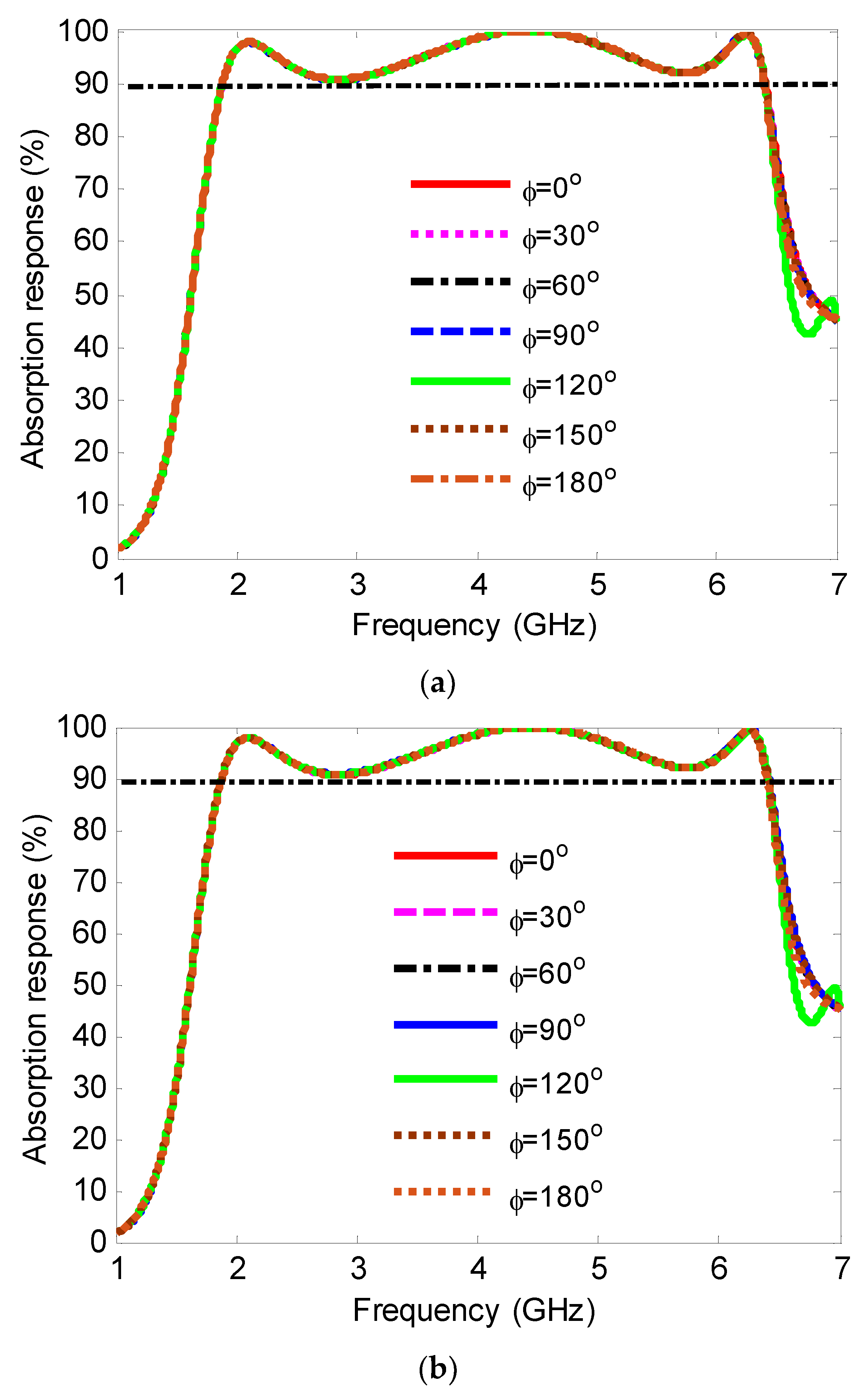
3.2. Absorption Mechanism at Different Polarization and Incident Angles

In practice, the direction of the EM wave is unknown. So that the design of the MS absorber capable of collecting ambient EM energy with characteristics of polarization insensitivity and a wide incident angle from 0 ° up to 60 ° is desirable. Numerical simulation was conducted to investigate the MS absorber’s polarization and oblique incident angle properties. Figure 7a,b show the simulated absorption of the MS absorber when the polarization angle ( ϕ ) changes from 0 ° up to 180 ° in the step of 30 ° for TE- and TM-polarization. The MS structure’s symmetrical design results in similar absorption responses for the TE- and TM-polarizations. As shown in Figure 7, the proposed MS absorber provides stable performance, confirming that it could deal with the vertical, horizontal, and circular polarization signals.
Figure 8a,b shows the simulated absorption responses for TE-polarized and TM-polarized incident angles, respectively. For TE-polarized incident angles, an absorption ratio of about 80% is achieved with various incident angles up to 45 ° at a wider frequency range, as shown in Figure 8a. At angle of 60 ° , the absorption ratio drops below 80% for the frequency band from 2.19 GHz to 3.9 GHz. For TM-polarized incident angles, the absorption ratio remains steady up to 30 ° , as shown in Figure 8b. When the incident angle increases above of 30 ° , the absorption ratio of about 80% is achieved. At the frequency band from 4.43 GHz up to 4.7 GHz, the absorption ratio drops to 65%. Based on the above explanation, the absorption responses decreased with increasing incidence angles and decreasing incident magnetic flux between the top and bottom layers.

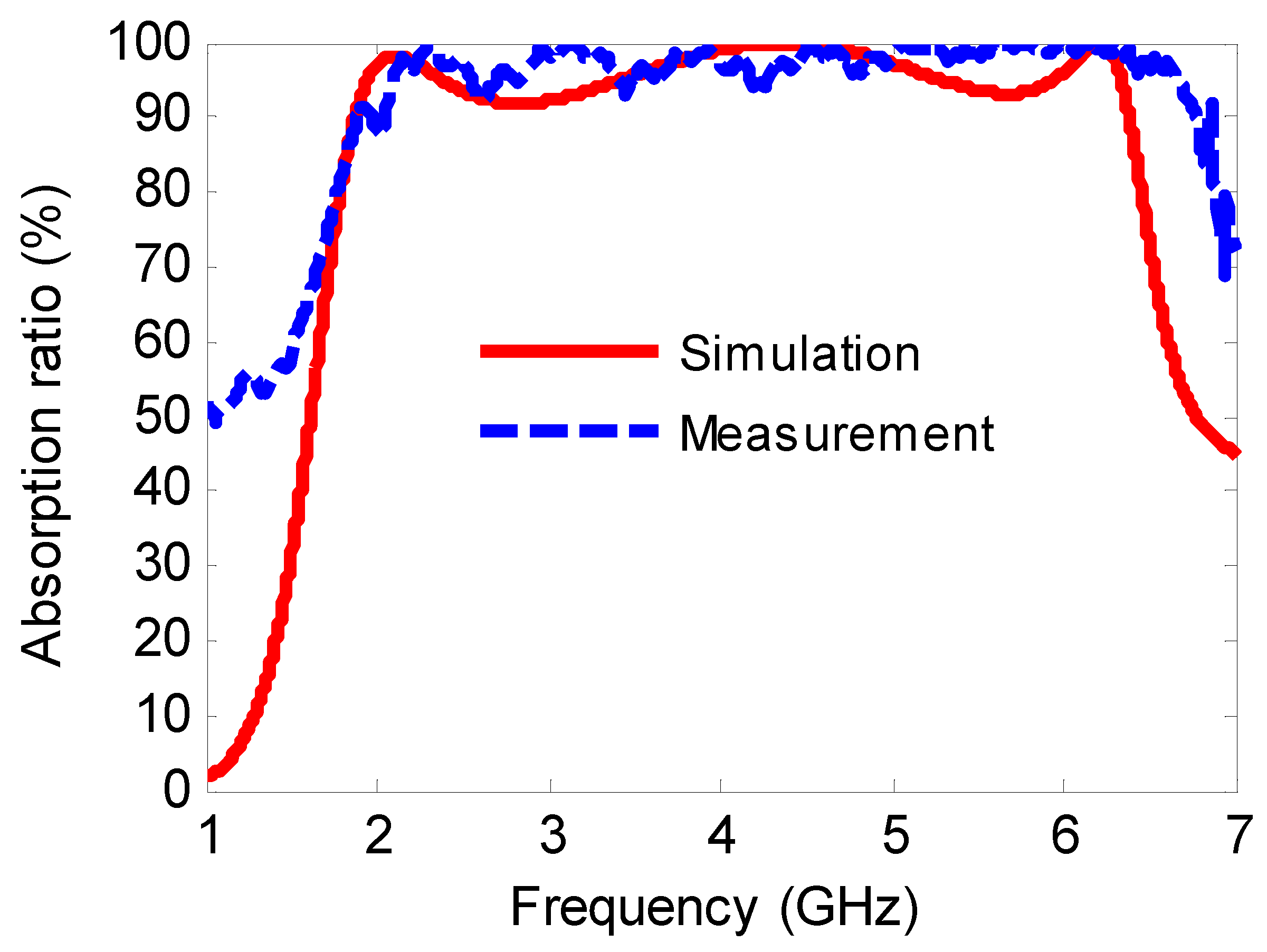
4. Measurement Verification

Measurement verification of the MS absorber was achieved by prototyping a structure of 7 × 7 unit cells with an overall dimension of 280   mm × 280   mm . Figure 9 shows the MS prototyped structure using PCB technology and measurement setup. The MS resonator is printed on the top of the FR4 layer, where each resonator is connected with four resistor loads to achieve broadband, as shown in Figure 9a. The full copper plate is covered the top view of the bottom FR4 to serve as a ground plane. The top and bottom FR4 substrates are physically connected and supported using four dielectric plastic screws. Full-wave simulation using CST MWS demonstrates that the plastic screws do not affect on the reflection coefficient. The measurement was conducted using two horn antennas (type HF906) as transmitter and receiver, which are then connected to the E5071C vector network analyzer (VNA) ports, as shown in Figure 9b. Tapered wedge absorbers surround the test MS absorber sample to remove the unwanted reflection from the surrounding area/environment. The horn antenna was placed 1 m away from the MS absorber to achieve the maximum radiation power [29]. The measured absorptivity of the proposed absorber was calculated from the reflection coefficient. To begin, reference measurements are taken on a metal surface of the size of the proposed absorber to normalize the measurement results. Then, the fabricated sample is positioned, and the reflection coefficient is measured. The difference between reflected powers from the metal and the fabricated sample is the actual reflection coefficient of the proposed MS absorber. The simulated and measured absorptivity of the fabricated MS absorber sample is shown in Figure 10. It is clear that the measured absorptivity agrees reasonably well with the simulation result except for the small discrepancy caused by the tolerance of the fabrication, especially the height of the air layer and measurement setup. The measured absorptivity above 90% is achieved at the frequency range from 1.89 GHz to 6.85 GHz, and the relative bandwidth is about 113.5%.
The proposed MS absorber is compared with previously published MMAs in terms of the total thickness, fractional bandwidth, maximum polarization, incident angles, and resistor loads. The proposed MS absorber, as shown in Table 1, has a fractional bandwidth of 113% and provides a higher absorbance for various polarization and incident angles. Furthermore, the proposed MS absorber has fewer resistor loads and a simple structure with easy fabrication.

5. Conclusions

A broadband MS absorber in the lower frequency range has been demonstrated experimentally for RF energy harvesting and wireless power transfer applications. It was designed based on the square resonator with four splits loaded with lumped resistors to absorb a wide frequency range efficiently. The proposed MS absorber is polarization-insensitivity and shows a broadband absorption for an oblique incidence angle up to 60 ° for both TE and TM polarizations. Further simulations reveal that the MS structure and lumped resistors have the optimized geometric parameters for achieving the highest absorption coefficient and the widest bandwidth. To better understand the absorption mechanism, E-field and surface current distributions have been presented. Finally, the proposed MS absorber was fabricated and tested to verify the simulated results. Experimental results show that the proposed MS absorber achieves an absorption spectrum of more than 90% in the frequency band from 1.89 GHz up to 6.85 GHz, with the widest fractional bandwidth of up to 113%. Such a broadband MS absorber may be used in different applications such as 5G new radio (5G NR)/EM harvesting, stealth technology, etc.

Author Contributions

Conceptualization, A.A.G.A. and S.Z.S.; methodology, A.A.G.A., S.Z.S., N.N., A.A., A.A.S. and S.S.M.G.; software, A.A.G.A. and S.Z.S.; validation, A.A.G.A., S.Z.S., N.N. and A.A.; formal analysis, A.A.G.A., S.Z.S. and S.S.M.G.; investigation, A.A.G.A., S.Z.S. and N.N.; resources, A.A.G.A. and S.S.M.G.; data curation, A.A.G.A., S.Z.S. and N.N.; writing—original draft preparation, A.A.G.A.; writing—review and editing, A.A.G.A., S.Z.S., A.A., N.N. and S.S.M.G.; visualization, A.A.G.A., S.Z.S. and N.N.; supervision, S.Z.S.; project administration, S.Z.S., N.N. and A.A.S.; funding acquisition, A.A.G.A. and S.Z.S. All authors have read and agreed to the published version of the manuscript.

Funding

This work is supported by Taif university Researchers Supporting Project TURSP-2020/34, Taif University, Taif, Saudi Arabia and Universiti Tun Hussein Onn Malaysia Publisher’s Office via Publication Fund E15216.

Acknowledgments

The authors thank Taif University Researchers Supporting Project TURSP-2020/34, Taif University, Taif, Saudi Arabia for supporting this work. Furthermore, Communication of this research is made possible through monetary assistance by Universiti Tun Hussein Onn Malaysia and the UTHM Publisher’s Office via Publication Fund E15216 and Universiti Teknologi Malaysia (UTM) for the Post-Doctoral Fellowship Scheme under the Professional Development Research University Grant (05E68).

Conflicts of Interest

The authors declare no conflict of interest.

References

  1. Shukoor, M.A.; Dey, S.; Koul, S.K. A Simple Polarization-Insensitive and Wide Angular Stable Circular Ring Based Undeca-Band Absorber for EMI/EMC Applications. IEEE Trans. Electromagn. Compat. 2021, 63, 1025–1034. [Google Scholar] [CrossRef]
  2. Munaga, P.; Ghosh, S.; Bhattacharyya, S.; Chaurasiya, D.; Srivastava, K.V. An Ultra-thin Dual-Band Polarization-Independent Metamaterial Absorber for EMI/EMC Applications. In Proceedings of the 2015 9th European Conference on Antennas and Propagation (EuCAP), Lisbon, Portugal, 13–17 April 2015; Volume 2, pp. 11–14. [Google Scholar]
  3. Chung, B.K.; Chuah, H.T. Modeling of RF absorber for application in the design of anechoic chamber. Prog. Electromagn. Res. 2003, 43, 273–285. [Google Scholar] [CrossRef] [Green Version]
  4. Kazemzadeh, A.; Karlsson, A. Multilayered wideband absorbers for oblique angle of incidence. IEEE Trans. Antennas Propag. 2010, 58, 3637–3646. [Google Scholar] [CrossRef] [Green Version]
  5. Bucci, O.M.; Franceschetti, G. Scattering from Wedge-Tapered Absorbers. IEEE Trans. Antennas Propag. 1971, 19, 96–104. [Google Scholar] [CrossRef]
  6. Ha, J.; Shin, W.; Lee, J.H.; Kim, Y.; Kim, D.; Lee, Y.; Yook, J.G. Effect of plasma area on frequency of monostatic radar cross section reduction. J. Electromagn. Eng. Sci. 2017, 17, 153–158. [Google Scholar] [CrossRef] [Green Version]
  7. Min Zhong, M.Z. Influence of dielectric layer on negative refractive index and transmission of metal-dielectric-metal sandwiched metamaterials. Chin. Opt. Lett. 2014, 12, 041601–041603. [Google Scholar] [CrossRef] [Green Version]
  8. Landy, N.I.; Sajuyigbe, S.; Mock, J.J.; Smith, D.R.; Padilla, W.J. Perfect metamaterial absorber. Phys. Rev. Lett. 2008, 100, 207402. [Google Scholar] [CrossRef]
  9. Faruque, M.R.I.; Rahman, M.; Hasan, M.M.; Famim, A.M.; Idrus, I.N.; Islam, M.T. Architecture of left-handed metamaterial absorber for absorbing electromagnetic hazards. J. Optoelectron. Adv. Mater. 2020, 22, 495–500. [Google Scholar]
  10. Amer, A.A.G.; Sapuan, S.Z.; Nasimuddin, N.; Alphones, A.; Zinal, N.B. A comprehensive review of metasurface structures suitable for RF energy harvesting. IEEE Access 2020, 8, 76433–76452. [Google Scholar] [CrossRef]
  11. Amer, A.A.G.; Sapuan, S.Z. Nasimuddin Multi-Band Metasurface Microwave Absorber Based on Square Split-Ring Resonator Structure. In Proceedings of the 12th National Technical Seminar on Unmanned System Technology 2020; Lecture Notes in Electrical Engineering; Springer: Singapore, 2022; Volume 770, pp. 373–382. [Google Scholar] [CrossRef]
  12. Amer, A.A.G.; Sapuan, S.Z.; Nasimuddin, N.; Hassan, M.F. A Broadband Wide-Angle Metasurface Absorber for Energy Harvesting Applications. In Proceedings of the 2021 International Conference of Technology, Science and Administration (ICTSA), Taiz, Yemen, 22–24 March 2021. [Google Scholar] [CrossRef]
  13. Bakır, M.; Karaaslan, M.; Unal, E.; Akgol, O.; Sabah, C. Microwave metamaterial absorber for sensing applications. Opto-Electron. Rev. 2017, 25, 318–325. [Google Scholar] [CrossRef]
  14. Hajizadegan, M.; Ahmadi, V.; Sakhdari, M. Design and analysis of ultrafast and tunable all optical metamaterial switch enhanced by metal nanocomposite. J. Light. Technol. 2013, 31, 1877–1883. [Google Scholar] [CrossRef]
  15. Xiong, H.; Hong, J.S.; Luo, C.M.; Zhong, L.L. An ultrathin and broadband metamaterial absorber using multi-layer structures. J. Appl. Phys. 2013, 114, 064109. [Google Scholar] [CrossRef]
  16. Soheilifar, M.R.; Sadeghzadeh, R.A. Design, fabrication and characterization of stacked layers planar broadband metamaterial absorber at microwave frequency. AEU-Int. J. Electron. Commun. 2015, 69, 126–132. [Google Scholar] [CrossRef]
  17. Tang, J.; Xiao, Z.; Xu, K.; Ma, X.; Wang, Z. Polarization-Controlled Metamaterial Absorber with Extremely Bandwidth and Wide Incidence Angle. Plasmonics 2016, 11, 1393–1399. [Google Scholar] [CrossRef]
  18. Sheokand, H.; Ghosh, S.; Singh, G.; Saikia, M.; Srivastava, K.V.; Ramkumar, J.; Ramakrishna, S.A. Transparent broadband metamaterial absorber based on resistive films. J. Appl. Phys. 2017, 122, 105105. [Google Scholar] [CrossRef]
  19. Cheng, Y.Z.; Wang, Y.; Nie, Y.; Gong, R.Z.; Xiong, X.; Wang, X. Design, fabrication and measurement of a broadband polarization-insensitive metamaterial absorber based on lumped elements. J. Appl. Phys. 2012, 111, 2010–2014. [Google Scholar] [CrossRef]
  20. Yuan, W.; Cheng, Y. Low-frequency and broadband metamaterial absorber based on lumped elements: Design, characterization and experiment. Appl. Phys. A Mater. Sci. Process. 2014, 117, 1915–1921. [Google Scholar] [CrossRef]
  21. Lim, D.; Lim, S. Ultrawideband Electromagnetic Absorber Using Sandwiched Broadband Metasurfaces. IEEE Antennas Wirel. Propag. Lett. 2019, 18, 1887–1891. [Google Scholar] [CrossRef]
  22. Bağmancı, M.; Akgöl, O.; Özaktürk, M.; Karaaslan, M.; Ünal, E.; Bakır, M. Polarization independent broadband metamaterial absorber for microwave applications. Int. J. RF Microw. Comput. Eng. 2019, 29, e21630. [Google Scholar] [CrossRef] [Green Version]
  23. Chen, K.; Luo, X.; Ding, G.; Zhao, J.; Feng, Y.; Jiang, T. Broadband microwave metamaterial absorber with lumped resistor loading. EPJ Appl. Metamater. 2019, 6, 1. [Google Scholar] [CrossRef] [Green Version]
  24. Zhao, J.; Cheng, Y. Ultrabroadband Microwave Metamaterial Absorber Based on Electric SRR Loaded with Lumped Resistors. J. Electron. Mater. 2016, 45, 5033–5039. [Google Scholar] [CrossRef]
  25. Banadaki, M.D.; Heidari, A.A.; Nakhkash, M. A Metamaterial Absorber with a New Compact Unit Cell. IEEE Antennas Wirel. Propag. Lett. 2018, 17, 205–208. [Google Scholar] [CrossRef]
  26. Wang, Q.; Cheng, Y. Compact and low-frequency broadband microwave metamaterial absorber based on meander wire structure loaded resistors. AEU-Int. J. Electron. Commun. 2020, 120, 153198. [Google Scholar] [CrossRef]
  27. Bakir, M.; Karaaslan, M.; Dincer, F.; Delihacioglu, K.; Sabah, C. Perfect metamaterial absorber-based energy harvesting and sensor applications in the industrial, scientific, and medical band. Opt. Eng. 2015, 54, 097102. [Google Scholar] [CrossRef]
  28. Amer, A.A.G.; Sapuan, S.Z.; Nasimuddin, N. Efficient Metasurface Absorber for 2.4 GHz ISM-Band Applications. In Proceedings of the 2020 IEEE Student Conference on Research and Development (SCOReD), Batu Pahat, Malaysia, 27–29 September 2020; pp. 471–474. [Google Scholar] [CrossRef]
  29. Amiri, M.; Tofigh, F.; Shariati, N.; Lipman, J.; Abolhasan, M. Miniature tri-wideband Sierpinski-Minkowski fractals metamaterial perfect absorber. IET Microw. Antennas Propag. 2019, 13, 991–996. [Google Scholar] [CrossRef]
  30. Kalraiya, S.; Chaudhary, R.K.; Abdalla, M.A. Design and analysis of polarization independent conformal wideband metamaterial absorber using resistor loaded sector shaped resonators. J. Appl. Phys. 2019, 125, 134904. [Google Scholar] [CrossRef]
  31. Kalraiya, S.; Chaudhary, R.K.; Abdalla, M.A. Resistor loaded wideband conformal metamaterial absorber for curved surfaces application. AEU-Int. J. Electron. Commun. 2022, 143, 154033. [Google Scholar] [CrossRef]
  32. Jang, T.; Youn, H.; Shin, Y.J.; Guo, L.J. Transparent and Flexible Polarization-Independent Microwave Broadband Absorber. ACS Photonics 2014, 1, 279–284. [Google Scholar] [CrossRef]
  33. Kong, X.; Xu, J.; Mo, J.J.; Liu, S. Broadband and conformal metamaterial absorber. Front. Optoelectron. 2017, 10, 124–131. [Google Scholar] [CrossRef]
  34. Smith, D.R.; Vier, D.C.; Koschny, T.; Soukoulis, C.M. Electromagnetic parameter retrieval from inhomogeneous metamaterials. Phys. Rev. E-Stat. Nonlinear Soft Matter Phys. 2005, 71, 036617. [Google Scholar] [CrossRef] [Green Version]
  35. Zuo, W.; Yang, Y.; He, X.; Zhan, D.; Zhang, Q. A miniaturized metamaterial absorber for ultrahigh-frequency RFID system. IEEE Antennas Wirel. Propag. Lett. 2017, 16, 329–332. [Google Scholar] [CrossRef]
  36. Zuo, W.; Yang, Y.; He, X.; Mao, C.; Liu, T. An ultrawideband miniaturized metamaterial absorber in the ultrahigh-frequency range. IEEE Antennas Wirel. Propag. Lett. 2017, 16, 928–931. [Google Scholar] [CrossRef]
Figure 1. Geometry of proposed MS absorber: (a) perspective view, (b) side view, and (c) top view.
Electronics 11 01986 g001
Figure 2. Boundary setup in CST.
Electronics 11 01986 g002
Figure 3. Simulated absorption coefficients: (a) simulated absorption and reflection under normal incidence, (b) absorption under two different loss conditions, and (c) the absorption of the MS absorber with and without resistor loads.
Electronics 11 01986 g003
Figure 4. E-field distributions: (a) 2.09 GHz, (b) 4.34 GHz, and (c) 6.2 GHz.
Electronics 11 01986 g004
Figure 5. Surface current distributions: (a) 2.09 GHz, (b) 4.34 GHz, and (c) 6.2 GHz.
Electronics 11 01986 g005
Figure 6. Simulated absorption spectra of the MS absorber: (a) air layer thickness, (b) outer resonator’s width, (c) inner resonator’s width, (d) split’s size, and (e) load resistor.
Electronics 11 01986 g006
Figure 7. Simulated absorption ratio for various polarization angles: (a) TE-polarized and (b) TM-polarized.
Electronics 11 01986 g007
Figure 8. Simulated absorption ratio for various incident angles: (a) TE-polarized and (b) TM-polarized.
Electronics 11 01986 g008
Figure 9. (a) Fabricated prototyped of MS absorber and (b) measurement setup.
Electronics 11 01986 g009
Figure 10. Measured and simulated absorption coefficient.
Electronics 11 01986 g010
Table 1. Comparison with other wideband MS absorbers having air layer and loaded with lumped resistors.
Refs. F L   ( GHz ) Total
Thickness
Fractional BW (%)Max Polarized AngleMax Incident AngleResistor
No
[25]1.35 ( 0.097   λ L ) 8845608
[26]1.84 ( 0.071   λ L ) 105.675504
[30]3.9 ( 0.098   λ L ) 91.690604
[35]0.86 ( 0.062   λ L ) 16.430304
[36]0.8 ( 0.071   λ L ) 108.530308
This work1.88 ( 0.097   λ L ) 113180604
Publisher’s Note: MDPI stays neutral with regard to jurisdictional claims in published maps and institutional affiliations.

