Abstract
Considering the disadvantages of the traditional development pattern in an embedded control system for an inverter, that is, the single-process thinking and separation of software and hardware, a novel method, which is a model-based design, for developing a double closed-loop control system for the diode-clamped three-level inverter was proposed. System control models, including the PWM control algorithm model, the voltage control model, the neutral-point potential balancing model, and the frequency control model, were built with the MATLAB platform. The code-generation capacity and the operation effect were verified through a series of tests. The inverter with diode clamp and neutral-point potential control was developed. Codes were generated automatically and downloaded to the eZdsp28335 control chip. Experimental waveforms of the phase voltage, line voltage and current were analyzed under regulating the voltage and frequency. The experimental results demonstrate that the models and the generated codes are correct. Further studies have proven the feasibility of the system development model.
1. Introduction
The three-level inverter has advantages, such as having a value close to the sine wave output voltage that can reduce the withstanding voltage rating and switching loss of the device, etc. [1,2,3]. The three-level inverter has been widely used in power, metallurgy, mining, petrochemical, and other occasions [4,5,6,7]. The control module is the main part to realize the three-level inverter. The scholars [2,5,6] adopted DSP as a controller. In [7], the researchers combined DSP and FPGA to achieve the complexed control. The traditional software development process of the control system for the three-level inverter includes four stages. They are: software requirements analysis, design model, code realization, and a system test [8,9]. The completion of each phase is usually achieved by different engineers, in which the design documents that form this stage are isolated from each other. An error of understanding often occurs because of document communication, which results in many hidden dangers to the whole design [10,11]. After the completion of the whole design project, manual programming is used to check the error in the entire development cycle. It leads to low efficiency and low precision, resulting in repeated labor and prolonged labor time, which makes the test difficult [12].
The model-based design technology, which gradually improved after a decade of development, has been widely accepted. Based on the Embedded Coder toolbox developed by TI and Math Works Company, the model-based design introduces a new approach for control system development, such as in the robotic system, automotive, aerospace, and other fields [13,14,15,16,17]. This approach has adopted the model-based design method. In recent years, the model-based design method has been often used in the development of hybrid electric vehicle control systems. Its advantage lies in the organic integration of the four stages of the traditional development process [18,19]. Validation and testing begins from the demand analysis stage on the MATLAB platform. Engineers focus their energy on the study of algorithms and test cases. The embedded C code programming leads to complete automation, thereby effectively reducing the possibility of human error. This program not only improves the reliability and consistency of the code but also speeds up the development of software and hardware. Meanwhile, it can shorten the development cycle and improve the quality of the product [20,21,22,23].
In this study, the method of model-based design is introduced into the design of a frequency-voltage double closed-loop control system for the three-level inverter. A novel development method of control system is proposed. Based on analysis of the MATLAB environment to achieve the model-based design method, the overall design process of the entire system is established. The pulse-width modulation (PWM) control algorithm, voltage control, frequency control, and neutral-point potential-balancing control models are developed. The entire design process is integrated to complete the verification and optimization of the model and to automatically generate codes.
The rest of the paper is organized as follows: Section 2 describes the proposed framework, including the control method and the underlying models. The model verification cation and the generation of control code are presented in Section 3. Section 4 presents an experimental validation and results. Section 5 and Section 6 propose, respectively, the discussion and conclusions of this study.
2. Proposed Model-Based Design Framework for Inverter System
MATLAB/Simulink is treated as the developed platform implementing the model-based design in consideration of cost and application [24]. The overall framework of the frequency-voltage double closed-loop inverter system based on model design is proposed, as illustrated in Figure 1.
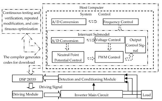
Figure 1.
Model-based control design framework.
The control system based on the method of model design is carried out in the upper part of the computer. A model is established after constant testing and verification, and it is then converted into an automatically generated code. After that, the code is downloaded to the main control chip digital signal processor (DSP) to control the hardware circuit inverter.
The main circuit of the inverter adopts the three-phase, three-level topology with diode clamp, as shown in Figure 2.
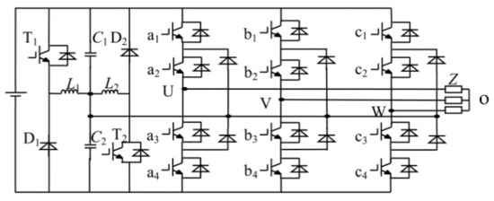
Figure 2.
Main circuit of a diode-clamped three-level inverter.
For the three-phase output voltage, the phase voltage can be expressed by SU, SV, and SW and the DC side power supply as Udc. They are
The three-phase line voltage of the output voltage can be expressed as
The imbalance of the neutral-point potential will lead to an increase in the low harmonic content of output voltage and waveform distortion. Therefore, a neutral-point potential-balancing structure is added in the hardware control. Compared with the software control method, the original control method does not need to be modified in the proposed method. The influence of the rear main circuit is also disregarded. The system can control the balance of the neutral-point potential regardless of whether or not it works in active or reactive power or large modulation [25].
In Figure 2, L1 and L2 are the energy-storage inductors, and D1 and D2 are the fly-wheel diodes. Based on the neutral-point value, the on–off of the power switches T1 and T2 is controlled immediately. The loading voltage of voltage balance capacitors C1 and C2 is controlled and the balance of neutral-point potential is achieved accordingly.
2.1. Model of PWM Control
Considering the shortening of the development cycle and the optimization of the model, the triangular carrier reverse-phase stack PWM is determined to be the control strategy [26]. Taking U-phase as an example, the principle of reverse stack PWM control method is shown in Figure 3.
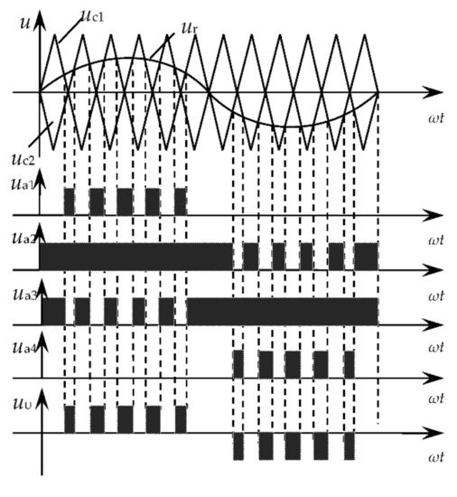
Figure 3.
Principle diagram of carrier inverse disposition.
The upper carrier wave uc1 and the lower carrier wave uc2 with an opposite phase to uc1 are compared with the same modulation wave ur. Taking one phase as an example, the control waves of switches al and a3 are opposing and signals of a2 and a4 are opposing. The PWM resulting from modulation wave ur in comparison with the upper carrier uc1 are thus used to control the on–off of al and a3. The PWM resulting from modulation wave ur in comparison with the lower carrier uc2 are used to control the on–off of a2 and a4.
The sine wave modulation function is us = Ussinωt, Mu = Us/Uc (Mu is the modulation index, 0 ≤ Mu ≤ 1; Uc is the amplitude of carrier wave). Further analysis is carried out by using the symmetrical regular sampling method. The mathematical principle of the PWM control method of the carrier reverse-phase stack PWM can be acquired.
where ton is the time of high-level output and T is the cycle of triangle carrier wave. The duty ratio of each cycle can be calculated using this formula. The sampling time is t, which is determined by the carrier ratio N, ωt = k*2π/N, k = 0, 1, 2, 3 … N − 1. The value of the sine function at the sampling time generated from the lookup table can indicate the duty ratio of PWM control wave on each triangular carrier cycle. x1–x4 (where x = a, b, c) are the four power switches of each phase bridge arm. x1 and x4 can be obtained following mathematical principles; x2 and x3 are the reverse of x1 and x4. x1 can be determined through the upper carrier wave in comparison with modulation wave. x4 can be identified through the lower carrier in comparison with modulation wave.
The sine wave is divided into equal intervals based on the carrier ratio. The corresponding sine value of each point is the required value of sinωt. The duty ratio of PWM in each carrier cycle can be determined according to Mu and sinωt. The value of Mu is set to 0.8. The carrier ratio is set to 12. According to the principle of periodic repetition of the sine wave, a three-phase modulation wave covered by twelve carrier cycles is a complete three-phase alternating current cycle. Taking a1 as an example, the control model of PWM is shown in Figure 4.
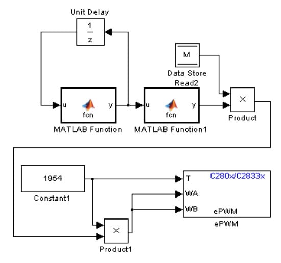
Figure 4.
PWM control model.
2.2. Model of Voltage Control
Voltage regulation can be realized by controlling the modulation index Mu. The control model of the system voltage is shown in Figure 5.
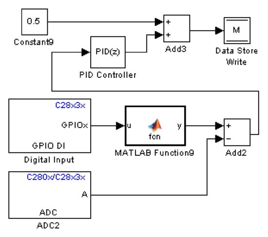
Figure 5.
Voltage control model.
Digital input module is added to the model to invoke the input/output (I/O) port of DSP. The given voltage value of the system is changed following the high–low potential of the input of the I/O port. The MATLAB Function9 is loaded with the given values corresponding to different input values of the I/O port. The DSP28335 analog-to-digital converter (ADC) module is added to return the actual voltage of the inverter system to the DSP. The deviation of the actual value and the given value is sent to the proportional–integral–derivative regulator. The value of Mu is adjusted to reduce the deviation between the given and actual value. The initial value of Mu is set to 0.5 to guarantee the response speed of the system.
2.3. Model of Neutral-Point Potential Control
Although the diode-clamped, three-level topology has the advantage of simple structure, it also has the disadvantage of neutral-point potential unbalance. The deviation of the neutral-point potential is caused by the parameters of the power switch and the size of the grading capacitor. Moreover, the working condition of the system and the control method can lead to fluctuation of the neutral-point potential. Furthermore, a significant active component of the inverter output leads to high magnitude of the tilt, reactive component of the output, and amplitude of fluctuation [27]. Hence, controlling neutral-point potential is necessary. Based on the control method of neutral-point potential, T1 and T2 switches are also controlled by building model and generating code with DSP. The model of neutral-point potential control is shown in Figure 6.
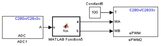
Figure 6.
Control model of neutral-point potential.
The neutral-point potential in the circuit is returned to the analog-to-digital (A/D) interface of the DSP after sampling. The DSP28335 ADC module is added to the model, and the port and the working method are selected. The results of A/D conversion are evaluated through the MATLAB Function5. A is the output port and B is not the output port when the result is higher than the given value. The opposite occurs when the result is lower than the given value. The corresponding cycle count is set in the ePWM2 module. When neutral-point potential drifts, A and B ports can output PWM waves with a certain duty ratio to control the on–off of the two switches to control the neutral-point potential.
2.4. Model of Frequency Control
The output frequency of inverter can be adjusted by changing the frequency of PWM wave. Figure 7 shows the control model of the inverter.
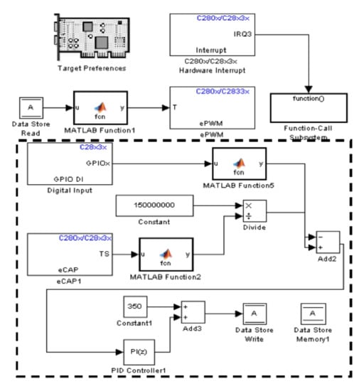
Figure 7.
Model of the inverter control.
The DSP28335 function module and interrupt program module are added to the model. Regarding ePWM module as an interrupt source, the duty ratio of the next cycle is calculated in every interrupt subprogram. The models of voltage control, neutral-point voltage control, and control algorithm are integrated into the interrupted sub model to control the closed loop of voltage loop. Frequency control and interrupt program models are also integrated into the main model to control the closed loop of frequency loop. By combining the two parts, the double closed-loop control structure of frequency and voltage can be obtained.
Given that the frequency of the PWM control algorithm is determined by the interrupt time and the cycle time, the two parameters should be synchronously changed in the model. The dashed frame shown in Figure 7 is the frequency control model. The DSP28335 eCAP module is added to the model to capture and adjust the square wave signal that comes from the output current signal of the system. Capture port and capture method are selected. Two rising edges are then captured continuously. MATLAB Function2, which is behind the DSP28335 eCAP module, counts by subtracting to calculate the output frequency of the system. The given frequency of the I/O port is introduced into the system using the input digital module. The deviation of given frequency and output frequency is sent to the proportional–integral (PI) regulator to change the interrupt time and the control cycle of PWM.
3. Reliability Assurance and Control Implementation
The functional verification, model advisor, software-in-the-loop (SIL) test, and processor-in-the-loop (PIL) test are necessary to ensure the correctness of the model and the reliability of the results. The established carrier stack PWM model is adopted and is extended into three phases. The control signal of the model output is connected with the simulation model of the inverter system to perform functional verification.
3.1. Verification and Validation of Models
Functional verification is similar to the traditional simulation. In the traditional simulation of a power electronic system, virtual hardware is used to set up the system and the system principle is further understood or the circuits are verified. The model-based design has a stronger boundary to control parts and controlled parts. The most important effect of functional verification is to verify the function correctness of control parts and whether they can control the controlled object to achieve the ideal effects as expected or not.
In this study, a three-phase three-level inverter is built under MATLAB/Simulink. Its control part adopts the mathematic model established in the previous section and is extended for the three-phase control. Control signals outputted from the mathematic model are connected to the inverter in order to validate the output results of the inverter. The duty ratio and cycle are needed in the processor so that PWM pulses are created by comparing the triangular wave with the duty-ratio signal. One computational model corresponds with the control of one switch. Six computational models are for control signals of a1, a4, b1, b4, c1, c4 in Figure 2, respectively. Control signals of a2, a3, b2, b3, c2, c3 in Figure 2 are obtained by inverting those signals.
Figure 8 presents the output wave-form of UV line voltage after the functional verification. It shows that the line voltages are in five levels. Currents vary as the sine wave under the resistor–inductor load. The feasibility of building a control model from the mathematical model and the correctness of the control algorithm model are proven.
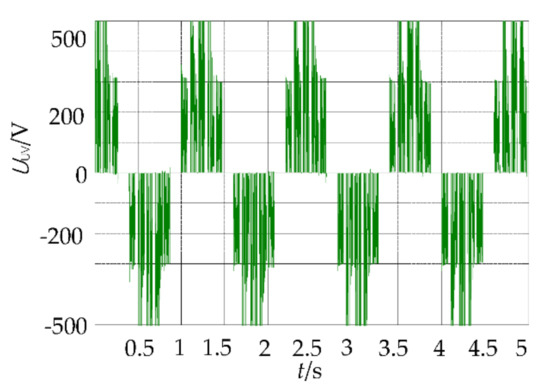
Figure 8.
Line voltage waveform of functional verification.
The model advisor in MATLAB can identify the defective parts and the parts limiting the model’s efficiency. These parts usually cannot generate codes or generate invalid codes, present the examination results of the model, and give suggestions on how to modify the model. A Simulink and Embedded Coder, which determine the code quality, are selected to check the model.
The SIL test is conducted to evaluate the embedded code generated by the model, to complete the early validation of the code, and to replace the test results of rapid prototyping. Taking two algorithm models of U-phase as example, the SIL module is converted after modifying the output module. When the SIL module is generated, MATLAB provides the code report that contains all code files. The results are consistent with the output of the original model after running the SIL module. The SIL module can thus realize the function of the original model. The package codes can describe the model function to be realized completely. The SIL test results show the correctness of the model-generated codes.
This study also tests the PIL to verify and optimize the algorithm model. The PIL downloads the C codes that are automatically generated in the control model into the processor, and these C codes perform a non-real-time simulation with the control model. The running status of the code on the processor is evaluated, and results show the error caused by the target compiler or processor and the lack of the capability of bearing codes of the processor. All the algorithms that the system needs are included into the control model. The PIL module is generated and tested by configuring the model. When the PIL module is operated, eZdsp28335 works in debug state, and Code Composer Studio (CCS) starts its operation automatically. The data from the processor output are exchanged with the controlled object model data from the MATLAB through a USB cable. The PIL module output indicates that the code operation meets the requirements, and this indirectly proves the reliability of the control algorithm model.
After verifying the model through an off-line stimulation, this study also validates the coverage rate of the model, the underlying driver of the generated code, and the integrity of the data stream. Finally, an accurate and reliable model is acquired to generate codes.
3.2. Automatic Generation of Code
The main idea of this design is based on using the timing interrupt of DSP. The duty ratio of the next cycle is calculated in each interrupt subprogram. Therefore, PWM control waveforms with constant changes are seen. The time of timing interruption decides the frequency of PWM waveform and the output frequency of inverter. Consequently, the module of interruption program should be added to the model. Figure 9 illustrates the code-generation model after adding the DSP28335 functional modules.
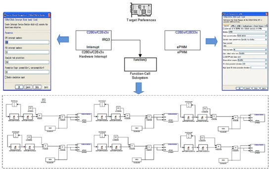
Figure 9.
Code-generation models.
Module ePWM is used as the interrupt source, and we enable ePWM3 by setting which cycle is the time of timing interruption. The frequency of DSP is 150 MHz. When the desired frequency of AC outputs is 50 Hz, the carrier ratio is set as 12 and 128 prescales are set to the TB clock. According to the operation, it can be seen that 150 M/128/50/12 = 1954. It should be filled in the module ePWM by double-clicking it, and ePWM cycle interruption is started in the window of Event Trigger. Thus, the setting of ePWM is completed. The interrupt vector corresponding with ePWM3 is 3-3 in view of the interrupt vector table of DSP28335. By double- clicking the module of Hardware Interrupt, the interrupt number of CPU is set to 3 and the interrupt number of PIE is set to 3.
The six models of control to three phases are placed into the Function-Call Subsystem as the interrupt models and then transformed into codes that are the interrupt subprograms. For outputting PWM control signals, the module ePWM is added in the control module. The cycle T is similarly equivalent to the interrupt time, which is set to 1954 after 128 prescale, and times of high level and low level are obtained by multiplying the duty ratio. The times are sent to two ports of module ePWM that are set as the opposite. Then, a group of complementary PWM signals are gained and, in the window of Deadband Unit, the dead times of two-port signals should be set so as to protect switches.
After adding the DSP28335 functional module, the model has met the condition to generate codes used in DSP28335 directly. TMS320F28335 is set as the target chip by double-clicking the module Target Preferences. In the Configuration Parameters of the modeling window, the TLC file is selected and the target language are specified as C language. Connecting the development board of DSP 28335 with the computer, the compilation key is pressed and then the needed codes are generated. Meanwhile, MATLAB would provide the generated code report.
Before the code is generated, MATLAB checks the conformity between the computer processor and the model settings. The generated code contains all the header, library, and main files, which are needed to create the DSP projects. The model presenting the generated code corresponds to the codes, and this is helpful for the following amendments and upgrades. After the code is generated, MATLAB automatically connects to the target processor connected, creates a project file, and downloads the code to eZdsp28335 to operate. The entire process is completed automatically by the computer without manual operation. The process of codes from generation to operation is illustrated in Figure 10.
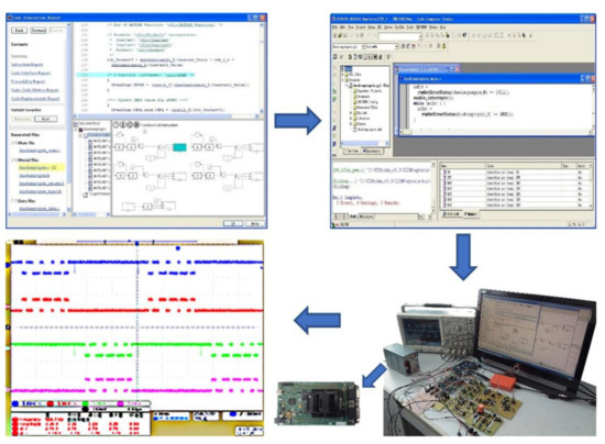
Figure 10.
Process of code generation.
It is observed on the oscillator shown in Figure 10 that PWM control signals of four switches, a1–a4, in the U-phase, which output from DSP, are coincident to the need in waveforms, and contain dead-band time so that the design requirements are fully met.
4. Experimental Validation
With the optimization of the system, the closed-loop control to the voltage, frequency, and neutral-point potential are realized. An experimental prototype of a diode-clamped three-phase, three-level inverter system is built to verify the control effect based on the model design.
The whole system consists of the computer, target controller, and hardware circuits. MATLAB runs in the computer and transforms models into the codes, which are compiled by CCS and downloaded to the target controller to control hardware circuits. Hardware circuits, illustrated in Figure 10, mainly include driving circuits, the main circuit of the inverter, and detection circuits of the voltage and frequency.
eZdsp28335 is selected as the control chip, IR2110 as the driving chip, and HOP voltage transformer and AD637 chip as the detection part. The validated and optimized model is compiled. Then, it automatically generates the code on the computer, downloads the code to eZdsp28335, and accesses the hardware circuit. The obtained control signal is driven by the driving circuit to control the insulated-gate bipolar transistor works in the main circuit. When the voltage regulation is controlled, the line voltage is used as the adjusting target. The I/O 6 port of the eZdsp28335 is the input of the given voltage and the I/O 7 port of the eZdsp28335 is the input of the given frequency value. When the input of the I/O port is changed from low level to high level, the frequency of the output line voltage and line current of the inverter system is accelerated. A gradual acceleration of the PI regulation process occurs, and the input of the I/O port changes from high level to low level, which is opposing. Therefore, frequency and voltage double closed-loop control can be realized.
Figure 11 shows the waveforms of the U-phase and V-phase voltage observed by the oscillator.
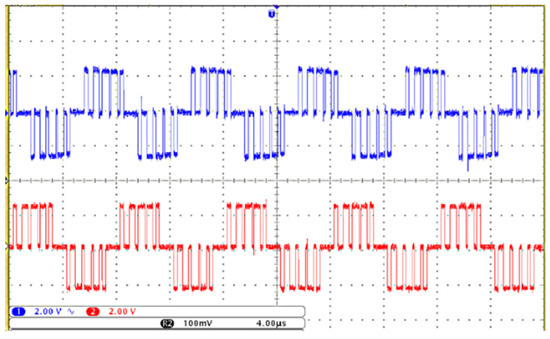
Figure 11.
Waveforms of phase voltage.
The phase voltage of each phase is a stable three-level voltage, and their phase difference is 120°.
The experimental waveforms of UV line voltage regulated from one value to another are made, as shown in Figure 12. The line voltage comprises five levels. The following current waveforms are given in Figure 13.
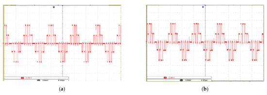
Figure 12.
Comparison waveforms of line voltage by regulating voltage: (a) before regulating, (b) after regulating.
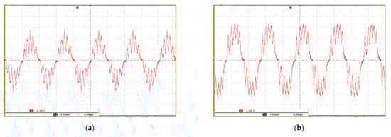
Figure 13.
Comparison waveforms of current by regulating voltage: (a) before regulating, (b) after regulating.
It is obviously observed that the pulse widths of inverter outputs broaden and the magnitudes of the currents become larger when the inputs of I/O change from low level to high level. In order to verify the system’s stability of regulating the voltage, the disturbance is set at the load side. The experiment is performed and shows that the voltage can be restored to the given value after the disturbance is added. This indicates that the function of regulating system voltage is perfect: on the one hand, the output voltage can be changed by altering the external input; on the other hand, the voltage can be stabilized when the disturbance exists. Thereby, the closed-loop control of the voltage is realized.
Since the frequency of the inverter can be needed to be adjustable in the test platform of docking mechanism, the experiments are conducted with regulating the frequency. As mentioned above, the output frequency of the inverter has a direct relationship with the frequency of PWM control wave. Therefore, the output frequency is changed by regulating the frequency of PWM wave. In the model, the frequency of the PWM control wave is determined by the time of timing interruption and the cycle time of PWM wave in the sub model. In this design, the two times are same; hence, they are altered synchronously in the model.
In the design, the current signals outputted from the inverter are processed into the square wave signal and sent back to the capture interface of DSP. The module DSP28335 eCAP is added in the model; the capture port and mode should be selected. When two rising-edge times are captured, MATLAB Function next to module eCAP subtracts count values of the two times. Then, the count value of the counter within one cycle is obtained. Thus, the output frequency of the inverter can be calculated.
Similarly, the module Digital Input is used as the rated frequency of I/O input system. The error of the rated frequency and output frequency is sent to PI regulator. The manipulated variable is achieved, by which the time of timing interruption and the cycle of PWM wave are changed. Port I/O 7 is used as the input. The low level denotes 50 Hz and the high level designates 80 Hz. When the frequency is changed, the waveforms of the line voltage and the current are measured on the oscillator seen in Figure 14 and Figure 15, respectively.
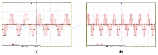
Figure 14.
Comparison waveforms of line voltage by regulating frequency: (a) before regulating, (b) after regulating.
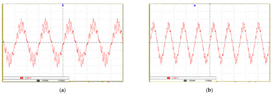
Figure 15.
Comparison waveforms of current by regulating frequency: (a) before regulating, (b) after regulating.
It is obviously seen that when the input of I/O port changes from the low level to the high level, the frequency of the line voltage and current quicken with the regulating process of PI quickly, step by step.
The output waveforms are transformed by FFT. The contents of the harmonic can be obtained under different control. The current harmonics are listed in Table 1. The effect of closed-loop control is better than that of open-loop control, and THD is reduced by 16.13%.

Table 1.
Comparisons of harmonic current under different control.
The waveform of the control effect of neutral-point potential is shown in Figure 16; Figure 16a,b are the neutral-point potential waveforms before and after the addition of neutral-point potential control. The comparison of the two waveforms shows that the addition of the neutral-point potential control model restrains the voltage deviation effectively. Additionally, as shown in Figure 16b, the PWM output waveforms of the switches T1 and T2 in the output neutral-point potential control circuit that is derived from the ePWMA and ePWMB of the ePWM2 port in Figure 6. The experimental results show that the code generated with the proposed method can realize the three-level control of inverter and the balance control of neutral-point potential.
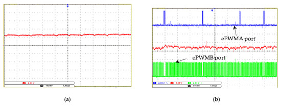
Figure 16.
Waveforms of neutral-point potential control: (a) before control, (b) after control.
5. Discussion
This paper researched the single-process thinking and the separation of hardware and software in the voltage-type inverter system, and investigated the solutions to its shortcomings. According to the investigation, multi-level instead of two-level can solve the problem of not being able to achieve high voltage and high power output, but it also creates the problem of control becoming relatively complex, despite these obvious advantages.
Firstly, the main design of the inverter system is planned, and the diode-clamped three-phase three-level inverter system is selected as the research objective. The main circuit is determined and its working principle is analyzed. Secondly, the carrier phase inversion cascade PWM control method is used as the control strategy. Considering that the control part is realized on the digital chip by the model-based design method, the mathematical model must be constructed by the model-based design method. The mathematical principle of the carrier phase inversion cascade PWM control method is analyzed and the neutral-point potential control method is determined. The mathematical model of the carrier phase inversion layer PWM control method is built, and a series of tests and verifications are carried out to ensure the integrity and correctness of the model. At the same time, the ability of the model to generate code and the ability of the target processor to carry out the code operation are tested, but the mathematical model of the controlled part is not constructed, so the whole design has room for improvement in reliability.
The control module is the key of the control system. Instead of programming, the specified control units in Ref. [7], OPAL-RT in Ref. [9], and Lab-VIEW NI in Ref. [10] are adopted to realize the control code. dSPACE and RT-LAB are often used in many fields, as well. However, the cost of these control units is very high. In this paper, a model-based design is presented to control the three-level inverter. The method is simple, economical, and convenient for the experiment in the laboratory.
The established mathematical model is used to develop the diode-clamped neutral- point potential control inverter, and the target processor is determined to be eZdsp28335. The function module of eZdsp28335 is added to the model, which constitutes the final code generation model. The code automatically generated by the model is downloaded to DSP, and the correctness of the design is verified by open-loop experiments. In order to improve the design, the model and hardware of frequency modulation, voltage regulation and neutral point potential control are added. Finally, a three-phase three-level inverter system with variable frequency and voltage regulation and neutral point potential control is completed. The code automatically generated by the model controls the operation of the whole system well. The author believes that this method has the advantages of high quality, high efficiency, and economy. This method can be extended to the development of embedded systems using in the power electronic system with more complex control methods and better system functions. However, there is no reliability verification in large-scale projects or high-risk projects. Subsequently, external hardware devices can be added to further verify the model design by rapid prototyping and hardware-in-the-loop methods.
6. Conclusions
A new approach with model-based design is presented in realizing a double closed-loop control for the three-level inverter. The PWM control, voltage control, neutral-point potential control, and frequency control are designed. A series of tests is conducted to verify the capability of the model for code generation and the operation effect. The three-level inverter system with frequency and voltage double closed-loop control is constructed, and the automatically generated C code is downloaded to the eZdsp28335 control chip. The experiments under open-loop and closed-loop control were performed and the waveforms were analyzed. The experimental results show the three-level control to the inverter is realized by the generated code, and the unbalance of neutral-point potential of diode-clamped three-level inverter is suppressed. Furthermore, the voltage and frequency can be adjusted with the change in load. This method significantly reduces the development costs and resource consumption. The feasibility and application value of the model-based design in the field of power electronic research is proven. It provides a feasible verification method for realizing various complex and intelligent control in the power electronic system.
Author Contributions
Conceptualization, funding acquisition, W.-J.L.; methodology, D.-S.L.; software, W.-J.L. and J.-W.Z.; validation, W.-J.L., D.-S.L. and J.-W.Z.; formal analysis, W.-J.L.; investigation, D.-S.L.; writing—original draft preparation, W.-J.L.; writing—review and editing, W.-J.L.; visualization, D.-S.L.; supervision, J.-W.Z. All authors have read and agreed to the published version of the manuscript.
Funding
This work was supported by the National Natural Science Foundation of China (52075134).
Conflicts of Interest
The authors declare no conflict of interest.
References
- Wan, W.C.; Duan, S.X.; Chen, C.S.; Yu, T.B. A Hybrid Control Method for Neutral-Point Voltage Balancing in Three-Level Inverters. IEEE Trans. Power Eletron. 2021, 36, 8575–8582. [Google Scholar] [CrossRef]
- Yuan, Q.Q.; Qian, J.Y.; Li, A. A Simplified Common-Mode Voltage Suppression and Neutral-Point Potential Control for the NPC Three-Level Inverter. J. Electr. Eng. Technol. 2019, 14, 2389–2398. [Google Scholar] [CrossRef]
- Odeh, C.I.; Lewicki, A.; Morawiec, M.; Jaderko, A. Integrated Three-Level Dual-Phase Inverter. Energies 2022, 15, 2897. [Google Scholar] [CrossRef]
- Mukherjee, S.; Giri, S.K.; Banerjee, S. A Flexible Discontinuous Modulation Scheme with Hybrid Capacitor Voltage Balancing Strategy for Three-Level NPC Traction Inverter. IEEE Trans. Ind. Electron. 2019, 66, 3333–3343. [Google Scholar] [CrossRef]
- Kovacevic, H.; Drevensek, D.; Ban, Z.; Svecko, R.; Milanovic, M. Single-Shunt Measurement of Three-Phase Currents for a Three-Level Inverter under the Low Modulation Index Operation. Sensors 2022, 22, 2249. [Google Scholar] [CrossRef]
- Khojakhan, Y.; Choo, K.M.; Won, C.Y. Stator Inductance Identification Based on Low-Speed Tests for Three-Level NPC Inverter-Fed Induction Motor Drives. Electronics 2020, 9, 183. [Google Scholar] [CrossRef] [Green Version]
- Gao, Z.; Ge, Q.X.; Li, Y.H.; Zhao, L.; Zhang, B.; Wang, K. Hybrid Improved Carrier-Based PWM Strategy for Three-Level Neutral-Point-Clamped Inverter with Wide Frequency Range. IEEE Trans. Power Eletron. 2021, 36, 8517–8538. [Google Scholar] [CrossRef]
- Wang, J.P.; Gao, Y.; Jiang, W.D. A Carrier-Based Implementation of Virtual Space Vector Modulation for Neutral-Point-Clamped Three-Level Inverter. IEEE Trans. Ind. Electron. 2017, 64, 9580–9586. [Google Scholar] [CrossRef]
- Zhang, G.Z.; Su, Y.J.; Zhou, Z.Q.; Geng, Q. A Carrier-Based Discontinuous PWM Strategy of NPC Three-Level Inverter for Common-Mode Voltage and Switching Loss Reduction. Electronics 2021, 10, 3041. [Google Scholar] [CrossRef]
- Badar, J.; Akhter, F.; Munir, H.M.; Bukhari, S.S.H.; Ro, J.S. Efficient Real-Time Controller Design Test Bench for Power Converter Applications. IEEE Access 2021, 9, 118880–118892. [Google Scholar] [CrossRef]
- Fan, X.D.; Sun, Y.F.; Li, Y.D. Rapid Development of Real-Time Control Systems in C++ Based on RTW. J. Tsinghua Univ. 2003, 43, 895–898. [Google Scholar]
- Bilhan, A.K.; Sunter, S. Simulation and Design of Three-Level Cascaded Inverter Based on Soft Computing Method. Teh. Vjesn. 2020, 27, 489–496. [Google Scholar]
- Ugalde, H.M.R.; Ojeda, D.; Le Rolle, V.; Andreu, D. Model-Based Design and Experimental Validation of Control Modules for Neuromodulation Devices. IEEE Trans. Biomed. Eng. 2016, 63, 1551–1558. [Google Scholar] [CrossRef] [PubMed]
- Miyajima, T.; Fujimoto, H.; Fujitsuna, M. A Precise Model-Based Design of Voltage Phase Controller for IPMSM. IEEE Trans. Power Electron. 2013, 28, 5655–5664. [Google Scholar] [CrossRef]
- Bassoli, M.; Bianchi, V.; De Munari, I. A Model-Based Design Floating-Point Accumulator. Case of Study: FPGA Implementation of a Support Vector Machine Kernel Function. Sensors 2020, 20, 1362. [Google Scholar] [CrossRef] [Green Version]
- Gallo, M.; Marra, D.; Sorrentino, M.; Pianese, C.; Au, S.F. A Versatile Computational Tool for Model-Based Design, Control and Diagnosis of a Generic Solid Oxide Fuel Cell Integrated Stack Module. Energy Conv. Manag. 2018, 171, 1514–1528. [Google Scholar] [CrossRef]
- Zhen, S.C.; Cui, W.X.; Liu, X.L.; Meng, G.J.; Chen, Y.H. A Novel Model-Based Robust Control Design for Collaborative Robot Joint Module. Proc. Mech. Eng. Part C-J. Mech. Eng. Sci. 2022, 236, 4520–4532. [Google Scholar] [CrossRef]
- Wang, R.; Guan, Y.; Song, H.B. A Formal Model-Based Design Method for Robotic Systems. IEEE Syst. J. 2019, 13, 1096–1107. [Google Scholar] [CrossRef]
- Li, Z.; Jiang, Y.; Zhang, X.J.; Xu, H.Y. The Metric for Automatic Code Generation. In Proceedings of the 2019 3rd International Conference on Mechatronics and Intelligent Robotics (ICMIR-2019), Kunming, China, 25–26 May 2019. [Google Scholar]
- Hu, K.; Duan, Z.B.; Wang, J.Y.; Ga, L.C.; Shang, L.H. Template-Based AADL Automatic Code Generation. Front. Comput. Sci. 2019, 13, 698–714. [Google Scholar] [CrossRef]
- Teixeira, S.; Agrizzi, B.A.; Filh, J.G.P. Modeling and Automatic Code Generation for Wireless Sensor Network Applications Using Model-Driven or Business Process Approaches: A Systematic Mapping Study. J. Syst. and Softw. 2017, 132, 50–71. [Google Scholar] [CrossRef]
- Lanoe, M.; Bordin, M.; Heller, D. A Modeling and Code Generation Framework for Critical Embedded Systems Design: From Simulink down to VHDL and Ada/C Code. In Proceedings of the 2014 21st IEEE International Conference on Electronics, Circuits and Systems (ICECS), Marseille, France, 7–10 December 2014. [Google Scholar]
- Wang, S.G.; Shin, K.G. Task Construction for Model-Based Design of Embedded Control Software. IEEE Trans. Softw. Eng. 2006, 32, 254–264. [Google Scholar] [CrossRef]
- Li, R.Q.; Zhou, R.; Li, G.X. A Prototype of Model-Based Design Tool and Its Application in the Development Process of Electronic Control Unit. In Proceedings of the 35th Annual IEEE International Computer Software and Applications Conference Workshops (COMPSACW 2011), Munich, Germany, 18–21 July 2011. [Google Scholar]
- Li, G.L.; Shi, X.F.; Jiang, W.D. Unbalancing Capacitor Voltage for Diode Clamped Multi-Level Inverter. Trans. China Electrotech. Soc. 2009, 24, 110–119. [Google Scholar]
- Zhou, J.H.; Wu, L.X.; Zhang, X.W. Harmonic Analysis of Multi-Level Inverter Multi-Carrier Modulation Strategy. Electr. Mach. Control 2011, 15, 63–71. [Google Scholar]
- Wang, G.Z. Mechanism of DC Bus Voltage Unbalance in Diode Clamped Multilevel Inverter. Proc. CSEE 2002, 22, 111–117. [Google Scholar]
Publisher’s Note: MDPI stays neutral with regard to jurisdictional claims in published maps and institutional affiliations. |
© 2022 by the authors. Licensee MDPI, Basel, Switzerland. This article is an open access article distributed under the terms and conditions of the Creative Commons Attribution (CC BY) license (https://creativecommons.org/licenses/by/4.0/).