Article

The Design of a Low Noise and Low Power Current Readout Circuit for Sub-pA Current Detection Based on Charge Distribution Model

1
Research and Development Center of Healthcare Electronics, Institute of Microelectronics of Chinese Academy of Sciences, Beijing 100029, China
2
Beijing Key Laboratory of RFIC Technology for Next-Generation Communications, Institute of Microelectronics of Chinese Academy of Sciences, Beijing 100029, China
3
University of Chinese Academy of Sciences, Beijing 100029, China
*
Author to whom correspondence should be addressed.
Electronics 2022, 11(11), 1791; https://doi.org/10.3390/electronics11111791
Submission received: 27 April 2022 / Revised: 24 May 2022 / Accepted: 2 June 2022 / Published: 5 June 2022
(This article belongs to the Section Circuit and Signal Processing)

Abstract

:
In this article, we proposed an analytical model based on charge distribution for switched-capacitor trans-impedance amplifiers (SCTIAs). The changes in the load state of the amplifier under different operating conditions and the influence of the gain of the operational amplifier (Opamp) on the trans-impedance gain are analyzed to improve the design theory of switched-capacitor trans-impedance amplifiers. According to the conclusion drawn from the analysis, the trans-impedance amplifier (TIA) has been designed by adopting “correlated double sampling technology” and “cross-connection technology” to optimize input-referred noise current, power consumption, and trans-impedance gain. As a result, the trans-impedance gain reaches up to 206 dB, while the bandwidth is 3 kHz. The current readout system achieves an input-referred noise current floor of 2.96 f A / H z at 1 kHz, and the power consumption of the system is 0.643 mW. The circuit has been simulated with the technology of 0.18 μm, and the layout area is 1000 μm × 500 μm.

1. Introduction

With the development of science and technology, access to information has become more significant than before, and people are required to observe and detect various weak signals. Weak signal detection has a wide range of applications in many fields, such as chemistry, medicine, and food safety. In the measurement process, most methods convert the physical quantity into an electrical signal through the corresponding sensor for easy observation and analysis. The weak signal detection technology has also promoted the development of medical equipment and industrial production [1,2,3,4]. It is apparent that the development of weak signal detection technology prompts people to explore the laws of nature and develop high technology.
Sensors are applied to convert physical quantities into current signals that sometimes are too tiny to be detected by Analog to Digital Converter (ADC) directly. It is necessary to employ a trans-impedance amplifier (TIA) to convert and amplify the current signal for ADC [5]. The inserted buffer between the TIA and ADC ensures that the sampled signal is sufficiently accurate. Since the rapid development of digital signal processing, it is a reasonable choice to transmit the output of the ADC into processors like Microprogrammed Control Unit (MCU) or Digital Signal Processor (DSP) for further signal processing.
The general architecture of a weak current signal detection system is shown in Figure 1 [6].
TIAs applied to detect the current signal produced by an input device, such as current type sensors, convert it into a voltage signal for further signal processing, and play more and more vital roles in weak current signal detection.
A classical structure of TIA adopting a simple resistor R f between the input and output of an operational amplifier (Opamp) is unsuited for low noise and high gain application. The feedback resistor determines the current-to-voltage conversion factor ( R f ) and the input-referred noise current (4 k T / R f ) of the TIA, where k represents boltzmann constant and T stands for absolute temperature [7,8]. The requirement of high-value resistors (at the order of G Ω ) is difficult to be integrated for increasing trans-impedance gain ( R f ) and decreasing input-referred noise current (4 k T / R f ) [9]. Moreover, the resistor is limited by the gain-bandwidth product (GBW) of the Opamp as R f G B W / ( 2 π C i n B W 2 ) for stability [10].
Due to the difficulties of realizing resistive high-gain, low-noise TIAs, most state-of-the-art TIAs utilize pseudo-resistors and capacitors as the feedback elements [11,12,13,14,15,16,17].
Chuah and Holburn presented a resistive feedback TIA, utilizing a single PR as feedback element, which is operated in the linear region and tunable by an adjustable gate potential [15]. Therefore, the performance is very sensitive to process and temperature variations [16]. To mitigate the problems, Djekic proposed the use of a modified PR with enhanced linearity and robustness as resistive feedback element. However, the circuit needed to be manufactured in SOI CMOS process to greatly reduce parasitic capacitances [17].
A feedback capacitor replaces the resistor in the above structure as the feedback element. Since capacitors are regarded as elements with no noise, there are fewer noise sources in capacitive feedback type TIAs [18]. However, there is a fatal drawback in the topology of capacitive feedback TIA. The trans-impedance gain can be expressed as 1 / ( s C f ) . Even a very tiny leakage current, generated by the sensors and regarded as direct current, will lead the Opamp to saturate [19].
Ferrari has proposed a topology of integrator-differentiator with dc feedback to avoid a direct current charge to the feedback capacitor. Since the structure of the dc feedback path has much negative feedback, stability is a challenge [9]. Another solution to solve the saturation of the Opamp is connecting a reset network between the input and output of the Opamp. The scheme has been proposed in [20], but the article ignored the effect of capacitative load during the process of current amplifying, and the load state, which is diverse in different working states of the TIA, was neglected as well.
It is necessary to analyze the transient behavior considering the charge distribution caused by the load capacitors and conclude the load states in different operating conditions to optimize the trans-impedance gain and power consumption. As a supplement, the bandwidth (BW) of the switched-capacitor trans-impedance amplifier (SCTIA) and the influence of the Opamp on the trans-impedance gain are also analyzed to improve the previous work.
This paper is organized as follows. Section 2 gives a brief introduction to the SCTIA and analyzes the principle of correlated double sampling (CDS). In Section 3, an analytical model based on charge distribution is proposed, which gives a new viewpoint on the principle of SCTIAs. Section 4 shows the results and corresponding analysis, and Section 5 draws the conclusion.

2. Analysis and Design

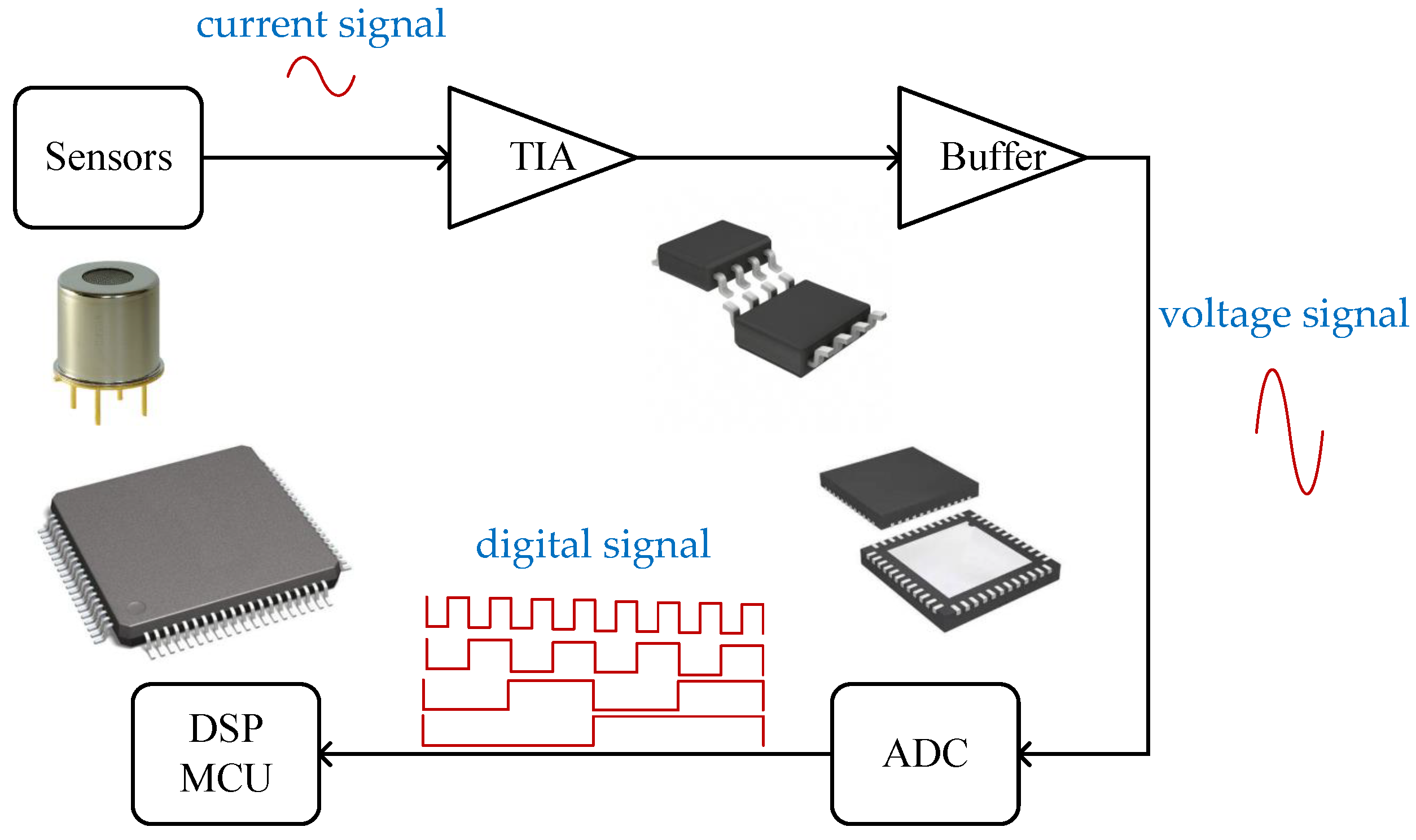
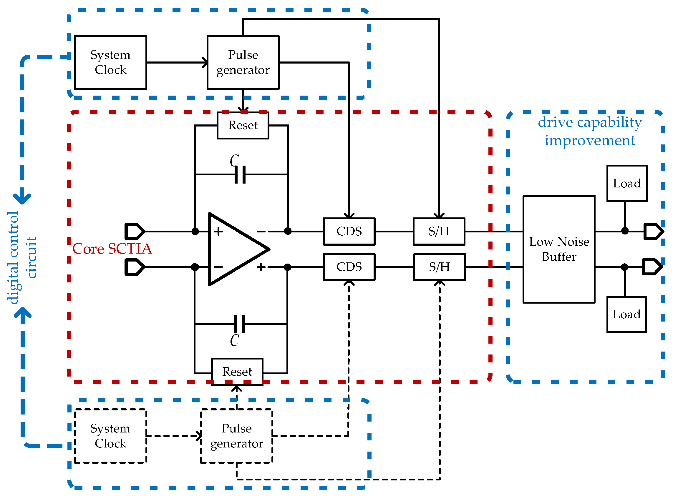
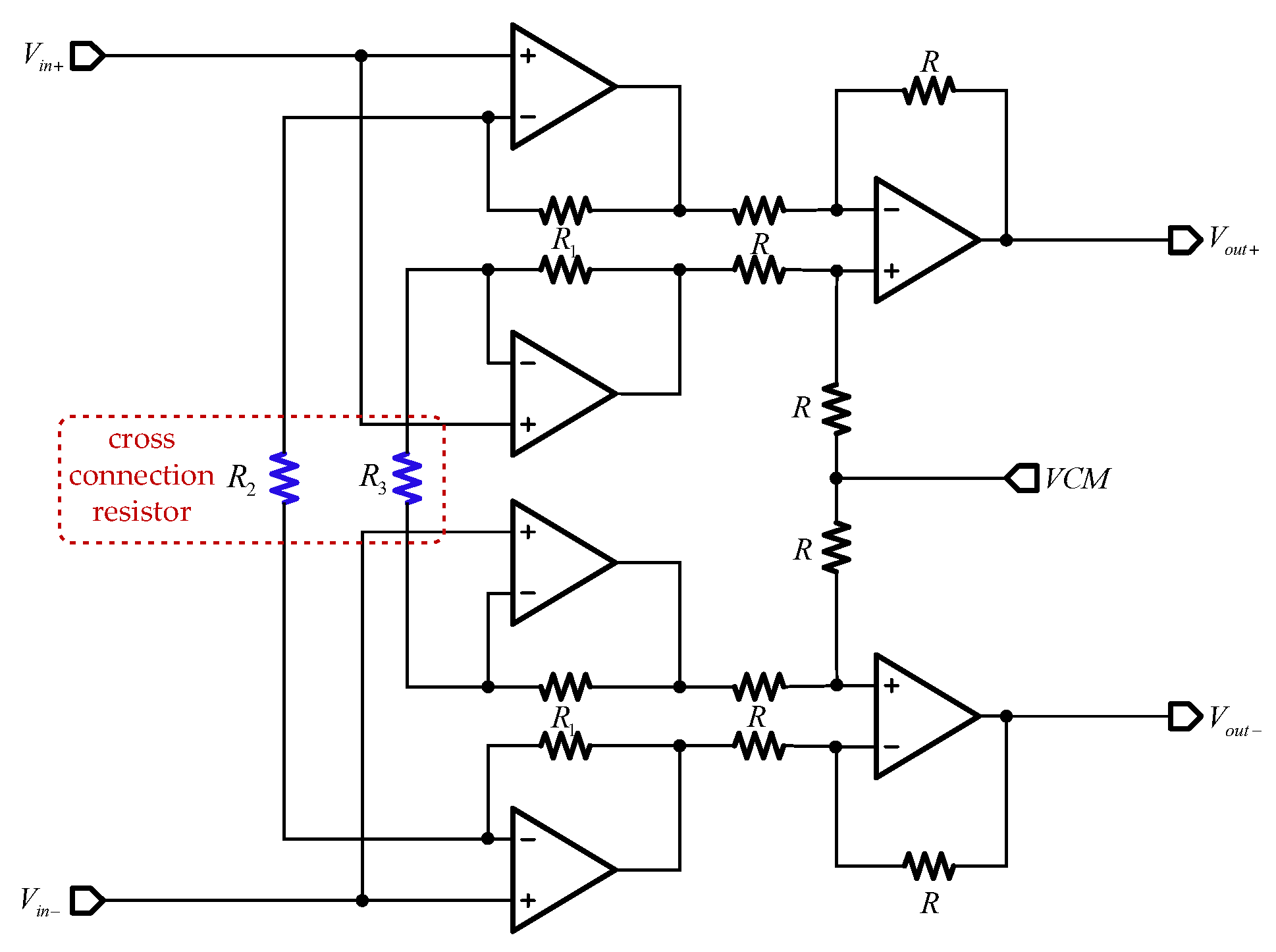
2.1. The Architecture Design

Figure 2 shows the architecture of the current detection system. It consists of a TIA adopting switched-capacitors, CDS, digital circuit controlling switches, and a low noise buffer employed to improve the drive capability.

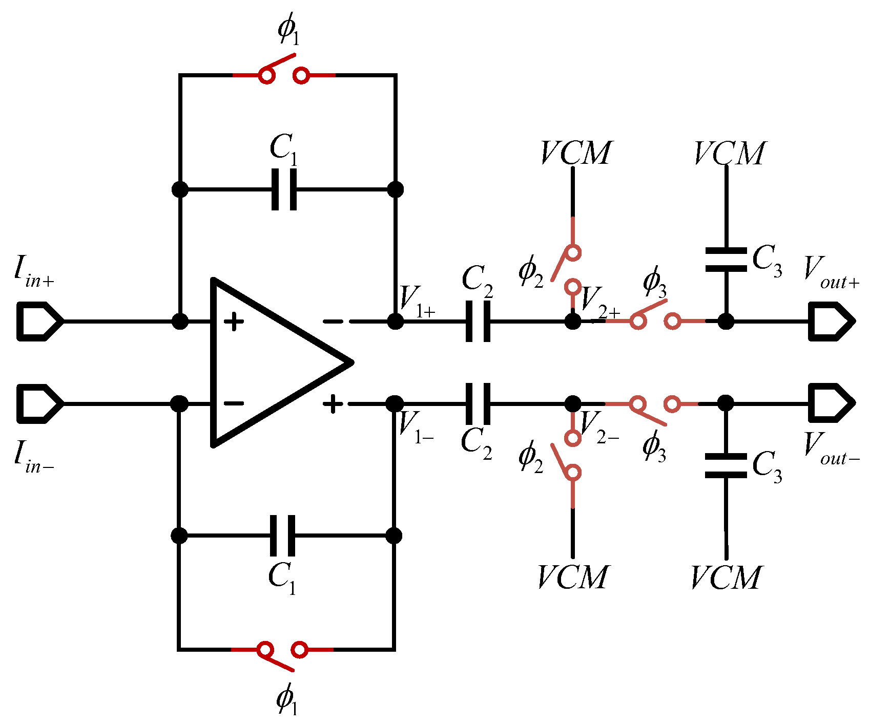
2.2. The Introduction to SCTIA

As present in Figure 3, the TIA contains a fully differential operational amplifier, several capacitors used for different functions, some switches, and a logic circuit used to control the switches and not displayed in the circuit diagram. All switches turn on (off) at high (low) voltage.
The timing phase generated to control the switches should be appropriate to make the circuit work properly. This paper employs the timing phases as shown in Figure 4.
As shown in Figure 4, there are three phases named φ 1 , φ 2 , and φ 3 , which control the switches named ϕ 1 , ϕ 2 , and ϕ 3 in Figure 5, respectively. The working period is marked as T in Figure 4.
When ϕ 1 is on, the voltages of C 1 and C 2 are reset to zero so that there is no charge on C 1 and C 2 . When ϕ 1 goes off at t 2 , the input current begins to charge C 1 , v 1 + , and v 1 starts to rise (fall) or fall (rise) until the next period comes. After ϕ 2 is off at t 3 , v 2 + , and v 2 follow the change of v 1 + and v 1 , respectively. Sample and hold circuit, consisting of a CMOS switch ϕ 3 and a sample capacitor C 3 , is used to sample v 2 at the end of t 5 and hold the value until the next time when ϕ 3 is on. The brief waveforms of the node voltage of the TIA are shown in Figure 6 [20].

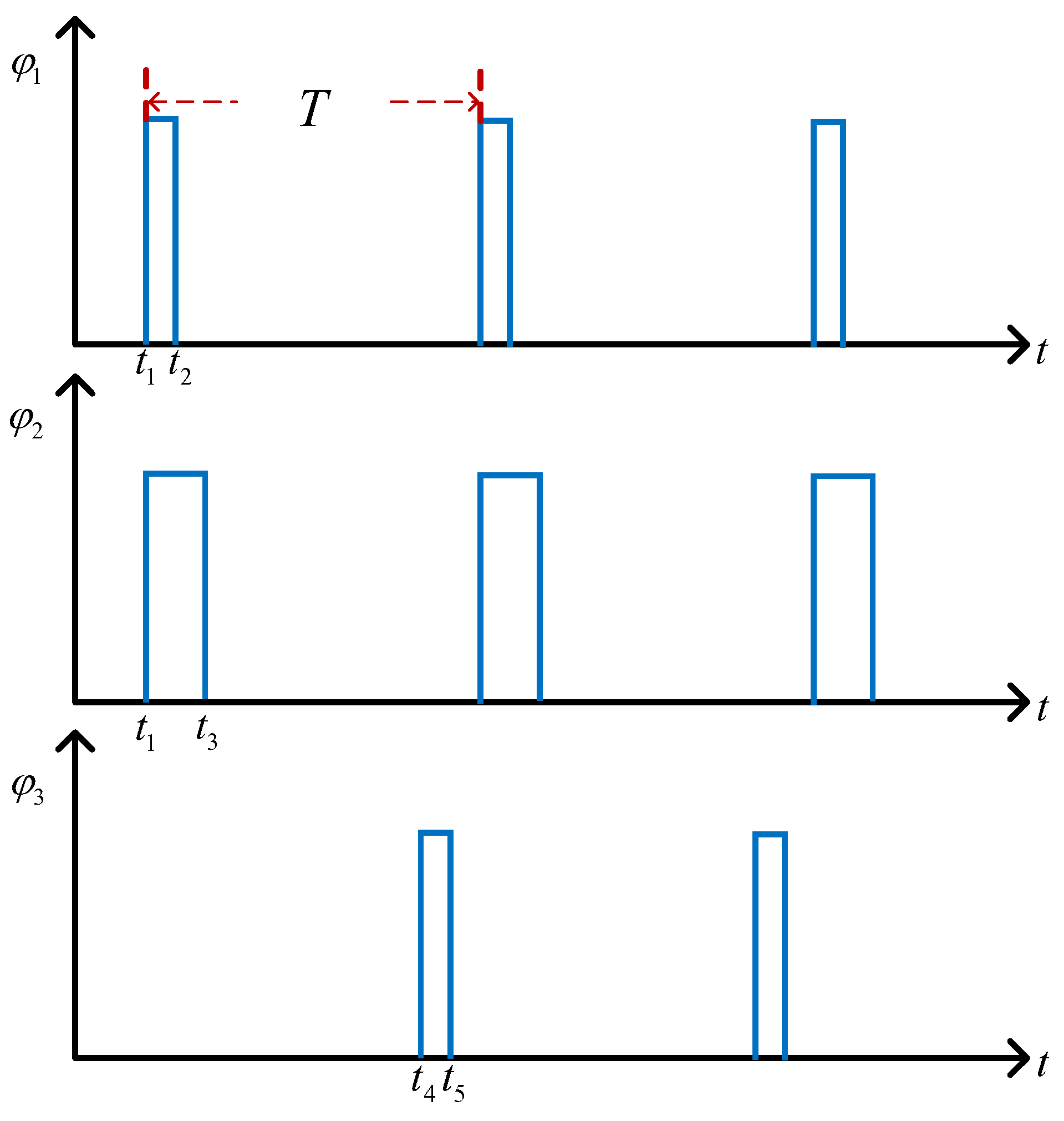
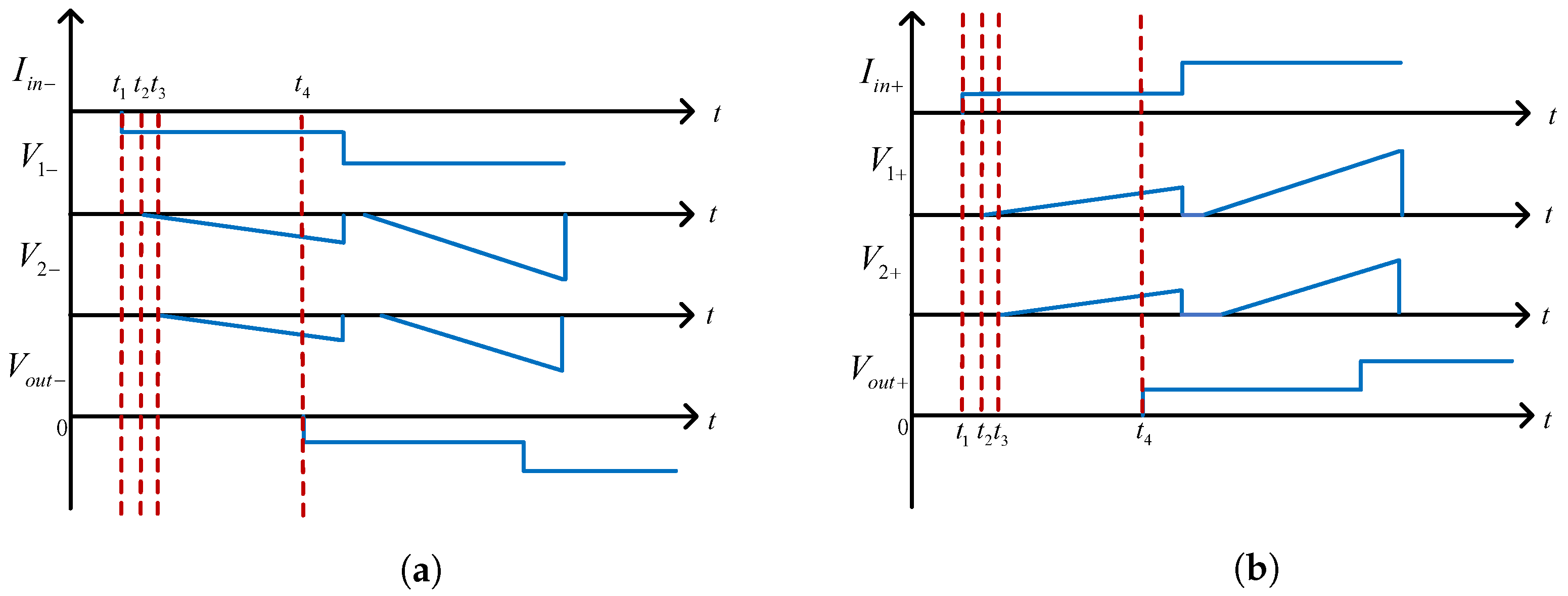
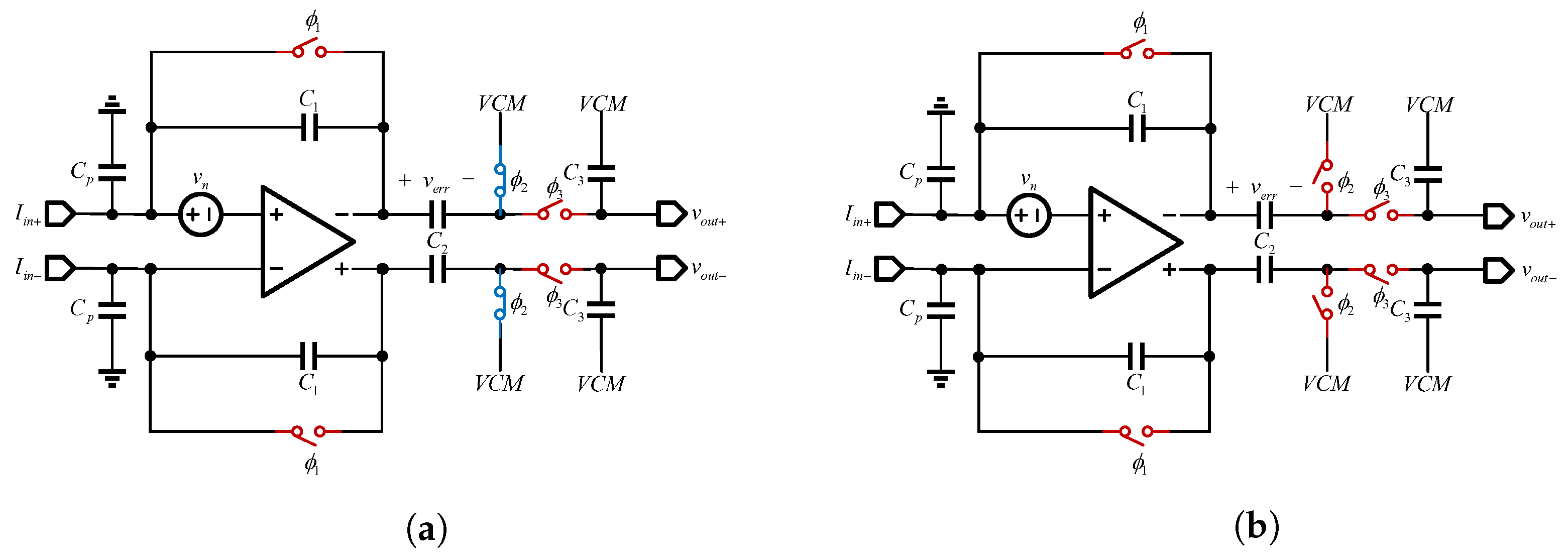
2.3. Correlated Double Sampling

The input-referred noise current is required to be small enough to make the TIA have the capability of detecting weak current signals.
Compared with the topology of resistive feedback, there is no resistor used in the structure of SCTIA, and then we can conclude the noise sources in the circuit. The noise sources of the TIAs are flicker noise, thermal noise of the operational amplifier, noise from the clock phase, and the shot noise caused by the leakage currents of the Electro-Static Discharge (ESD) protection diodes at the input of TIA, which is on the order of f A during regular operation. Since the transistors of switches work in the deep linear region, the clock noise is greatly reduced. Consequently, the noise from the Opamp usually dominates other noise sources. CDS is a technique commonly applied to reduce the noise of operational amplifiers, especially utilized for flicker noise and offset cancellation [20].
Signify the sum of the offset and low-frequency noise, principally flicker noise, as shown in Figure 7. To simplify the analysis, assume that v n exists only at the positive port of the amplifier.
At the time of t 3 as shown in Figure 8, v n ( t 3 ) , denotes the voltage of v n at t 3 , is amplified by the operational amplifier and the amplification coefficient depends on the ratio of parasitic capacitance C p and feedback capacitance C 1 and stored in C 2 as a voltage v e r r across C 2 .
It is effortless to get the expression of v e r r as shown in the following.
v e r r ( t 3 ) = 1 + C p C 1 v n ( t 3 ) .
When all switches are off, charges stored in C 2 will not be variational for one end of C 2 connected to high resistance, like a floating state. Obviously, v 1 + , at t 5 , can be expressed as
v 1 + = v e r r ( t 5 ) + v s i ( t 5 ) .
v s i ( t 5 ) denotes the signal when noise is going to be omitted. Compared with a clock signal, the frequency of v n is much smaller, for that v n is mainly comprised of offset and flicker noise of the Opamp. Then it is reasonable to regard v n as a constant in a single period so that the effect of offset and flicker noise at the output can be canceled through the above technology [21].

3. Detailed Analysis

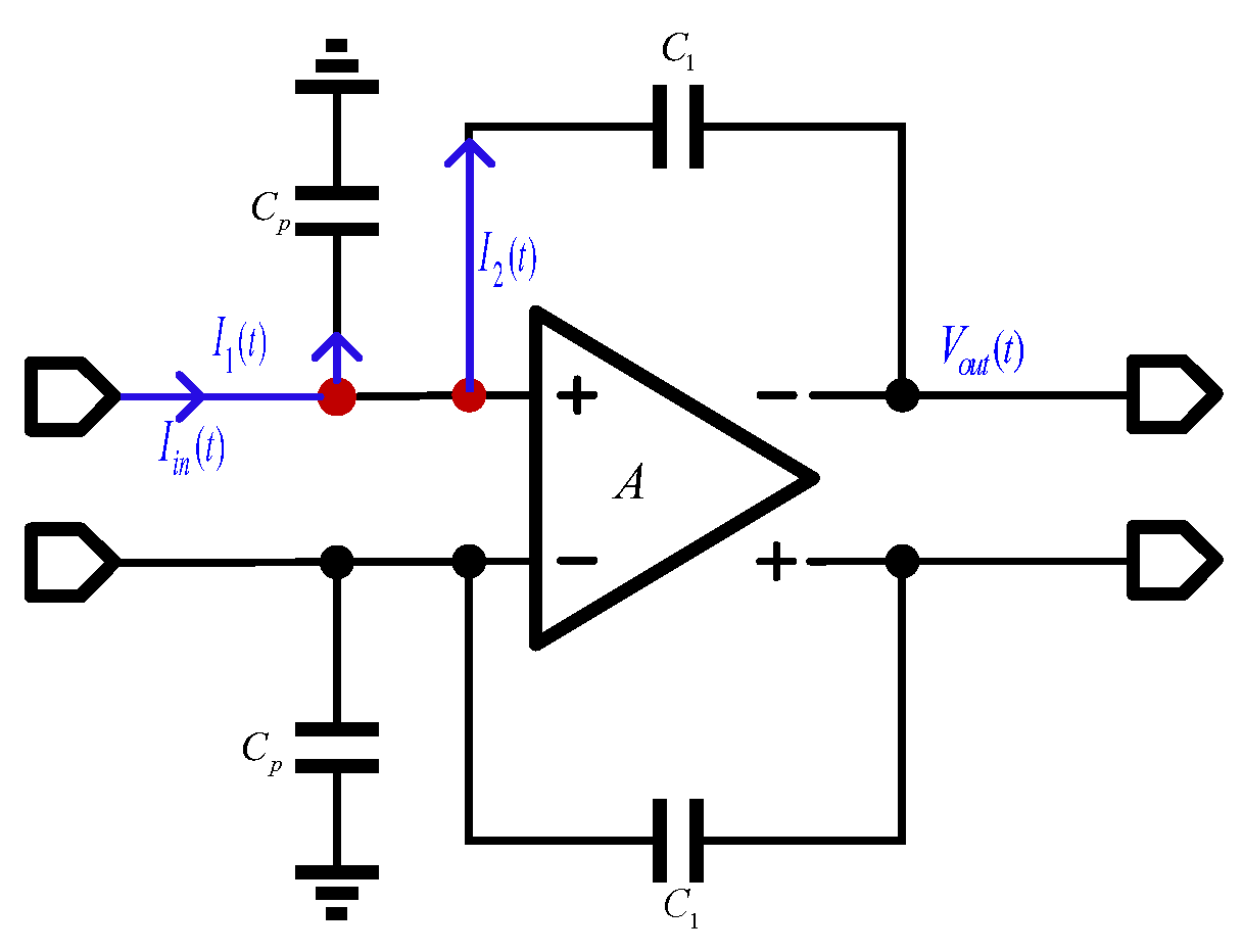
3.1. The Charge Distribution Model

In the previous sections, we have introduced the working principle of TIA briefly. An analysis in detail of the circuit is needed to be carried out to guide the actual design. We can derive the equations which describe the working process according to the following analysis based on charge distribution.
When ϕ 1 is on, the input and the output of the Opamp are connected directly, and then the charge on the feedback capacitor C 1 and capacitor C 2 is zeroed. Compared with the branch of the capacitor, the output of the Opamp shows lower impedance, so the input current flows into the output stage of the Opamp through the feedback switch directly, then v 1 + and v 1 are expressed below.
v 1 + = 0 ,
v 2 + = 0 .
To simplify the analysis, the differential terminals v 1 and v 2 are omitted. The same goes for the following analysis. Since the sampling switch is not closed, v o u t + remains unchanged as a value as the previous period v o u t + was.
When ϕ 1 is off and ϕ 2 is still on, the input current will charge C 1 . At the moment switch ϕ 1 is off, feedback capacitor C 1 , which was originally shorted, is connected to the circuit, and then the load state of the operational amplifier will change. The voltage of the input and output of the amplifier will not mutate for both the charge stored in C 1 and C 2 at the moment before and after the switch ϕ 1 is off is zero.
An Opamp has the character of a virtual short circuit and virtual open circuit for its high gain and high input impedance. As a result, the input current flow from the input node to the output node of the amplifier through the feedback capacitor will not make the voltage of the input node of the amplifier change. According to the relationship between voltage and current of the capacitors, the voltage of C 1 can be expressed as
u c 1 ( t ) = 1 C 1 t 2 t i i n ( t ) d t + u c 1 ( t 2 ) .
where t 2 t t 3 , u c 1 ( t 2 ) = 0 .
Compared with the period of the clock, the period of the input current is longer. As a result, it is reasonable to regard the input current i i n ( t ) as a constant I i n , so that the above expression can be simplified as
u c 1 ( t ) = t t 2 C 1 I i n .
That t 2 t t 3 is assumed. The voltage of the output of the Opamp varies linearly concerning the input current over time. Since the voltage of the output of the amplifier has changed, and another port of capacitor C 2 is connected to V C M , current will flow through capacitor C 2 , whose value depends on the rate of change of the output voltage of the Opamp. According to the expression of u c 1 ( t ) , the current which flows through capacitor C 2 can be calculated below.
i C 1 = C 2 d u 2 d t = C 2 I i n C 1 .
According to Kirchhoff’s Current Law (KCL), the output current of the Opamp is required to be larger than the sum of current flowing through the capacitor C 1 and capacitor C 2 .
When ϕ 1 , ϕ 2 , ϕ 3 all are off, the port of capacitor C 2 connected to switch ϕ 3 is considered to be in a high resistance state, as a consequence, there is no current flow through capacitor C 2 , so that the voltage of the two ports of C 2 do not change, v 2 is going to change as v 1 changes.
The expression of v 1 + and v 2 + can be derived as follows when t 3 t t 4 .
v 1 + = 1 C 1 t 2 t i i n + ( t ) d t + u c 1 ( t 2 ) ,
v 2 + = 1 C 1 t 3 t i i n + ( t ) d t .
Assuming that the output voltage of the TIA is V ( n T T ) at the end of the last cycle, as a result, charges stored in capacitor C 3 at t 4 can be expressed as
Q C 31 = V ( n T T ) C 3 .
During the phase when ϕ 1 is off, and ϕ 2 is on, charges stored in C 2 at t 4 can be derived as
Q C 21 = i i n ( t 3 t 2 ) C 3 .
That t 4 denotes the moment before ϕ 3 is on.
The voltage of a capacitor does not change dramatically since C 1 is connected across the input and output of the Opamp, which means that the voltage at the node where the C 1 is connected to the input of the Opamp remains zero.
Suppose that the final stable output at the end of the period is V ( n T ) , and V ( n T ) > V ( n T T ) . According to the analysis above, we can derive v 2 as
v 2 = I i n C 1 ( t 4 t 3 ) .
The charging process when the switch ϕ 3 is on is analyzed separately to simplify the analysis. As a result, the voltage across C 1 is regarded as constant during the process of charge redistribution between C 2 and C 2 .
Given the assumption of V ( n T ) > V ( n T T ) , the charge will be transferred from capacitor C 2 to capacitor C 3 when the redistribution of charge happens. In other words, v 1 will drop sharply, and then v 1 will drop sharply as well. The voltage of the input of the Opamp connected to capacitor C 1 changes in the same way as v 1 . Through the adjustment of the feedback of the Opamp, the input voltage of the amplifier will change to zero, and the output voltage of the amplifier will return to I i n / C 1 ( t 4 t 2 ) , during the above process, the charge is transferred.
Before and after the transfer of charge, the amount of charge is conserved, so the charges stored in capacitor C 2 and C 3 have the relationship as follows.
( V ( n T ) i i n ( t 4 t 2 ) C 1 ) C 2 + V ( n T ) C 3 = ( V ( n T T ) ) C 3 + i i n ( t 3 t 2 ) C 1 C 2 ,
V ( n T ) = V ( n T T ) C 3 C 2 + C 3 + C 2 C 1 ( C 2 + C 3 ) i i n ( t 4 + t 3 2 t 2 ) .
For the assumption of V ( n T ) > V ( n T T ) , we can define V n T T = α V n T , where 0 < α < 1 , so that the trans-impedance gain of the TIA can be derived as
V ( n T ) i i n = C 2 [ C 2 + ( 1 α ) C 3 ] C 1 ( t 4 + t 3 2 t 2 ) .

3.2. Equivalent Load Capacitance

In order to optimize the power consumption, it is necessary to know the load state of the Opamp at each phase. Figure 9 is the different working states of the TIA. In separate circuit states, capacitors connected to the output of the Opamp are dissimilar. According to the method concluded in [22], the equivalent load capacitances of the Opamp at different phases are expressed below.
C e q a = C p + C 2 ,
C e q b = C p + C 2 ( 1 + C p / C 1 ) ,
C e q c = C p ,
C e q d = C p + ( C 2 / / C 3 ) ( 1 + C p / C 1 ) .
According to the equations above, it is clear that when ϕ 2 is on and ϕ 1 is off, the load capacitance of the Opamp is the largest.

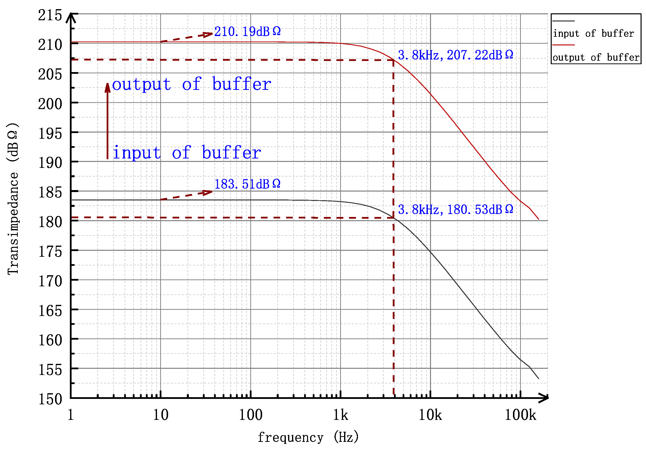
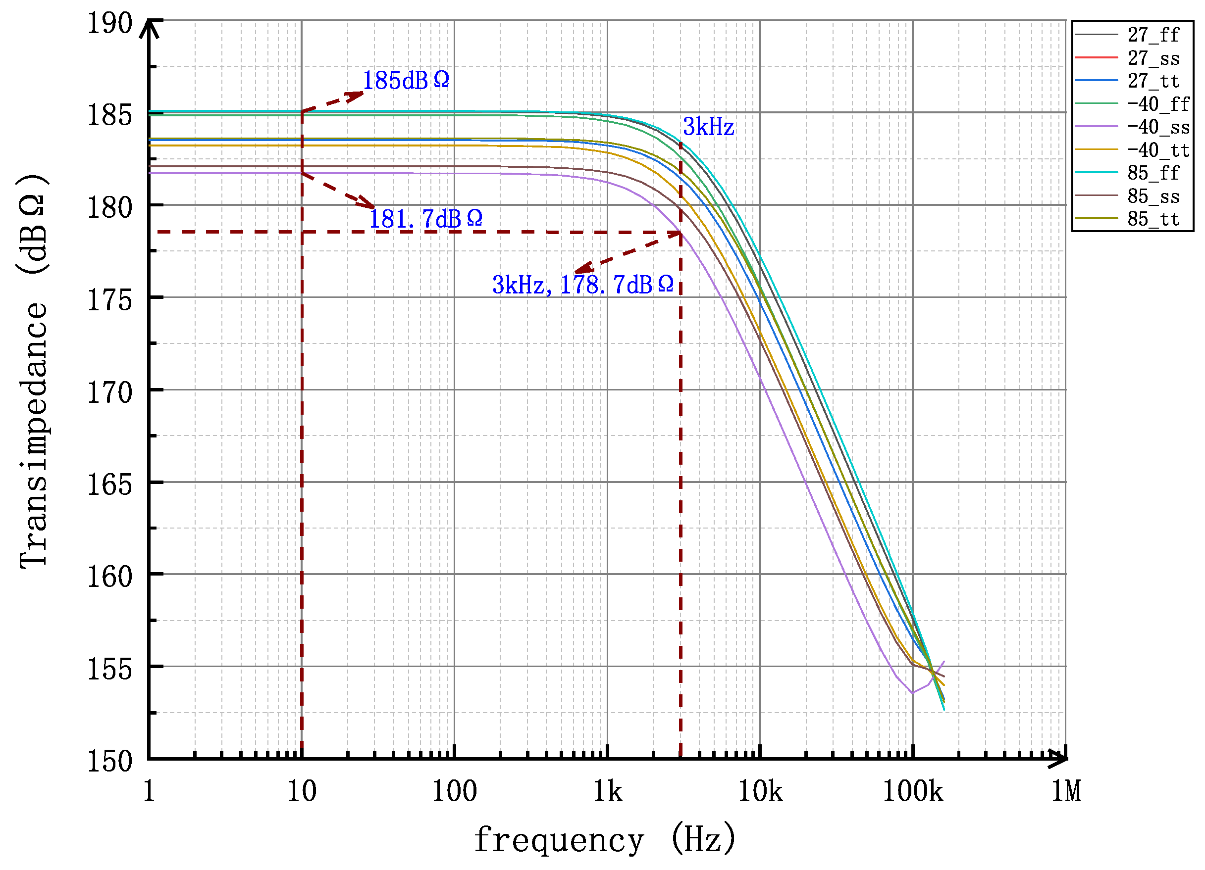
3.3. Analysis of Bandwidth

Different from the analysis in conventional circuit structures, it is hard to analyze the bandwidth in SCTIAs accurately, but the factors affecting the bandwidth can be obtained through qualitative analysis.
Because of switch capacitors, there is a hypothesis about the trans-impedance gain—that the input current is regarded as a constant in a complete working period in the above analysis. To satisfy the assumptions, the bandwidth of the TIA is far less than the frequency of a complete working cycle.
As a consequence, we can improve the bandwidth of the TIA through the method of increasing the frequency of the system clock, which will decrease the charging time of capacitor C 1 in a single cycle, the trans-impedance gain will decline. In addition, the time when switch ϕ 1 is closed becomes shorter, and the power consumption of the Opamp is required to be higher to meet the quick setting up under the condition of unit feedback. Therefore, the system clock should be reasonable according to the trade-off of power, bandwidth, and trans-impedance gain.
In addition to a constraint on bandwidth from the system clock, the pole generated by the equivalent resistance and the input capacitor also has an impact on the bandwidth. Since the frequency of this pole is relatively high, it is generally not taken into account when the requirement of bandwidth is low.

3.4. Analysis of Leakage Current

In the sub- p A current detection circuit, the leakage current needs to be concerned. In CMOS technology, it is considered that leakage of PN junction and leakage of MOS operating in the sub-threshold region are the primary leakage current in the circuit [23].
The leakage current of the PN junction is caused by the drift of minority carriers at the edge of the depletion region and the recombination of electron–hole pairs in the depletion region. Generally, the leakage current of PN junction in 0.18 μm CMOS technology is in the order of aA/μm2, which is a low leakage current level in the CMOS circuit [24,25].
The leakage current of MOS operating in the sub-threshold region is generated by the channel between source and drain when the gate-source voltage is less than the threshold voltage, which is mainly determined by the diffusion of carriers [26].
Some secondary effects of MOS, such as DIBL (Drain Induced Barrier Lowering), body effect, and threshold voltage roll-off, will affect the threshold of MOS and then influence the sub-threshold leakage current of MOS [27]. DIBL often occurs in small size devices because of the decrease in channel length, increasing the voltage at the drain. The source and drain depletion zone will close together. As a result, the number of electrons injected into the channel from the source will increase, resulting in an increase in leakage current. It is obvious that we can increase the length of the MOS to reduce the effect of DIBL on leakage current. Body effect is caused by different potentials of bulk and source, and it will change the threshold voltage of the MOS. It is a good method to take advantage of the body effect to increase the threshold voltage of the MOS and then decrease leakage current [28]. Threshold voltage roll-off is caused by short channel length as DIBL. The typical sub-threshold leakage current of MOS is several decades f A of orders [29].

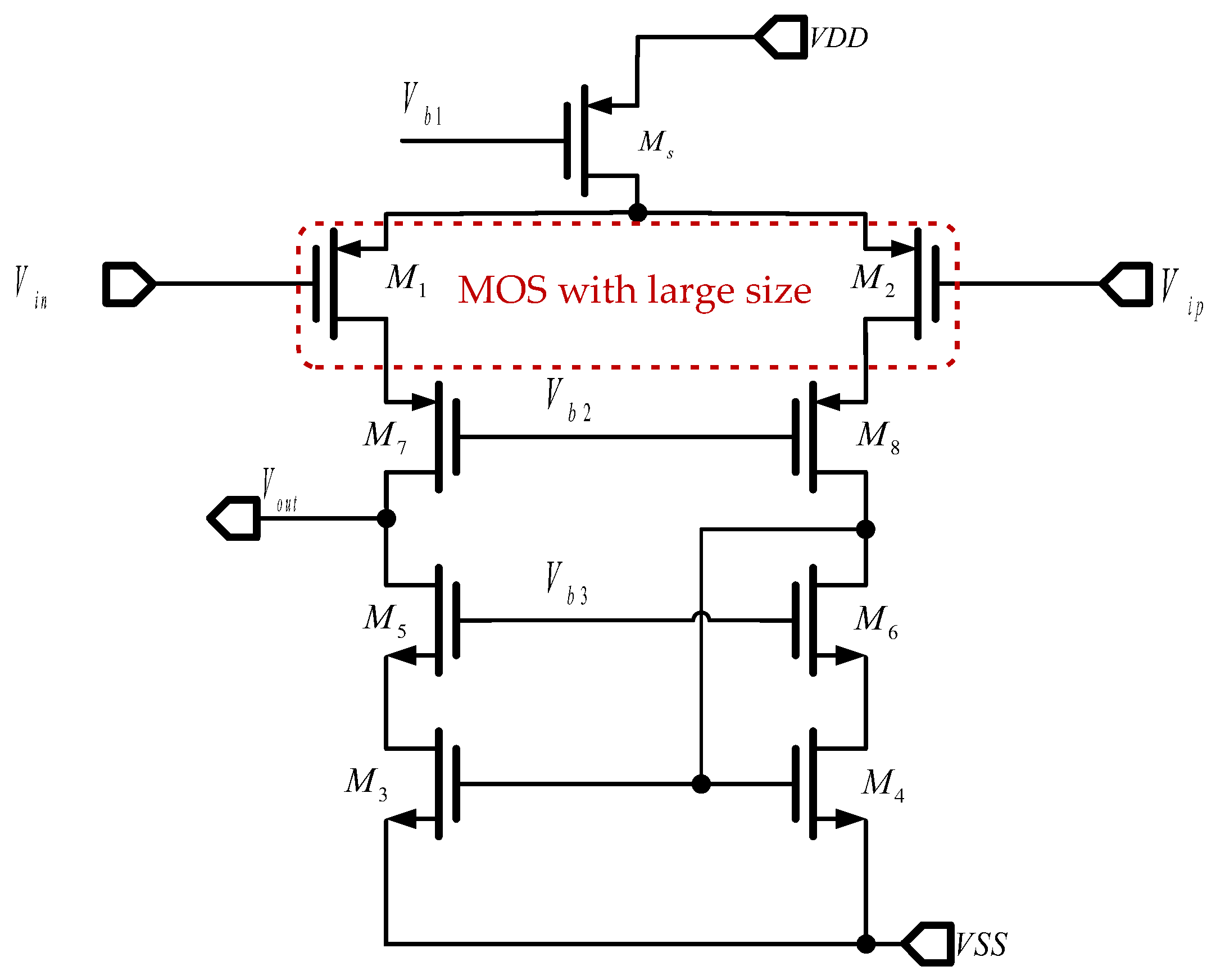
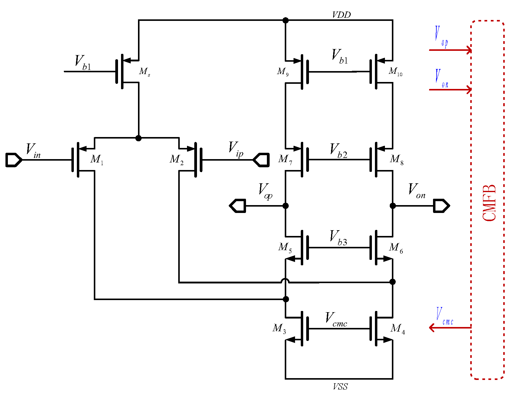
3.5. Effects of the Operational Amplifier on TIA

It is obvious to be seen from the above analysis that we can converse current signal to voltage signal because of the charging of the feedback capacitor C 1 . It is necessary to analyze the transient process when considering the influences of the Opamp, for the reason that the amplifier is the core element in the TIA.
The following equations hold at both the input and output of the Opamp.
I i n ( t ) = I 1 ( t ) + I 2 ( t ) ,
V i n ( t ) A = V o u t ( t ) ,
V o u t ( t ) V i n ( t ) = 1 C 1 I 2 ( t ) ( t 0 ) ,
V i n ( t ) = I 1 ( t ) t C p .
where I i n ( t ) is the input current, I 1 ( t ) is the current flowing through the parasitic capacitor C p , I 2 ( t ) is the current flowing through the feedback capacitor C 2 , V i n ( t ) is the voltage at the input of the Opamp, and V o u t ( t ) is the voltage at the output of the Opamp, all are shown in Figure 10. According to above equations, the relationship between V o u t ( t ) and I i n ( t ) can be derived as follows.
V o u t ( t ) I i n ( t ) = t C 1 1 1 + 1 / A + C p / ( A C 1 ) .
The gain of the Opamp A is required to be large enough to avoid the influence of the parasitic capacitor on trans-impedance gain.
Compared with telescopic cascade and two-stage amplifier, folded cascade amplifier has a better trade-off in power consumption and output swing. In this design, we adopt the structure of folded cascade amplifier, and the diagram is shown in Figure 11. Compared with NMOS, PMOS has lower flicker noise because the probability of capturing and releasing carriers is much smaller. Therefore, it is reasonable to choose PMOS as the input MOS of the amplifier.

3.6. Buffer Design

The TIA has a poor ability to drive load since its output is capacitive. Therefore, the TIA needs to be connected to an appropriate buffer to drive a load. In this paper, cross-connection technology is adopted to design a fully differential buffer with high input impedance and low output impedance based on telescopic operational amplifiers. The structure of the buffer is shown in Figure 12.
The relationship between the output and the input of the buffer can be derived as follows [30].
V o u t V i n = 2 × ( R 1 R 2 R 1 R 3 ) .
To reduce the overall power consumption, Opamps adopting a telescopic cascade structure, as shown in Figure 5, are applied to build the low noise buffer. For the reason that there are sampling capacitors at the output of the core TIA, the signal at the output will change due to the effect of clock feedthrough and charge injection of switches if low noise technology like chopper or auto-zero is adopted to reduce input-referred noise voltage of buffer. As a result, it is necessary to increase the size of the input MOS of the buffer to achieve the requirement of low noise, as described in Figure 5.

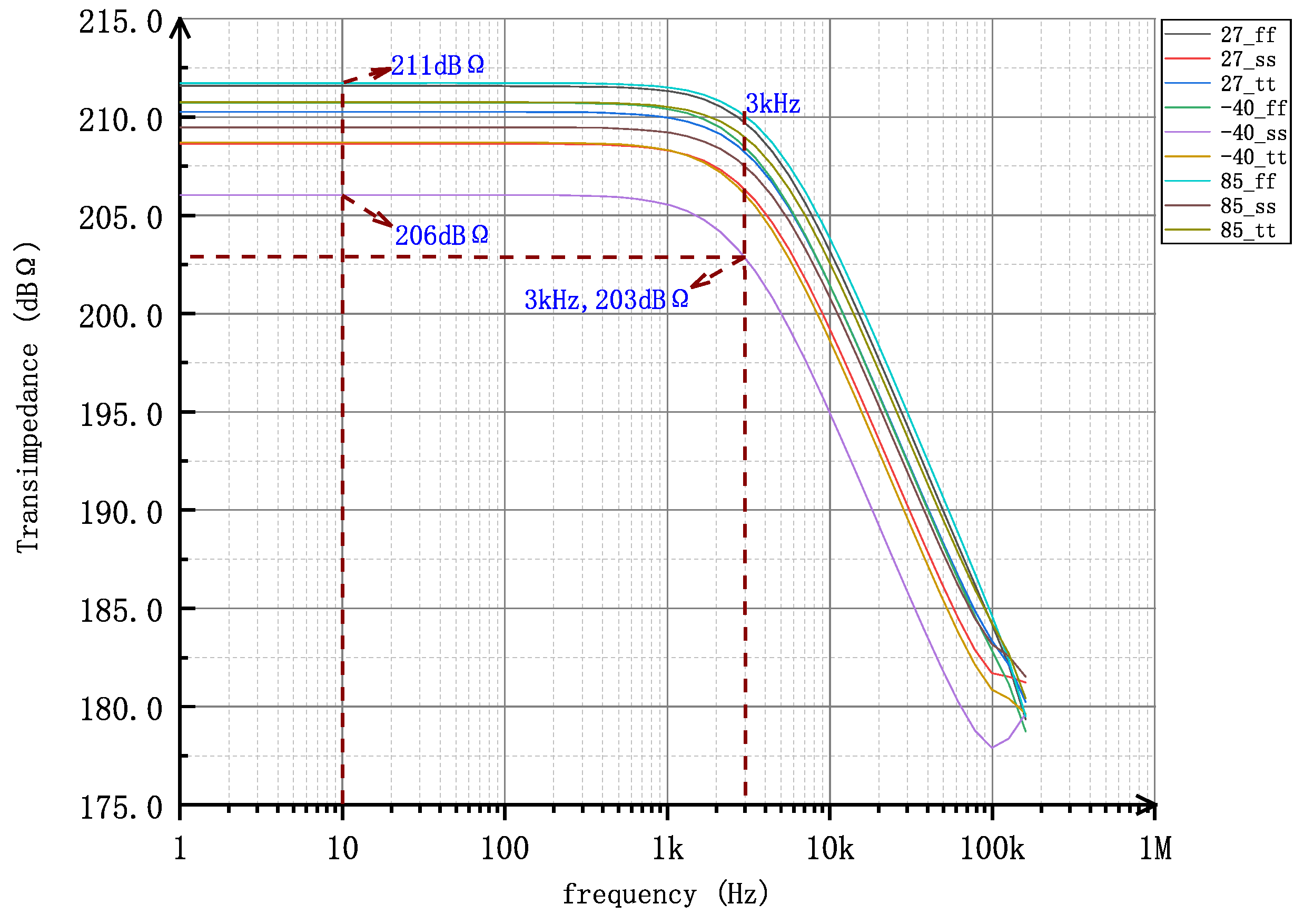
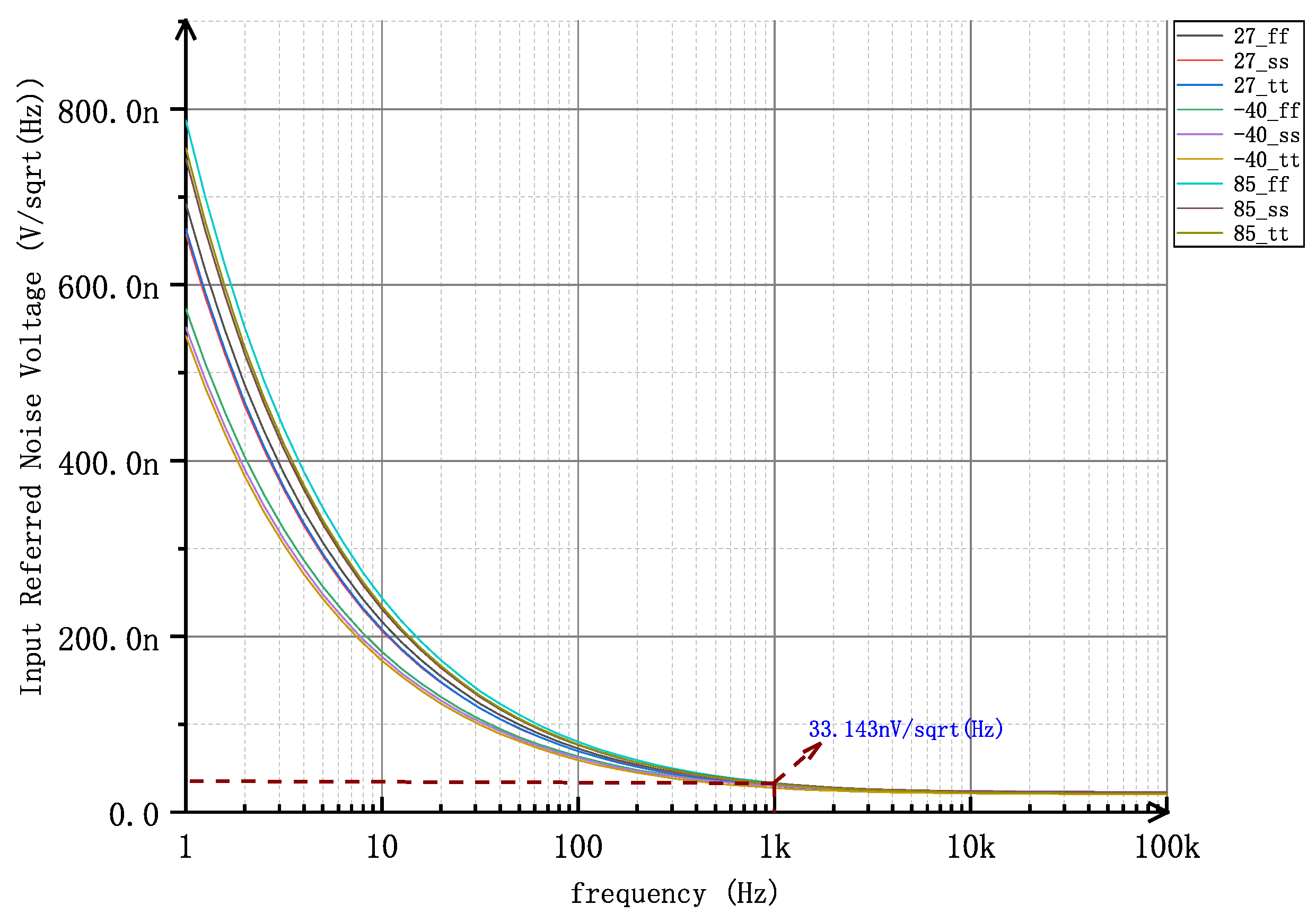
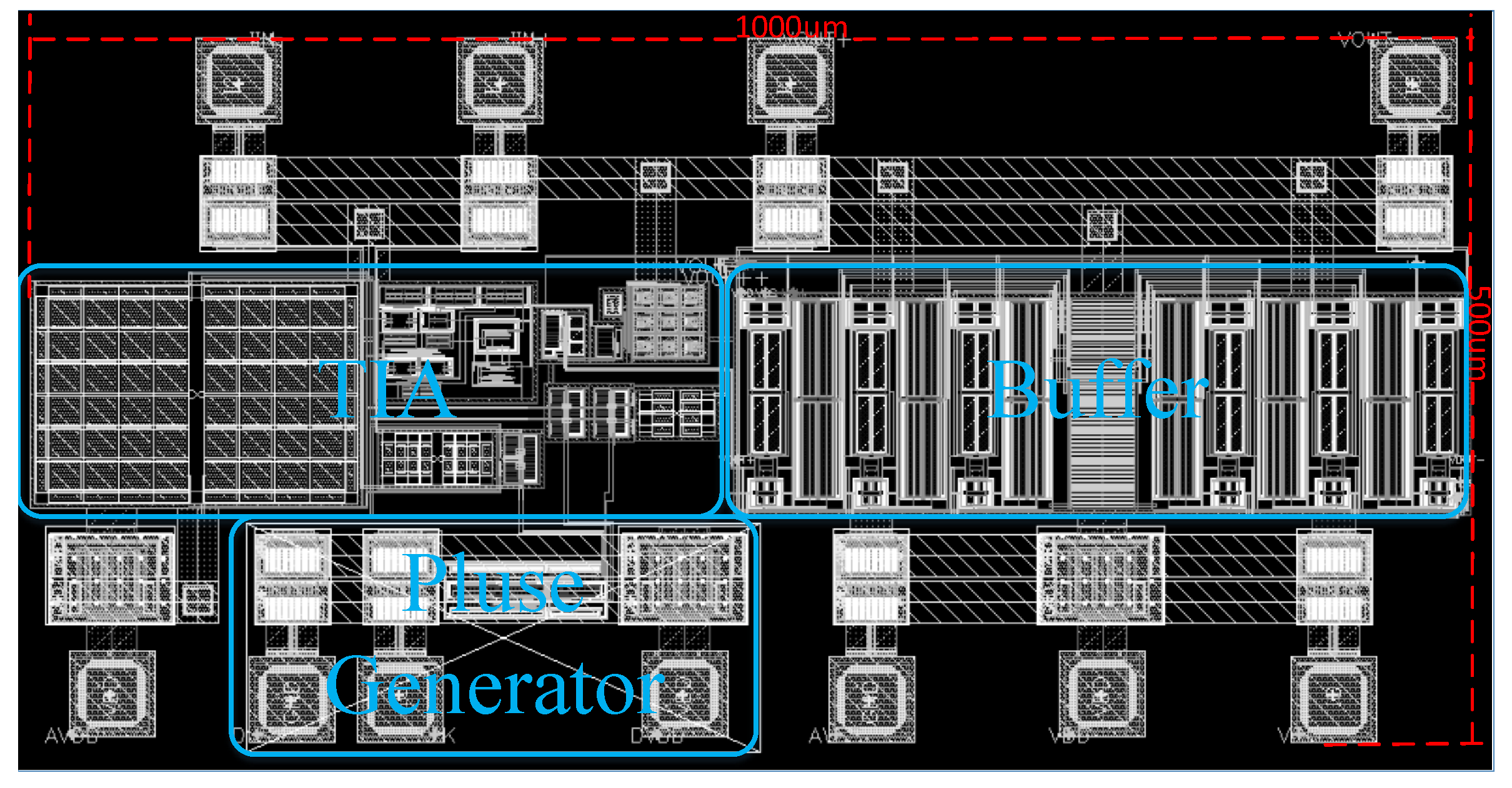
4. Result and Analysis

The frequency response and noise performance of the TIA have been simulated. We can obtain the periodic operating point of the TIA through “Periodic Steady State” (PSS) analysis. After PSS is completed, “Periodic Alternating Current” (PAC) analysis computes the frequency response of the TIA, and “Periodic Noise” (PNOISE) analysis is run to find out its noise behavior.
That shown in Figure 13 and Figure 14 are the results representing the gain of the input and output nodes of the buffer.
Low-frequency trans-impedance gains as high as 206 dB with a 3 kHz–3 dB bandwidth at the output node of the buffer and 183 dB with a 3 kHz bandwidth at the input node of the buffer have been simulated in the worst case from the result. This shows that the gain of the in-band signal is very high, and the designed current readout circuit has a good ability to amplify the tiny current.
The curves of the frequency response are shown in Figure 8 under the condition of 27 °C and “typical–typical” (tt) process corner to facilitate the comparison of the input and output gains of the buffer. The gain is observed to increase from 183.51 dBΩ to 210.19 dBΩ, indicating that the buffer could improve the ability to drive loads and enhance the gain of the trans-impedance amplifier.
Figure 15 displays the input-referred noise voltage of the buffer. In this paper, the low-frequency input-referred noise voltage of the buffer is decreased through the increasing size of the input M O S . As shown in the result, input-referred noise voltage of 33.143 nV H z at 1 kHz has been achieved regardless of process and temperature variation.
That shown in Figure 16 is the performance of the input-referred noise current of the TIA. A low input-referred noise current of 2.69 f A / H z is achieved. Its noise performance ensures that the current readout circuit can amplify the weak current in the band effectively without introducing too much noise.
That shown in Figure 17 is the layout of the complete system, and all sub-circuits have been marked on the layout.
A comparison result of the performance of the published circuits in recent years is shown in Table 1.
From the comparison result, it is apparent that CT-TIAs (Continuous type trans-impedance amplifiers) [11,13,31,35] reach the M H z bandwidth, while DT-TIAs (Discrete type trans-impedance amplifiers) [20,33], including the design in this paper, are limited in bandwidth by system clock as analyzed in Section 3.3.
According to the conclusion drawn from the charge distribution model and equivalent load capacitance, the trans-impedance gain and power consumption of the design have been optimized.
This work has advantages in the performance of gain and power consumption compared with the previous work displayed in Table 1, so it is suitable for low-noise and low-power application scenarios with the relaxed bandwidth requirement, such as the current process in ECG, EGG, NIRS, and DNA analysis [36,37,38].

5. Conclusions

Building on previous work, in order to analyze the factors affecting the trans-impedance gain of SCTIAs accurately, the analytical model of charge distribution proposed improves the analysis theory of SCTIAs. Grounded on the proposed model, combined with the analysis of load states and effects on the trans-impedance gain of the Opamp, the designed circuit achieves a trans-impedance gain as high as 206 dB with 3 kHz bandwidth and 0.643 mW power consumption. Its input-referred noise current is as low as 2.69 f A / H z at 1 kHz. The simulation results show that the model is referential on low power and high gain TIAs. The detailed analysis process helps technical personnel, engineers, and researchers specializing in TIAs to design high-performance current readout circuits.

Author Contributions

Conceptualization, D.J., Q.S. and S.H.; methodology, D.J., Q.S., Z.W., Q.C.; software, D.J., Q.C., Z.L., J.X.; formal analysis, D.J., Z.W., S.H.; writing—original draft preparation, D.J., Q.C.; writing—review and editing, D.J., Q.C., S.H.; supervision, S.H. All authors have read and agreed to the published version of the manuscript.

Funding

This research was funded by the National Key R&D Program of China under grant number 2019YFB2204500.

Acknowledgments

The authors acknowledge professors and peers at the Institute of the Microelectronics of the Chinese Academy of Sciences and the University of Chinese Academy of Sciences for knowledge sharing.

Conflicts of Interest

The authors declare no conflict of interest.

Abbreviations

The following abbreviations are used in this manuscript:
ADCAnalog to Digital Converter
MCUMicro Control Unit
DSPDigital Signal Processor
TIATransimpedance amplifier
SCTIASwitched-capacitor transimpedance amplifier
OpampOperational amplifier
GBWGain-Bandwidth product
CDSCorrelated double sampling
ESDElectro-Static Discharge
KCLKirchhoff’s Current Law
CT-TIAsContinuous type trans-impedance amplifiers
DT-TIAsDiscrete type trans-impedance amplifiers
PSSPeriodic Steady State
PACPeriodic Alternating Current
PNOISEPeriodic Noise

References

  1. Kim, S.; Hwang, D.H.; Lee, H.; Han, S.K.; Cho, S. The effect of Micro-current electrical stimulation on muscle atrophy caused by sciatic nerve compression. In Proceedings of the 2019 International Conference on Electronics, Information, and Communication (ICEIC 2019), Auckland, New Zealand, 22–25 January 2019. [Google Scholar]
  2. Lagoumintzis, G.; Sideris, S.K.M.P.K.K.C.R.H. Wireless Micro Current Stimulation technology improves firework burn healing: Clinical applications of WMCS technology. In Proceedings of the 2014 4th International Conference on Wireless Mobile Communication and Healthcare—Transforming Healthcare Through Innovations in Mobile and Wireless Technologies (MOBIHEALTH 2014), Athens, Greece, 3–5 November 2014; pp. 172–175. [Google Scholar]
  3. Farwell, L.A.; Richardson, D.R.G.F.J. Brain fingerprinting classification concealed information test detects US Navy military medical information with P300. In Proceedings of the FNINS. 2014. Available online: https://www.frontiersin.org/articles/10.3389/fnins.2014.00410/full (accessed on 1 May 2022).
  4. Ying, M.; Li, Z. Analysis of current situation of the frequent food safety accidents and its reasons in China. In Proceedings of the 2011 International Conference on Computer Science and Service System (CSSS 2011), Nanjing, China, 27–29 June 2011; pp. 3864–3867. [Google Scholar] [CrossRef]
  5. Ullah, M.N.; Park, Y.; Kim, G.B.; Kim, C.; Park, C.; Choi, H.; Yeom, J.Y. Simultaneous Acquisition of Ultrasound and Gamma Signals with a Single-Channel Readout. Sensors 2021, 21, 1048. [Google Scholar] [CrossRef]
  6. Garrou, P. Wafer level chip scale packaging (WL-CSP): An overview. TADVP 2000, 23, 198–205. [Google Scholar] [CrossRef]
  7. Li, D.; Minoia, G.; Repossi, M.; Baldi, D.; Temporiti, E.; Mazzanti, A.; Svelto, F.D. A Low-Noise Design Technique for High-Speed CMOS Optical Receivers. IEEE J. Solid State Circuits 2014, 49, 1437–1447. [Google Scholar] [CrossRef]
  8. Park, S.M.; Yoo, H.J.D. 1.25-Gb/s regulated cascode CMOS transimpedance amplifier for Gigabit Ethernet applications. IEEE J. Solid State Circuits 2004, 39, 112–121. [Google Scholar] [CrossRef] [Green Version]
  9. Ferrari, G.; Gozzini, F.; Molari, A.; Sampietro, M. Transimpedance Amplifier for High Sensitivity Current Measurements on Nanodevices. IEEE J. Solid State Circuits 2009, 44, 1609–1616. [Google Scholar] [CrossRef]
  10. Sackinger, E.; Circuits, E.D. The Transimpedance Limit. IEEE Trans. Circuits Syst. Regul. Pap. 2010, 57, 1848–1856. [Google Scholar] [CrossRef]
  11. Lei, K.; Heidari, H.; Mak, P.; Law, M.; Maloberti, F. Exploring the noise limits of fully-differential micro-watt transimpedance amplifiers for Sub-pA/yHz sensitivity. In Proceedings of the 2015 11th Conference on Ph.D. Research in Microelectronics and Electronics (PRIME 2015), Glasgow, UK, 29 June–2 July 2015; pp. 290–293. [Google Scholar] [CrossRef]
  12. Salvia, J.; Lajevardi, P.; Hekmat, M.; Murmann, B. A 56MΩ CMOS TIA for MEMS applications. In Proceedings of the IEEE Custom Integrated Circuits Conference (CICC 2009), San Jose, CA, USA, 13–16 September 2009. [Google Scholar]
  13. Ferrari, G.; Gozzini, F.; Sampietro, M. A Current-Sensitive Front-End Amplifier for Nano-Biosensors with a 2MHz BW. In Proceedings of the Solid-State Circuits Conference, ISSCC 2007, San Francisco, CA, USA, 11–15 February 2007; Digest of Technical Papers. IEEE International: Piscataway, NJ, USA, 2007. [Google Scholar]
  14. Bianchi, D.; Ferrari, G.; Rottigni, A.; Sampietro, M. CMOS Impedance Analyzer for Nanosamples Investigation Operating up to 150 MHz With Sub-aF Resolution. IEEE J. Solid State Circuits 2014, 49, 2748–2757. [Google Scholar] [CrossRef]
  15. Chuah, J.H.; Holburn, D. Design of Low-Noise High-Gain CMOS Transimpedance Amplifier for Intelligent Sensing of Secondary Electrons. IEEE Sens. J. 2015, 15, 5997–6004. [Google Scholar] [CrossRef]
  16. Tajalli, A.; Leblebici, Y.; Brauer, E.J. Implementing ultra-high-value floating tunable CMOS resistors. Electron. Lett. 2008, 44, 349–350. [Google Scholar] [CrossRef] [Green Version]
  17. Djekic, D.; Fantner, G.; Behrends, J.; Lips, K.; Ortmanns, M.; Anders, J. A transimpedance amplifier using a widely tunable PVT-independent pseudo-resistor for high-performance current sensing applications. In Proceedings of the 43rd IEEE European Solid State Circuits Conference(ESSCIRC 2017), Leuven, Belgium, 11–14 September 2017; pp. 79–82. [Google Scholar] [CrossRef] [Green Version]
  18. Crescentini, M.; Bennati, M.; Carminati, M.; Tartagni, M. Noise Limits of CMOS Current Interfaces for Biosensors: A Review. IEEE Trans. Biomed. Circuits Syst. 2014, 8, 278–292. [Google Scholar] [CrossRef]
  19. Djekic, D.; Häberle, M.; Mohamed, A.; Baumgärtner, L.; Anders, J. A 440-kOhm to 150-GOhm Tunable Transimpedance Amplifier based on Multi-Element Pseudo-Resistors. In Proceedings of the 2021 IEEE 47th European Solid State Circuits Conference (ESSCIRC 2021), Grenoble, France, 13–22 September 2021; pp. 403–406. [Google Scholar] [CrossRef]
  20. Tang, Y.; Zhang, Y.; Fedder, G.K.; Carley, L.R. A Dual Probe STM Imaging System and a Low Noise Switched-Capacitor Transimpedance Amplifier. IEEE Sens. J. 2013, 13, 2984–2992. [Google Scholar] [CrossRef]
  21. Kim, D.; Goldstein, B.; Tang, W.; Sigworth, F.J.; Culurciello, E. Noise Analysis and Performance Comparison of Low Current Measurement Systems for Biomedical Applications. IEEE Trans. Biomed. Circuits Syst. 2013, 7, 52–62. [Google Scholar] [CrossRef]
  22. Del Rio, R.; Medeiro, F. Reliable analysis of settling errors in SC integrators: Application to ΣΔ modulators. ELL 2000, 36, 503–504. [Google Scholar] [CrossRef]
  23. Saxena, S.; Akashe, S. Design of Low Leakage Current Average Power CMOS Current Comparator Using SVL Technique. In Proceedings of the 2015 Fifth International Conference on Advanced Computing and Communication Technologies (ACCT 2015), Haryana, India, 21–22 February 2015. [Google Scholar]
  24. Linares-Barranco, B.; Serrano-Gotarredona, T. On the design and characterization of femtoampere current-mode circuits. IEEE J. Solid State Circuits 2003, 38, 1353–1363. [Google Scholar] [CrossRef]
  25. Saad, S.; Tan, C.L.; Othman, M.A.; Holger, P.; Herman, S.H. A study of fluorine implant in the formation of low leakage P+/N junction in BiCMOS technologies. In Proceedings of the International Conference on Enabling Science and Nanotechnology, Johor Bahru, Malaysia, 5–7 January 2012. [Google Scholar]
  26. Erouel, M.; Diallo, A.K.; Ly, E.; Seck, M. Humidity Sensor Using Subthreshold Regime of Flexible Organic Field Effect Transistor: Concomitant Effect of Gate Leakage Current and Semiconductor Conductivity. In Proceedings of the 2019 IEEE International Conference on Design and Test of Integrated Micro and Nano-Systems (DTS 2019), Gammarth, Tunisia, 28 April–1 May 2019. [Google Scholar]
  27. Bai, N.; Hu, Z.; Wang, Y.; Xu, Y. Leakage Current Stability Analysis for Subthreshold SRAM. Electronics 2022, 11, 1196. [Google Scholar] [CrossRef]
  28. Olivera, F.; Petraglia, A. Analytic Modeling of Static Noise Margin Considering DIBL and Body Bias Effects. In Proceedings of the IEEE International Symposium on Circuits and Systems (ISCAS 2017), Baltimore, MD, USA, 28–31 May 2017. [Google Scholar]
  29. Reddy, A.M.; Harish, B.P. Process Variation-Aware Analytical Modeling of Subthreshold Leakage Power. In Proceedings of the 29th International Symposium on Power and Timing Modeling, Optimization and Simulation (PATMOS 2019), Rhodes, Greece, 1–3 July 2019. [Google Scholar]
  30. Juszkiewicz, R. Rarely Asked Questions-Issue 161: A New Spin on a Classic Architecture: Achieving a Fully Differential Output Using Single-Ended Instrumentation Amplifiers. In Proceedings of the Analog Dislogue, San Luis Obispo, CA, USA, 26–30 August 2019; p. Issue 53–01. [Google Scholar]
  31. Rad, R.E.; Hejazi, A.; Pu, Y.; Lee, K.Y. A Dual-Mode Adjustable High-Gain Ultra-Low Noise Transimpedance Amplifier for Fine Dust Detection. In Proceedings of the 2020 IEEE International Symposium on Circuits and Systems (ISCAS 21), Seville, Spain, 12–14 October 2020; pp. 1–3. [Google Scholar] [CrossRef]
  32. Chaddad, A.; Tanougast, C. Low-noise transimpedance amplifier dedicated to biomedical devices: Near infrared spectroscopy system. In Proceedings of the 2014 International Conference on Control, Decision and Information Technologies (CoDIT 2014), Metz, France, 3–5 November 2014; pp. 601–604. [Google Scholar] [CrossRef]
  33. Sharma, A.; Zaman, M.F.; Ayazi, F. A 104-dB Dynamic Range Transimpedance-Based CMOS ASIC for Tuning Fork Microgyroscopes. IEEE J. Solid State Circuits 2007, 42, 1790–1802. [Google Scholar] [CrossRef]
  34. Di Patrizio Stanchieri, G.; De Marcellis, A.; Battisti, G.; Faccio, M.; Palange, E.; Guler, U. A 1.8 V Low-Power Low-Noise High Tunable Gain TIA for CMOS Integrated Optoelectronic Biomedical Applications. Electronics 2022, 11, 1271. [Google Scholar] [CrossRef]
  35. Djekic, D.; Fantner, G.; Lips, K.; Ortmanns, M.; Anders, J. A 0.1Temperature-Compensated Transimpedance Amplifier Using a Multi-Element Pseudo-Resistor. IEEE J. Solid State Circuits 2018, 53, 1913–1923. [Google Scholar] [CrossRef]
  36. Kim, J.; Maitra, R.; Pedrotti, K.D.; Dunbar, W.B. A Patch-Clamp ASIC for Nanopore-Based DNA Analysis. IEEE Trans. Biomed. Circuits Syst. 2013, 7, 285–295. [Google Scholar] [CrossRef] [PubMed]
  37. Karami Horestani, F.; Karami Horastani, Z.; Björsell, N. A Band-Pass Instrumentation Amplifier Based on a Differential Voltage Current Conveyor for Biomedical Signal Recording Applications. Electronics 2022, 11, 1087. [Google Scholar] [CrossRef]
  38. Kamrani, E.; Lesage, F.; Sawan, M. Low-Noise, High-Gain Transimpedance Amplifier Integrated With SiAPD for Low-Intensity Near-Infrared Light Detection. IEEE Sens. J. 2014, 14, 258–269. [Google Scholar] [CrossRef]
Figure 1. The architecture of the weak current signal detection system.
Electronics 11 01791 g001
Figure 2. The schematic of the weak current detection system.
Electronics 11 01791 g002
Figure 3. The schematic of the switched-capacitor trans-impedance amplifier (SCTIA).
Electronics 11 01791 g003
Figure 4. The diagram of timing phase.
Electronics 11 01791 g004
Figure 5. The schematic of telescopic cascade amplifier.
Electronics 11 01791 g005
Figure 6. The brief waveform of the trans-impedance amplifier (TIA). (a) The waveforms depict the voltage of V 1 , V 2 , V o u t when the input current is displayed as I i n . (b) The waveforms depict the voltage of V 1 + , V 2 + , V o u t + when the input current is displayed as I i n + .
Electronics 11 01791 g006
Figure 7. The principle of correlated double sampling (CDS). (a) The switch state of the first stage of CDS; (b) The switch state of the second stage of CDS.
Electronics 11 01791 g007
Figure 8. The comparison result of the frequency response of the input and the output of the buffer.
Electronics 11 01791 g008
Figure 9. The different working states of the TIA. (a) The working state when t 1 < t < t 2 ; (b) The working state when t 2 < t < t 3 ; (c) The working state when t 3 < t < t 4 ; (d) The working state when t 4 < t < t 5 .
Electronics 11 01791 g009
Figure 10. Schematic of the resistive feedback TIA describing the noise performance.
Electronics 11 01791 g010
Figure 11. The schematic of fully differential folded-cascade amplifier (CMFB is not displayed).
Electronics 11 01791 g011
Figure 12. The schematic of the low noise buffer.
Electronics 11 01791 g012
Figure 13. Frequency response of the complete system.
Electronics 11 01791 g013
Figure 14. Frequency response of the input node of the buffer.
Electronics 11 01791 g014
Figure 15. Noise performance of the TIA.
Electronics 11 01791 g015
Figure 16. Noise performance of the low noise buffer.
Electronics 11 01791 g016
Figure 17. The layout of the TIA with buffer.
Electronics 11 01791 g017
Table 1. The comparison result of the performance of circuits. CT represents continuous type, DT represents discrete type.
This WorkIEEE J. Solid State Circuits [11]ISCAS [31]Sensors [20]CoDIT [32]IEEE J. Solid State Circuits [33]Electronics [34]IEEE J. Solid State Circuits [35]
Bandwidth/MHz 3 × 10 3 41 4 × 10 2 10 1 × 10 3 0.5552
Input referred noise/ f A H z 2.6942725500390140
DC gain/dBΩ206153148.9158104.1148124120
Power/mW0.643452.713.20.710.40.03619.5
Technology0.180.350.180.350.180.60.180.18
Circuit TypeDTCTCTDTCTDTCTCT
ResultSimulatedMeasuredSimulatedMeasuredSimulatedMeasuredSimulatedMeasured
Publisher’s Note: MDPI stays neutral with regard to jurisdictional claims in published maps and institutional affiliations.

