Review

Step-Down DC–DC Converters: An Overview and Outlook

Department of Electrical and Computer Engineering, University of Alberta, Edmonton, AB T6G 2R3, Canada
*
Author to whom correspondence should be addressed.
Electronics 2022, 11(11), 1693; https://doi.org/10.3390/electronics11111693
Submission received: 29 April 2022 / Revised: 20 May 2022 / Accepted: 22 May 2022 / Published: 26 May 2022
(This article belongs to the Special Issue Environment and Electrical Engineering-Edition 2021)

Abstract

:
Voltage step-down converters have gained attention, with the rapid development in industrial robotics, Internet of things, and embedded system applications. Therefore, a comprehensive analysis has been performed, to identify the topologies and architectures used in step-down converters. Moreover, their operation and performance have been compared. Such an analysis is helpful, in improving performance of the existing systems, besides designing novel converter topologies. Furthermore, the converter-topology-derivation methods have been studied, to identify their applicability for synthesising novel non-isolated DC–DC converters.

1. Introduction

There is a growing demand for step-down DC–DC converters, with the rapid development in industrial applications such as data centres [1], industrial robotics, the Internet of things (IoT) [2] and embedded systems. These power converters should have high power density, efficiency, low cost, low weight and higher reliability, to meet the stringent requirements. There are many strategies to optimise these indices. For example, high- to very-high-frequency (HF and VHF) operations reduce the volume of the magnetic and capacitive elements, since their sizes are inversely proportional to the frequency. However, the higher switching frequency gives rise to higher switching losses in the semiconductor devices and exceeds the conduction losses, when going beyond a few hundreds of kilohertz. Magnetic-core loss depends on the switching frequency, as given by the Steinmetz equation. One strategy to increase converter efficiency is reducing the number of semiconductor devices, while having the required voltages gain. Moreover, the blocking voltage at the off state and the root mean square (RMS) current at the conduction state should be reduced, to minimise the losses and improve reliability. To this end, different power system architectures and converter topologies have been synthesised, to get the required voltage gain, while satisfying other requirements.
In these applications, the system architecture depends on the load and source voltages as well as the load power level and the application [3]. Loads of the above applications operate at significantly low voltages and high current, and, hence, the interfacing converters should have a high to ultra-high voltage step-down capability. For example, the input voltage of a data centre DC distribution system is in the range of 380 V–400 V, and the connected loads operate at 1 V–2 V. The interfacing power converter should have a 400:1 step-down ratio, if it is realised as a single converter. Alternatively, they can be realised as multi-stage systems, consisting of an unregulated pre-processing stage and a regulated output stage [4]. A highly efficient unregulated step-down stage affects the voltage and provides the electrical isolation. It has an open-loop controller, to drive the active switches, since tight voltage regulation is not required. However, converter realisation might be complex, due to the high-frequency isolation transformer. The regulated output stage can be realised using different approaches, as shown in Figure 1. There is another architecture, called partial/differential power processing. In these systems, converters having fixed and regulated output are stacked, to obtain the desired gain and voltage regulation. The regulated converter processes a part of the input power, to improve efficiency and reduce the device stresses. In both approaches, the non-regulated converter can be realised, either using non-isolated or isolated converters [5,6]. Moreover, there are many approaches to realise the regulated converter.
A comprehensive review of the existing step-down power converter topologies and their power control strategies helps identify: (1) their operating mechanism, to devise new power converter architectures and topologies and (2) strategies to improve the performance of the existing methods. The analysis is performed in Section 2, Section 3, Section 4, Section 5, Section 6 and Section 7 and the findings are summarised in Section 8, while providing a brief overlook. Later, the methods to synthesise novel converter topologies are briefly reviewed in Section 9. The performance of these systems depends on the converter controller. A brief review on that topic is presented in Section 10, before concluding this article.

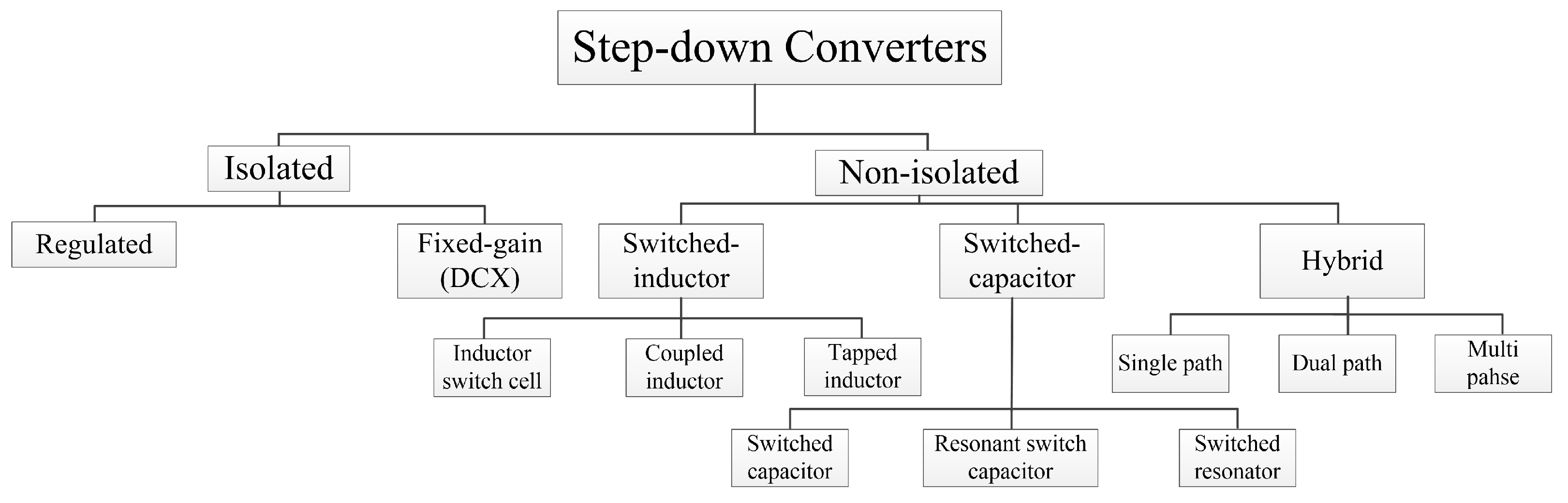
2. Voltage Step-Down Methods

The input voltage of a converter can be step-down, using either isolated or non-isolated converters, as shown in Figure 1. The isolated converters are based on the high-frequency transformers (HFT), and they can be used as either DC transformers (DCX) or voltage regulators. The non-isolated converters are realised, using either a switched inductor, a switched capacitor, or combining them. Inductors and capacitors are used to transfer energy in the first two converter classes, and both are employed in the latter case, known as hybrid converters. Moreover, converters that belong to these classes can be further divided into sub-classes, by considering their realisation and behaviour, as in Figure 1. Converters of these classes can be employed as a single unit or in combination, to meet the specifications. Auxiliary circuit units, such as active and passive voltage clamp circuits, can be integrated into these circuits. Although they shape the switching trajectory of the semiconductor devices, they do not help acquire additional voltage gain. Therefore, they are not taken into consideration, when classifying the converters.

3. Switched-Inductor Converters

An inductor is switched between the source and the load, to transfer power while stepping down the voltage. There is a single magnetic element in the buck and quasi-resonant buck converters, to transfer power. The other two converter classes, called tapped- and coupled-inductor converters, have complex magnetic structures, to acquire higher gains and improve converter performance, as explained in the following subsections.

3.1. Buck and Quasi-Resonant Buck Converter

The buck converter shown in Figure 2a is the well-known solution to step down a voltage, while regulating the output. However, it cannot be used in its pure form because of the power losses of the diode and inductive filter, in high-current applications. The diode losses are minimised, replaced with a synchronous rectifier. The interleaved operation helps minimise inductor losses [7], despite the resultant converter having a higher number of active and passive devices. The buck converter does not have very high efficiency, when providing high- to ultra-high-voltage gains, operating at extreme duty ratios. Many other converter types have been proposed, focusing on this problem, as explained in the following subsections. The buck converter is a hard-switched converter and has higher switching losses. To overcome this problem, the switching trajectory of the semiconductor devices has been modified, by integrating resonant inductors and capacitors, and the resultant units are called resonant switches [8,9]. The resonant switch depicted in Figure 2b has zero-current switching (ZCS) turn-on and -off. The resonant switch shown in Figure 2c has zero-voltage-switching (ZVS) because of the parallel capacitor. The switching frequency of quasi-resonant converters should be modulated, to vary the converter gain. A comprehensive comparison of the quasi-resonant converter types and their operation can be found in [10]. By extending the resonant switching concept, an optimal converter has been derived in [11], and it is shown in Figure 2d.

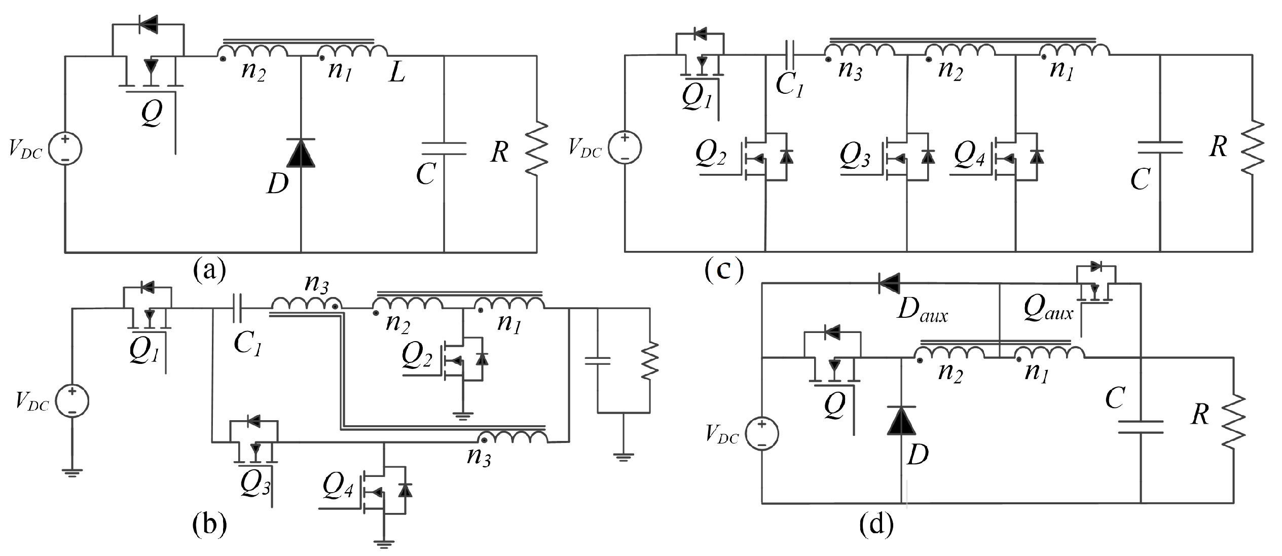
3.2. Tapped-Inductor-Based Converters

The output filter inductor of the conventional buck converter is replaced using a tapped inductor (TI), to add an extra degree of freedom to control the converter voltage gain, as shown in Figure 3a [12]. The TI buck converter configuration has been rearranged, to simplify the gate driver requirement, as explained in [13], and the resultant converter is a coupled inductor converter, having the same voltage-conversion gain. However, the output current ripple is significant, and, hence, the output-filter-capacitor requirement is large. Moreover, there is a discontinuous inductor current, under certain loading conditions. As a result, there are right-half-plane zeros. Thus, it gives rise to complex controller design.
To overcome these problems, a multi-phase buck converter, shown in Figure 3b, has been proposed [14]. Different voltage gains can be obtained, by changing the tapping point of the inductor, as discussed in [15,16,17]. The voltage gain of diode-tapped converters can be further increased, by adding a tertiary winding to the inductor and a series capacitor, as shown in Figure 3c [18]. The converter is a derivative of the series capacitor TI converter, proposed in [19]. The output current ripple of these converters can be minimised, using an additional phase, while using the same magnetic core to realise the inductors, as in [14]. An auxiliary circuit comprising of an additional switch and a diode, to change the equivalent inductance, has been added, as shown in Figure 3d, to minimise the steady-state inductor current ripple, and the converter transient response [20]. Moreover, bi-directional power transfer capability has been introduced into the series capacitor tapped inductor converter in [21], with the help of an additional switch and a clamping capacitor.

3.3. Multi-Phase and Coupled-Inductor Converters

There is a magnetic energy transfer element at the output of a step-down converter. It eliminates the pulsating nature of the output current because of the current source property. However, there is a ripple on top of the average output current, and it should be minimised to reduce the output filter capacitor requirement. The ripple magnitude can be reduced using multi-phase operation, as in [22]. To this end, the output current is interleaved by 360 n ; where n is the number of interleaved phases. The additional phases add semiconductor and passive devices that cause an extra burden on the converter optimisation, especially efficiency. The active switches switch the input voltage, and, hence, they should have high blocking voltage with higher on resistance. It gives rise to higher conduction losses. The duty ratio of these converters has been extended, by tapping the inductor, as demonstrated in [23]. However, leakage energy of the magnetic elements degrades the performance of these converters, and that problem can be circumvented to a certain extend, by coupling the magnetic elements. Coupled inductors reduce the magnetic volume of a power converter, besides the performance improvements in the steady-state and transient conditions of a voltage regulator [7]. Apart from that, the winding turns ratio can be adjusted, to get the required voltage gain, by scaling the duty ratio [24]. The performance of these coupled inductor converters can be improved, using soft-switching techniques. To this end, resonant tanks can be integrated, as in [25]. It helps to shape not only the switching trajectory of active semiconductor devices but also the voltage gain. However, either solution is not a viable option to get high- to ultra-high step-down ratios. Coupled inductors can be integrated into the conventional buck converter, to obtain higher gain, as in [26]. The energy stored in the leakage inductance has been recycled, using a clamp circuit.

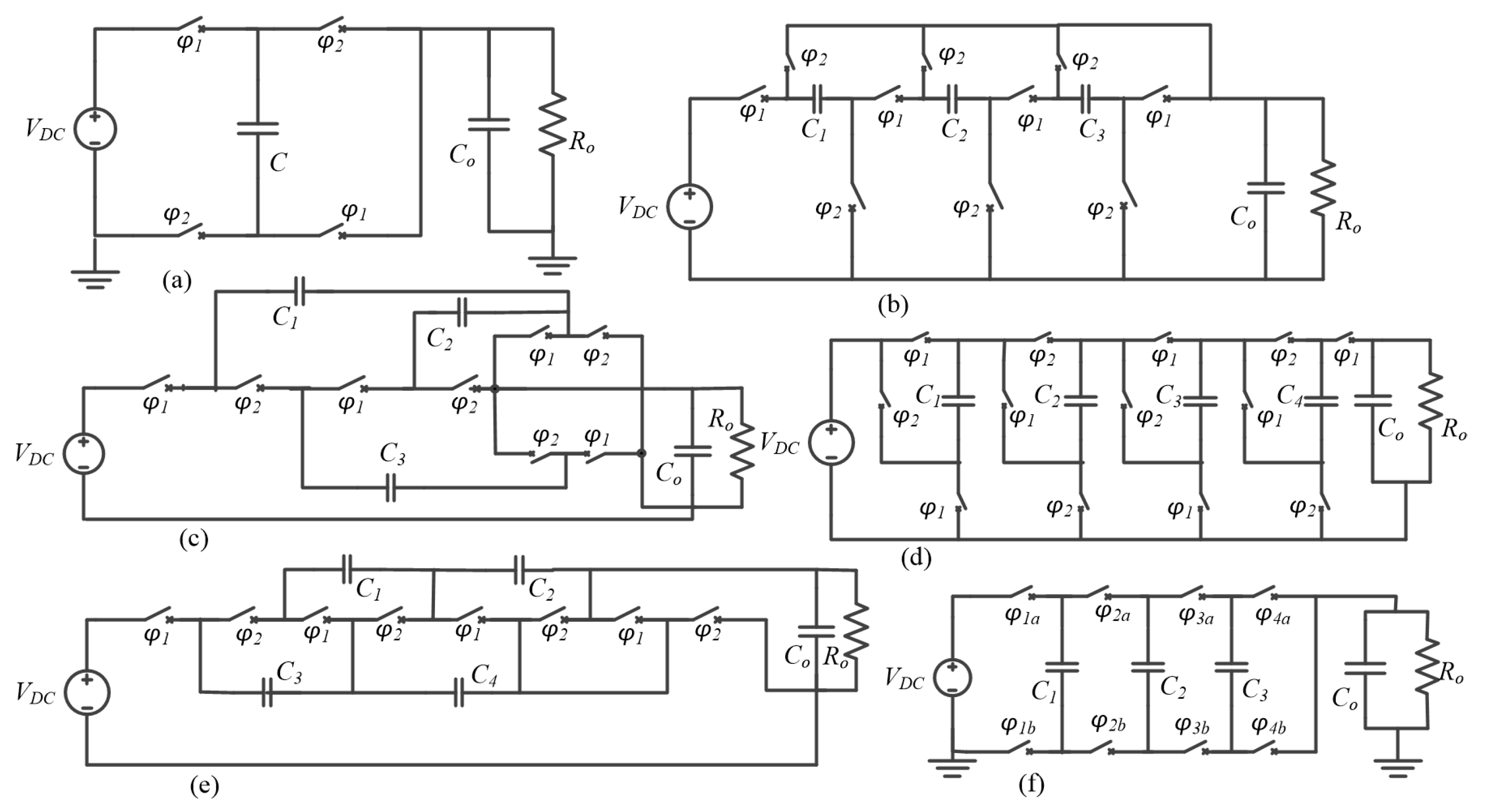
4. Switched-Capacitor Converters

Converters of this class use capacitors as the energy transfer element. It helps increase the power density of converters. However, the charge distribution through a capacitor is exponential, and, hence, there are some disadvantages in the resultant converters. To overcome this problem, the original converters belonging to this category have been modified, by integrating an element having current source properties. It could be a converter or an inductor. The resultant converters are called hybrid, switched resonator, and resonant switched capacitor converters. More details about these converters are provided in the following subsections.

4.1. Pure Switched-Capacitor Converters

Converters based on a capacitor-switching network, to transfer power, have been proposed, to increase the power density, by eliminating the magnetic elements [27]. The resultant converter is called a switched capacitor or charge-pump-type converter. There are many capacitor-switching networks, known as a 2-to-1 converter, shown in Figure 4a; a series-parallel (4-to-1) converter, shown in Figure 4b; a Dickson (4-to-1) converter, shown in Figure 4c; a Fibonacci (5-to-1) converter, shown in Figure 4d; a ladder (4-to-1) converter, shown in Figure 4e; and a flying-capacitor multilevel (4-to-1) converter, shown in Figure 4f. They have structure-dependent fixed voltage conversion ratios, along with other performance limits, discussed in [28,29]. Therefore, they can be cascaded to get higher gains. Moreover, they have high input and output current ripples as well as higher electromagnetic noises. A capacitor voltage divider, connected at the input [30], as well as converter paralleling [31] and interleaved output [32], are the strategies proposed to mitigate this problem. The output voltage of these converters has been controlled, by varying the switching frequency, considering its relationship with the equivalent output impedance [33]. However, it is not an ideal solution, when considering the realisation of the electromagnetic interference avoidance filters. As a solution, control strategies based on duty ratio modulation [34,35,36] have been proposed, to regulate the output voltage in a limited range. Moreover, there is relatively low efficiency in these converters, with the exponential charge distribution among capacitors. The split-phase control method has been proposed in [37], ensuring each capacitor has an equal voltage at the transition, using more of the buffer stage.

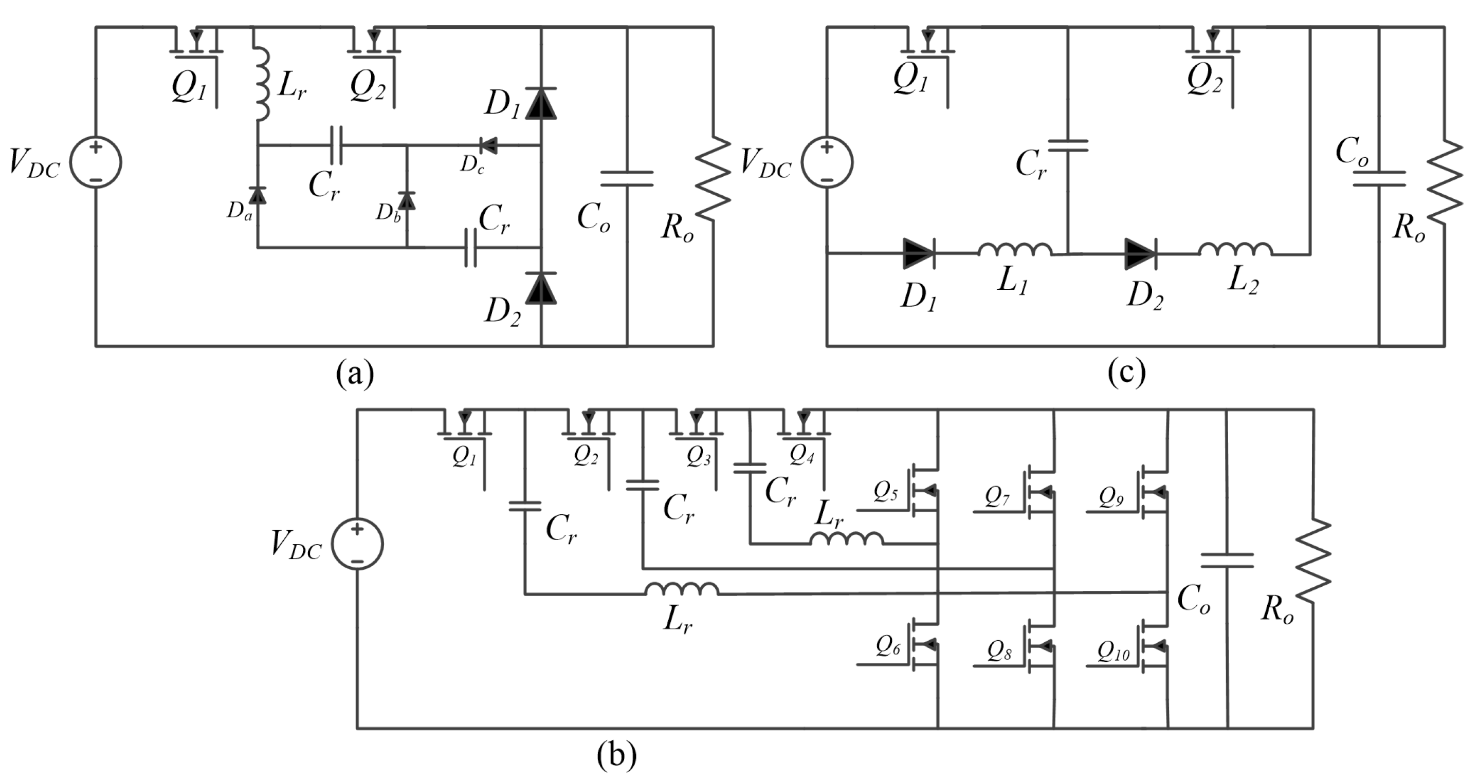
4.2. Resonant Switched-Capacitor Converters

Another solution, to control charge-distribution loss, is placing an inductor in series with the energy-transfer capacitor, as shown in Figure 5a. The resultant converter is called a resonant switched-capacitor (ReSC) converter [38]. The resonant half-wave operation gives rise to zero-current-switching (ZCS), at the turn-on and -off instance. An inductor has been integrated into the flying capacitor multi-level converter, in [39]. These converters can be cascaded, to get higher gain and increase the power density, as illustrated in [40]. The inductor can be realised as a single element, as shown in Figure 5b, or distributed elements, as illustrated in Figure 5c [41]. The output impedance and losses depend on the converter topology and the switching frequency. The dead-time control-based voltage regulation method has been proposed, using parametric analysis of the converter, considering the component non-idealities in [36,42]. The capacitor charging time has been controlled, while having a constant discharging time, to control the output voltage in [43]. Pulse density has been modulated in [44], to control the output voltage. However, these control methods help regulate the output voltage, within a limited range. The dual-phase version of the conventional resonant switched-capacitor converters has been proposed in [45], to obtain reduced output voltage ripple and high power density.

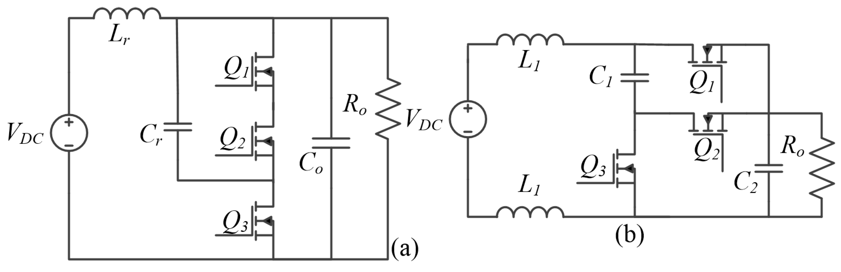
4.3. Switched-Resonator Converter

A switched-capacitor network can be integrated with a distributed inductor, to give rise to another converter class, having voltage step-down capability. It is called a switched-resonator converter (SwRC). The converter depicted in Figure 6a [46] has two resonant networks, during the two sub-intervals of the operation. Another converter class, called a switched-tank converter (STC), has been proposed, based on the same fundamental concept in [47,48]. Figure 6b shows a converter with a different resonant-tank configuration during the two sub-intervals of the operation. The resonant inductor currents complete one-half cycle, during their conduction period, and, hence, the associated switches have ZCS turn-on and -off. Converters have fixed voltage gain, which can be obtained by considering the charge balance of the capacitor. It is one limitation of both SC and ReSC converters, and the above two converters have the same problem. As a solution, it is suggested to employ multiple resonant tanks to process power, while using at least one inductor in multiple operating modes. The inductor connected to the load shown in Figure 6c is operated in both linear and resonant modes to regulate the output voltage in a wider range in [49]. The closed-form solution for the converter gain in [50] shows that the switched resonator converters can be controlled by modulating either duty ratio, as conventional DC-DC converters or switching frequency. A switched-resonator converter having a wide voltage gain range has been proposed in [51,52]. The duty ratio range to regulate the output voltage can be adjusted by varying the ratio between the inductors.

5. Hybrid Converters

Inductors are integrated into the switched capacitor converters, to control the charge distribution characteristics of the switched-capacitor converters. The resultant converter is in the resonant mode, when the switching frequency ( f s ) equals the resonant frequency ( f r ) of the LC circuit. The converter is considered an ReSC converter, in this case. The converter goes into multi-mode, i.e., the inductor has both resonant and linear operation, when the f s is higher than the f r , as explained in Section 4.3. Both ReSC and SwRC have a similar behaviour. When the f s is much greater than the f r , inductors only operate in the linear mode, and the resultant converter is called a hybrid converter. Both the inductor and capacitor are involved in the power transfer, from the input to the output, in the hybrid converters. Converters of this class can be classified as single-path, dual-path and multi-phase converters, by considering the number of energy-transfer paths connected to the load. Furthermore, there are two other converter types, called series-capacitor buck and three-level buck converters. More details about these converter classes are presented in the following sections.

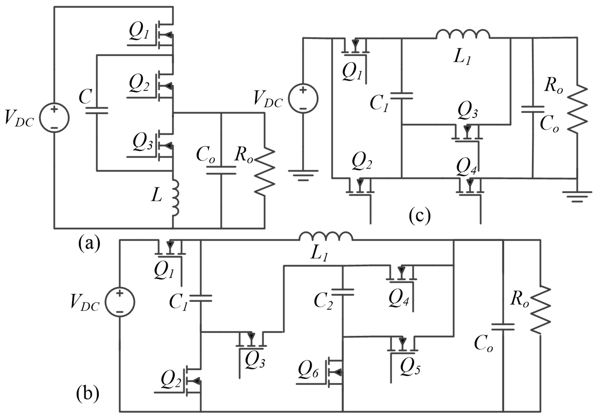
5.1. Extended or Series-Capacitor Buck Converters

A higher conversion ratio is a concern, when step-down converters are used as voltage regulators. This aim is achieved by introducing a capacitor into the two-phase buck converter, as shown in Figure 7a [53], and the three-phase converter, as shown in [54]. The added capacitor scales down the input voltage, to reduce device voltage stresses and output capacitor requirements, by reducing the current ripple magnitude. The input voltage is shared among the number of phases, and it decides the duty-ratio range, to regulate the output voltage [55,56]. The series-capacitor converter has a linear gain within a limited duty-ratio range, and beyond that, there is a quadratic relationship. A switching-control strategy for the two-phase series capacitor converter has been proposed in [57], to obtain a linear gain in the full range. Moreover, the voltage-gain range of the two-phase converter can be further extended, with help of an additional capacitor, as shown in Figure 7b [58]. A series-capacitor-based front has been introduced in [59], to reduce the inductor-switching-node voltage. The flying capacitor of all the above converters is passively stabilised, besides the balanced current sharing among inductors, due to capacitor-charge balance. However, all the switches should block full-input voltage at the start up, since the series capacitors are not charged. The introduced modification to the series-capacitor converter front-end, shown in Figure 7c [60], charges two capacitors in a series at the start up, to eliminate the above drawback. A similar strategy has been employed to divide the input voltage to acquire a higher gain for the converter, proposed in [61]. It helps to reduce the voltage stresses and losses in the devices. Moreover, the extended buck converter and its derivatives have a hard-switching operation. A resonant tank is placed in series with the energy-transferring capacitor, to realise the soft-switching operation, as shown in Figure 7a [62].
The load transients response can be further improved, by coupling the output filter into a single magnetic structure, as explained in [63,64], compared to the conventional two-inductor realization. Furthermore, a series capacitor has been employed in the tapped-inductor buck converter, as a part of the resonant circuit formed by an additional inductor, in series with the extra switch [65]. The switch helps transfer the energy stored in the tapped inductor to the output, through the formed resonant circuit. The same approach has been incorporated in the tapped-inductor converter, shown in Figure 7d [66], to recycle the energy stored in the leakage inductance. Both converters have higher voltage-step-down gain, and it is a function of the tapped-inductor turns ratio and leakage inductance. A variant of this converter has been derived, by paralleling two converters and ground referencing the energy circulation switch [67], besides modifying the front end of the resulting converter, similar to the series capacitor converter in [68].

5.2. Three-Level Buck Converter

Series-connected switching devices and flying-capacitor-based converters have been proposed, to reduce voltage stresses on the semiconductor devices in [69]. This strategy has been proposed for the inverter application, intially, and it is extended for the DC–DC converters in [70]. These converters belong to the hybrid converter family because a capacitor and an inductor are used to deliver the power, as shown in Figure 8a. The converter topology can be directly employed to step down high input voltage, with a modified switching sequence that effectively doubles the switching frequency. It reduces the switching ripple and size of the filter elements, as well as increases the converter’s open-loop bandwidth and the efficiency, as demonstrated in [71]. A different realization of the three-level buck converter has been proposed, as shown in Figure 8b [72], with similar properties. Moreover, they are paralleled, to reduce the device current stresses and output-current ripple to minimise the output-filtering requirements [73]. The flying capacitor should maintain the desired voltage at the start-up and steady-state conditions, to have the required gain and reduce device stresses. To this end, different control strategies have been proposed. Among them, a valley-current-control-based method is applied in [74]. Moreover, a transient-control strategy for a modified three-level converter has been proposed in [75]. Additional active and uncontrolled semiconductor devices are added into the proposed converter, when active only during load-transient conditions. Moreover, some converters belonging to this class can be used as bi-directional converters, and one such converter has been reported in [76]. It operates in the buck-mode, when transferring energy from the high-to-low voltage direction.

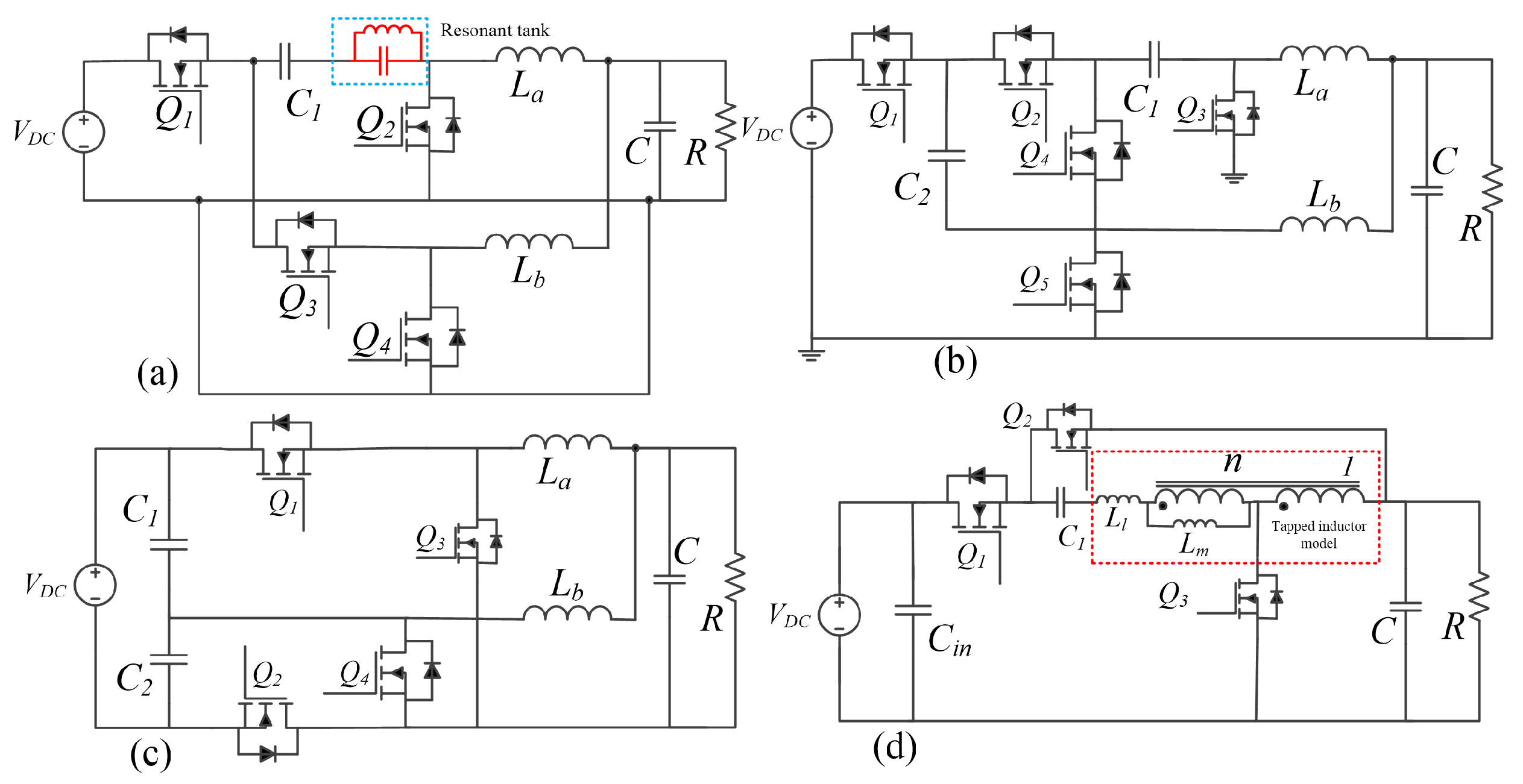
5.3. Single-Path Converters

There is a single energy-transfer path between the energy-transfer element, source and load, during the different sub-intervals of operations in this converter class. Such a hybrid converter can be realised, using the switched-inductor and switched-capacitor cells proposed in [77]. They are embedded with the existing non-isolated DC–DC converters, to get steep voltage gains. A single-path hybrid step-down converter has been realised, by dividing the input DC-link, using a switched capacitor network, and connecting buck converters across the capacitors. The buck converters are controlled as interleaved units in [78]. This approach is more useful when designing the power stage of portable systems. A single-path hybrid converter with an inductor connected to the input port has been proposed in [79,80], as shown in Figure 9a,b. The converter has higher efficiency, since the equivalent series resistance of the inductor does not make a significant contribution to the total converter power loss. An analytical method, to compare passive component volumes of switched-capacitor hybrid converters, has been proposed in [81].

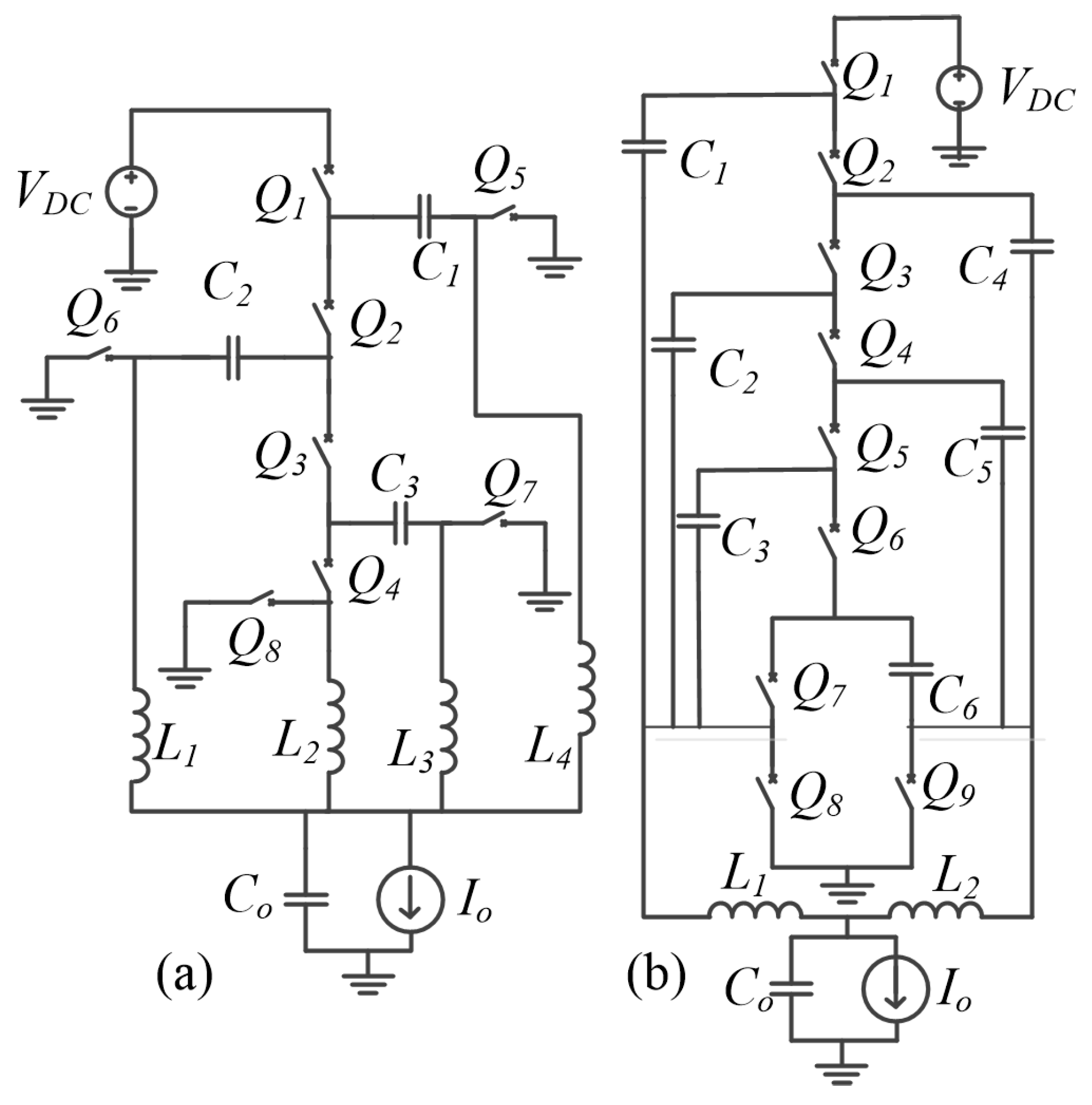
5.4. Dual-Path Converters

The power losses, due to the parasitic resistance of the inductors at the output stage of the high-current and low-voltage single-path hybrid converter, is a bottleneck behind the efficiency improvement. The dual-path converters reduce these losses, by sharing the output current among different branches connected to the load. The basic concept of dual-path converters has been presented in [82], along with a novel converter that belongs to the converter family, as shown in Figure 10a. Other converters belonging to this family have been presented in [83,84]. Different from the above case, the converter shown in Figure 10b has dual paths, during two sub-intervals of the operation [85]. Moreover, a converter having a dual path, during the energy-storing state of the hybrid converter, is proposed in [86], as depicted in Figure 10c. A dual-path hybrid converter, based on the series capacitor, is proposed in [87]. The converter has been realised, by paralleling the series capacitor converter with the dual-path hybrid converter.

5.5. Multi-Phase Converters

In this converter class, there are multiple inductors connected to the load, to share the output current and switched capacitor network, to step down the input voltage. The capacitors are charged and discharged, while keeping the inductors in their loops. As a result, there are reduced losses and electromagnetic noises, with the absence of exponential-charge distribution in the converter. As a result, the output-voltage gain becomes a function of the duty ratio and the ratio of the pure flying-capacitor-converter gain. A multi-path converter integrating an inductor to each energy transferring capacitor is proposed in [88] as shown in Figure 11a. Dual-path converters shown in Figure 11b, based on a similar concept have been proposed in [89,90,91]. The inductors of these converters are operated in interleaved mode, and they are in series with capacitors when they are charging and discharging. The voltage gain of these converters can be regulated as in conventional DC-DC converters modulating the pulse width of the control signals.

6. Multi-Stage Converters

Another strategy to gain a high step-down ratio is using multi-stage converters. In most cases, two-stage converters have been used, considering the efficiency and power density. The first stage can be realised, using an unregulated converter to maintain efficiency. It can be either an isolated LLC converter, as proposed in [92], or a non-isolated converter, as proposed in [64]. In [64], the current stresses on the devices and, hence, the losses have been minimised, using parallel converters. The voltage stresses on the first-stage converter have been reduced, using input-series converters in [93,94] and using three-level converters in [95]. The series input can be realised, using either stacked converters or the series winding of an isolation transformer. The secondary stage of low-output voltage and high-current applications has high-current stresses on the semiconductor devices and losses in the magnetic devices. To minimise the volume of the magnetic devices, parallel converters have been employed with integrated magnetic structures [93,95]. The two stages can be connected via a strong DC link or using a virtual link. The DC-bus capacitance is a bottleneck, when increasing the power density of the multi-stage converters. To minimise the DC-link capacitance requirement, converters having virtual DC linked, as shown in Figure 12, have been proposed. The converter has a topology-dependent switching-control strategy [96,97].

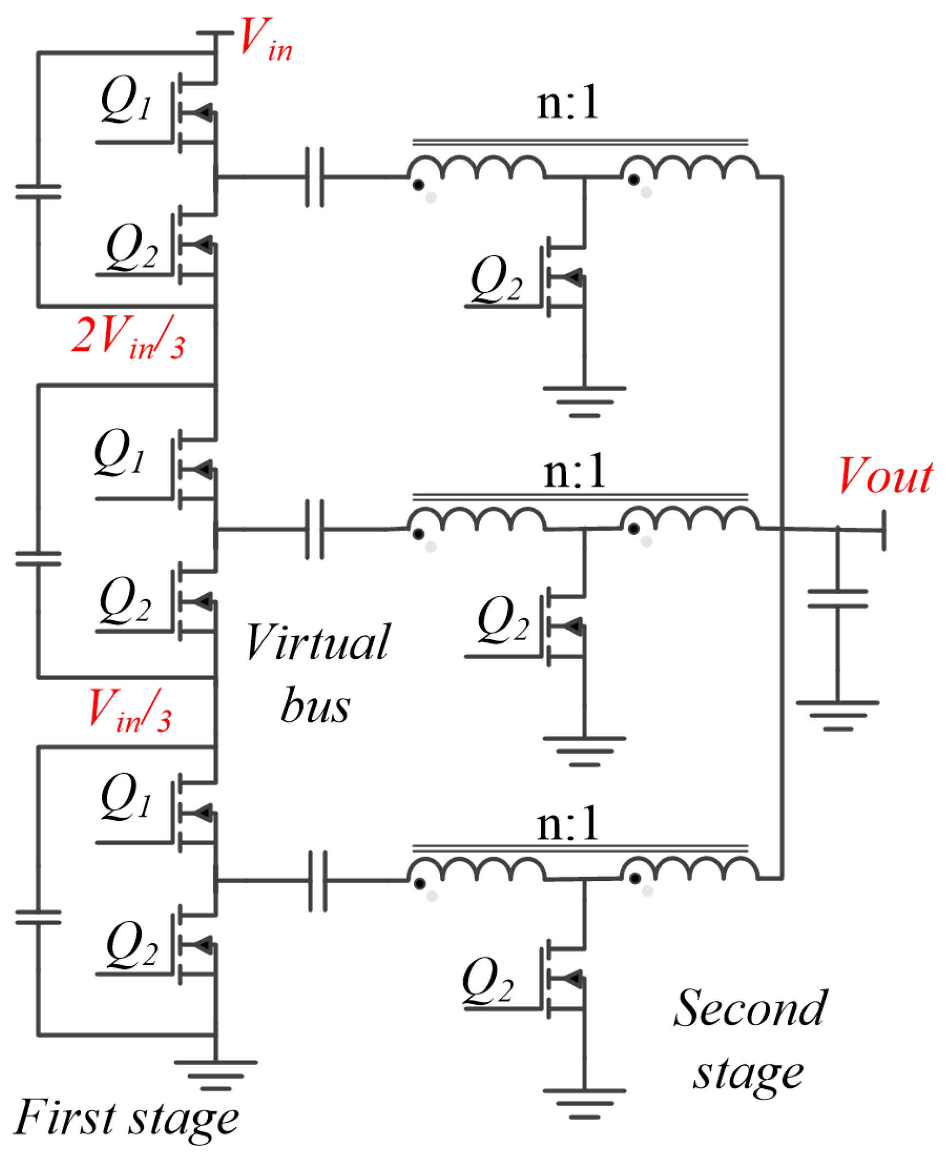
7. High-Frequency Transformer-Based Converters

High-frequency transformer-based topologies help step down input voltage, while providing electrical isolation between the source and load. These converters can be a part of multi-stage converters, as discussed in the above section, or single-stage converters. In the single-stage converters, they might be used in different configurations, to obtain the required gain. Phase-shifted full-bridge (PSFB) has been used as the building block of the series-input parallel-output converter, presented in [98]. The dual-active bridge (DAB) is the basic building block in this converter, and its HFT can be realised using integrated structures, as in [99], to increase the power density. The input-side switches of the converter, presented in [99], experience high stresses. This drawback can be eliminated, using the stacked-DAB configuration, proposed in [100], since the input voltage is shared among series-connected switches. DAB, with a dual phase-shift-based control strategy, has been used in pulse-power application in [101]. Different modulation and control strategies employed with the DAB converters have been discussed in [102]. LLC-resonant converters are widely used as unregulated converters, due to their optimal performance at the selected switching frequency. They can be realised, using conventional and matrix transformers, as discussed in [4]. Furthermore, to enhance the power-processing efficiency, partial power-processing architecture and suitable converter topologies have been proposed in [103]. The unregulated power path of the converter, presented in [103], has been realised using an LLC converter, based on the matrix transformer. A transformer for an LLC converter, having a quarter secondary winding, has been proposed in [104], to reduce DC resistance and, hence, improve efficiency.

8. Comparison between the Converter Classes and Outlook

In the above subsections, more details about the different converter subclasses have been discussed, and outcomes are summarised in Table 1. Furthermore, a quantitative comparison between the converters is provided in Table 2. The analysis shows that isolated converters, based on an HFT, are ideal for high-voltage and high-power applications. The passive voltage gain of HFT is crucial, when the power supply needs to be realised as a single unit, without an intermediate bus. In those applications, input series and parallel-output configurations give optimal performance, when considering the stresses on the semiconductor devices and losses in the magnetic devices. The series input can be realised, by using either multiple stacked cells or series-transformer windings. Multiple converter cells can be interleaved, to share the output current in low-voltage applications. The converter power density can be further increased, by using integrated magnetic structures and virtual intermediate links, supported by the converter-control strategies. To this end, hybrid converters, based on the multiple output phases, could be another suitable candidate. On the other hand, the power supply can be realised, using cascaded converters connected by an intermediate bus. The system front end might be based on a converter having known gain, i.e., an LLC converter operating at a fixed point. It guarantees the ZVS operation, under different loading conditions. The converters based on switched-tank topologies can be employed, by considering their load-independent soft-switching characteristics. The load-connected regulated stage can be realised, using a converter belonging to the switched capacitor converter family, by considering their power density. However, the converters based on pure SC converters might not be ideal candidates, due to low efficiency, topology-specific voltage gain, and discrete voltage-conversion ratios. This drawback can be overcome, using derivatives of that converter class, such as ReSC and SwRC converters. Among them, SwRCs have the most desirable features, for use in low-power applications.
Apart from the converter topologies, power-semiconductor and magnetic-device realization play a crucial role in the efficiency and power density improvement. Semiconductor devices, based on the wide-band-gap materials, such as GaN and SiC, help minimise losses in the hard-switched topologies operating at high- to very-high frequencies, due to their superior switching properties. Moreover, they have high blocking voltage and low on-resistance, even at higher temperatures, compared to the Si devices [105]. The third factor behind the performance improvement is magnetic-device realization. It has been shown that many small inductors in series or parallel combinations are not a viable solution, due to the volume and total losses [106]. Hence, the integrated magnetics sharing the same core, for many conductors, has become one of the solutions in high-power applications. On the other hand, in low-power applications, the thin-film-on-die realization has gained the lead, with the advancement of the materials. These magnetic structures can be realised as coupled inductors, to cancel DC flux to avoid saturation [107], using nano-granular materials [108] and having radial anisotropy [106]. Nano-granular materials help increase resistivity, to reduce losses. The radial anisotropy helps reduce the excess eddy current losses because of the vias. Another challenge behind the performance improvement in step-down converters is fulfilling the capacitance requirement of the energy-transfer and filter elements. Class II multi-layer ceramic capacitors are used in SC and hybrid converter topologies, considering their high-energy density, when considering the discrete capacitors. However, there are changes in capacitance and equivalent series resistance (ESR) with ageing, temperature and electric field. Thus, the performance of the SC and ReSC converters can be impacted by these effects [109]. On the other hand, thin-film technology has been employed to realise capacitors in integrated voltage regulator (IVR) applications. It reduces the ESR and equivalent series inductance, to use them in HF applications, while embedding them into the printed circuit boards.
Most of the step-down converters analyzed in this article have a hard-switching operation. There are switching losses at the turn-on and -off transitions, in the active switches and reverse-recovery losses in the diodes. These losses are proportional to the switching frequency, and it is a hurdle, when improving the efficiency of the Si-device-based converters. To minimise switching losses, resonant tanks have been integrated [110] or have realised the help of the parasitic elements of the magnetic and semiconductor devices [111]. The resultant resonant-converter experiences ZVS and ZCS, at the switching transitions. Apart from that, voltage and current stresses on the semiconductor devices play an important role, when considering the converter reliability. The switch current depends on the converter topology. The device voltage depends on both topology and the rate of change of the current. The voltage stresses can be reduced, by minimising the parasitic inductances of the printed circuit board, following good design practices. When it considers the integrated magnetic elements, the energy stored in the leakage inductance should be dissipated or recycled, to minimise the stresses on the semiconductor and passive devices. To this end, passive snubbers [112] or active clamping elements [113] can be integrated into the converter.

9. Topology Derivation

Synthesising the non-isolated step-down converter topology, when the voltage gain polynomial (VGP) is given along the input and output current ripple as well as the desired duty ratio range, is another challenging task [85]. The converter synthesis, starting from the VGP, is called an inverse problem. To this end, there are several approaches, known as the connection matrix method [114], along with the design rules [115], state-space model-based [116], flux-balance method [117] and low-entropy-equations-based method [118,119,120,121]. Connection-matrix-based methods and their derivatives give redundant, non-realizable and degenerative solutions, at the end of the synthesis process, since they are based on the high-entropy equations that contain more unknowns than equations. The state-space-based methods user should have experience and intuition when synthesising the converter. Moreover, they have limited usability, when synthesising converters containing capacitor-only loops. Therefore, the design-oriented low-entropy-based method helps synthesise converters, belonging to the non-isolated branch of Figure 1.
The operation of the synthesised converters is analysed, by considering the voltage-second balance of the energy transfer inductor, using the method explained in [122]. A converter could be in either continuous-conduction, boundary or discontinuous-conduction modes, depending on the loading condition. Several basic step-down converter topologies in different operation modes have been analyzed in [122]. However, the converters are synthesised, assuming that the converter is in the continuous conduction mode.

10. Converter Control

DC–DC converters act as either a voltage regulator or a DC transformer (DCX), when it is connected between a source and a load. The converter should maintain a constant voltage across the load terminal, despite variations in the source voltage and the load. However, intermediate-link DC–DC converters act as a DCX. They are based on the open-loop controllers and maintain a constant output voltage, without regulating it. Voltage regulators have a closed loop, to track the desired output. The converter’s transient response has a significant impact on both the converter topology and the controller realisation method. The controllers are realised by either sensing output voltage, called voltage-model controller (VMC) [123], or measuring the inductor current, called current-model controller (CMC) [124]. They are known as feedback control strategies because the output is compared against a reference signal in the controller model. Disturbances are predicted in the feed-forward controller, to inject them into the controller loop to minimise their impact. There are two other frequently used controller-implementation methods, known as observer-based feedback control and predictive control. The compensator of the feedback loop is implemented using linear approaches, called proportional (P), proportional-integral (PI) and proportional-integral-derivative (PID) controllers. The integral controller is known as a Type I compensator. When it is cascaded with a phase-lead network, it is called a Type II compensator, and when there are two cascaded phase-lead networks, it is called a Type III compensator [125].
The control signals of these controllers can be implemented using fixed-frequency pulse-width-modulated (PWM) control signals. The implementation can be based on either analog circuits (operational/transcendence amplifiers) or a digital controller, such as a microcontroller and a digital signals processor. The sampling frequency of the analog-to-digital converters (ADC) influences the controller performance, compared to the analog counterpart. Moreover, active switch control signals might have variable switching frequencies. In one implementation, the switch is turned off for a fixed time interval, and on time is modulated [126]. This strategy is called constant off-time modulation. On the contrary, the on time can be modulated, and the resultant modulation method is called the constant-on-time modulation [127]. Both approaches do not have stability issues, but they are based on the variable frequency operation. Apart from that, there is a control strategy called hysteresis control. It determines the switching instant, rather than the pulse width, constraining the inductor current within a band. Therefore, it can not be considered a PWM strategy [128]. Besides the PWM strategies, phase-shift modulation (PSM) is used to control the power flow, especially in dual-bridge-based step-down converters. The phase angle between the terminal voltage of the two bridges is modulated, to determine the power-flow direction and magnitude. It gives rise to higher RMS transformer current, under the light-load conditions. The phase shift modulation between control signals of the two legs of a single bridge increases the degree of freedom. There is a comprehensive review of the PSM-based control strategies, used in the bridge converters, in [102]. A comprehensive analysis of DC–DC power-converter-controller design methods can be found in [129].

11. Conclusions

In this article, a comprehensive overview of the existing step-down converter architectures and topologies is presented. The analysis shows that these converters can be broadly categorised into two groups, considering the transformer isolation. The transformer-isolated converters have either fixed or regulated output. The non-isolated converters are based on the switched-inductor, switched-capacitor and hybrid converters. They have different sub-classes that can be identified, based on their topology and operation. They are ideal candidates to realise the point-of-load converters in low-power applications. Among them, hybrid converters gain attention because of their desirable features. On the other hand, the multi-stage converters are helpful in the high-power applications.

Author Contributions

Writing review and editing, D.N.; supervision and article review, Y.L. All authors have read and agreed to the published version of the manuscript.

Funding

This research was supported by the Canada First Research Excellence Fund (CFREF) - Future Energy Systems Research Initiative at the University of Alberta.

Conflicts of Interest

The authors declare no conflict of interest.

References

  1. Bindra, A. Driven by Density, Efficiency at Low Cost, Power Integration Reaches New Heights. IEEE Power Electron. Mag. 2022, 9, 14–19. [Google Scholar] [CrossRef]
  2. Giasson, A.; Dokopoulos, S. Rethinking the Power Delivery Networks of Mobile Robots. IEEE Power Electron. Mag. 2020, 7, 12–18. [Google Scholar] [CrossRef]
  3. Krein, P.T. Data Center Challenges and Their Power Electronics. CPSS Trans. Power Electron. Appl. 2017, 2, 39–46. [Google Scholar] [CrossRef]
  4. Fei, C.; Lee, F.C.; Li, Q. High-Efficiency High-Power-Density LLC Converter with an Integrated Planar Matrix Transformer for High-Output Current Applications. IEEE Trans. Ind. Electron. 2017, 64, 9072–9082. [Google Scholar] [CrossRef]
  5. Xue, F.; Yu, R.; Huang, A. A Family of Ultrahigh Efficiency Fractional Dc-Dc Topologies for High Power Energy Storage Device. IEEE JESTPE 2021, 9, 1420–1427. [Google Scholar] [CrossRef]
  6. Chen, L.; Wu, H.; Xu, P.; Hu, H.; Wan, C. A High Step-down Non-Isolated Bus Converter with Partial Power Conversion Based on Synchronous LLC Resonant Converter. In Proceedings of the IEEE APEC, Charlotte, NC, USA, 15–19 March 2015; pp. 1950–1955. [Google Scholar]
  7. Wong, P.L.; Xu, P.; Yang, B.; Lee, F.C. Performance Improvements of Interleaving VRMs with Coupling Inductors. IEEE Trans. Power Electron. 2001, 16, 499–507. [Google Scholar] [CrossRef]
  8. Liu, K.; Lee, F.C. Resonant Switches—A Unified Approach to Improve Performances of Switching Converters. In Proceedings of the IEEE INTELEC, New Orleans, LA, USA, 4–7 November 1984. [Google Scholar]
  9. Lee, F.C. High-Frequency Quasi-Resonant Converter Technologies. IEEE Proc. 1988, 76, 377–390. [Google Scholar] [CrossRef]
  10. Jovanovik, M.M. Merits and Limitations of Resonant and Soft-Switched Converters. In Proceedings of the IEEE INTELEC, Washington, DC, USA, 4–8 October 1992; pp. 51–58. [Google Scholar]
  11. Divakar, B.P.; Sutanto, D. Optimum Buck Converter with a Single Switch. IEEE Trans. Power Electron. 1999, 14, 636–642. [Google Scholar] [CrossRef]
  12. Park, J.H.; Cho, B.H. The Zero Voltage Switching (ZVS) Critical Conduction Mode (CRM) Buck Converter with Tapped-Inductor. IEEE Trans. Power Electron. 2005, 20, 762–774. [Google Scholar] [CrossRef]
  13. Yao, K.; Ye, M.; Xu, M.; Lee, F.C. Tapped-Inductor Buck Converter for High-Step-Down. IEEE Trans. Power Electron. 2005, 20, 775–780. [Google Scholar] [CrossRef]
  14. Nishijima, K.; Ishida, D.; Harada, K.; Nabeshima, T.; Sato, T.; Nakano, T. A Novel Two-Phase Buck Converter with Two Cores and Four Windings. In Proceedings of the IEEE INTELEC, Rome, Italy, 30 September–4 October 2007; pp. 861–866. [Google Scholar]
  15. Grant, D.A.; Darroman, Y.; Suter, J. Synthesis of Tapped-Inductor Switched-Mode Converters. IEEE Trans. Power Electron. 2007, 22, 1964–1969. [Google Scholar] [CrossRef]
  16. Williams, B.W. Unified Synthesis of Tapped-Inductor DC-to-DC Converters. IEEE Trans. Power Electron. 2014, 29, 5370–5383. [Google Scholar] [CrossRef]
  17. Abramovitz, A.; Yao, J.; Smedley, K. Unified Modeling of PWM Converters with Regular or Tapped Inductors Using TIS-SFG Approach. IEEE Trans. Power Electron. 2016, 31, 1702–1716. [Google Scholar] [CrossRef]
  18. Yau, Y.T.; Jiang, W.Z.; Hwu, K.I. Ultrahigh Step-down Converter with Wide Input Voltage Range Based on Topology Exchange. IEEE Trans. Power Electron. 2017, 32, 5341–5364. [Google Scholar] [CrossRef]
  19. Nishijima, K.; Sato, T.; Nabeshima, T. A Novel Tapped-Inductor Buck Converter for Home DC Power Supply Sys Stem. In Proceedings of the IEEE ICRERA, Nagasaki, Japan, 11–14 November 2012; pp. 1–8. [Google Scholar]
  20. Gu, Y.; Zhang, D. Voltage Regulator Buck Converter with a Tapped Inductor for Fast Transient Response Application. IEEE Trans. Power Electron. 2014, 29, 6249–6254. [Google Scholar] [CrossRef]
  21. Yau, Y.T.; Jiang, W.Z.; Hwu, K.I. Bidirectional Operation of High Step-Down Converter. IEEE Trans. Power Electron. 2015, 30, 6829–6844. [Google Scholar] [CrossRef]
  22. Lee, I.; Cho, S.; Moon, G. Interleaved Buck Converter Having Low Switching Losses and Improved Step-Down Conversion Ratio. IEEE Trans. Power Electron. 2012, 27, 3664–3675. [Google Scholar] [CrossRef]
  23. Xu, P.; Wei, J.; Lee, F.C. Multiphase Coupled-Buck Converter - A Novel High Efficient 12 V Voltage Regulator Module. IEEE Trans. Power Electron. 2003, 18, 74–82. [Google Scholar]
  24. Yao, K.; Qiu, Y.; Xu, M.; Lee, F.C. A Novel Winding-Coupled Buck Converter for High-Frequency, High-Step-Down DC–DC Conversion. IEEE Trans. Power Electron. 2005, 20, 1017–1024. [Google Scholar] [CrossRef]
  25. Ge, T.; Miao, Z.; Liu, L. Active Cross-Commutated (ACC) Buck Converter. IEEE Trans. Ind. Electron. 2022, 69, 2577–2587. [Google Scholar] [CrossRef]
  26. Hajiheidari, M.; Farzanehfard, H.; Adib, E. High-Step-Down DC–DC Converter with Continuous Output Current Using Coupled-Inductors. IEEE Trans. Power Electron. 2019, 34, 10936–10944. [Google Scholar] [CrossRef]
  27. Singer, Z.; Emanuel, A.; Erlicki, M.S. Power Regulation by Means of a Switched Capacitor. Proc. IEE 1972, 119, 149–152. [Google Scholar] [CrossRef]
  28. Makowski, M.S.; MaksimoviC, D. Performance Limits of Switched-Capacitor DC-DC Converters. In Proceedings of the IEEE PESC, Atlanta, GA, USA, 18–22 June 1995; pp. 1215–1221. [Google Scholar]
  29. Mahnashi, Y.; Peng, F.Z. Generalization of the Fundamental Limit Theory in a Switched-Capacitor Converter. IEEE Trans Power Electron. 2017, 32, 6673–6676. [Google Scholar] [CrossRef]
  30. Umeno, T.; Takahashi, K.; Oota, I.; Ueno, F.; Inoue, T. New Switched-Capacitor DC-DC Converter with Low Input Current Ripple and Its Hybridization. In Proceedings of the IEEE Midwest Symposium on Circuits and Systems, Calgary, AB, Canada, 12–14 August 1990; pp. 1091–1094. [Google Scholar]
  31. Chung, H.S.-H.; Hui, S.Y.R.; Tang, S.C.; Wu, A. On the Use of Current Control Scheme for Switched-Capacitor DC/DC Converters. IEEE Trans. Ind. Electron. 2000, 47, 238–244. [Google Scholar] [CrossRef]
  32. Han, J.; von Jouanne, A.; Temes, G.C. A New Approach to Reducing Output Ripple in Switched-Capacitor-Based Step-down DC-DC Converters. IEEE Trans. Power Electron. 2006, 21, 1548–1555. [Google Scholar] [CrossRef]
  33. Seeman, M.D.; Sanders, S.R. Analysis and Optimization of Switched-Capacitor DC–DC Converters. IEEE Trans. Power Electron. 2008, 23, 841–851. [Google Scholar] [CrossRef]
  34. Cheong, S.V.; Chung, S.H.; Ioinovici, A. Duty-Cycle Control Boosts DC-DC Converters. IEEE Circuits Devices Mag. 1993, 9, 36–37. [Google Scholar] [CrossRef]
  35. Cheong, S.V.; Chung, H.; Ioinovici, A. Inductorless DC-to-DC Converter with High Power Density. IEEE Trans. Ind. Electron. 1994, 41, 208–215. [Google Scholar] [CrossRef]
  36. Suetsugu, T. Novel PWM Control Method of Switched Capacitor DC-DC Converter. In Proceedings of the IEEE ISCAS, Monterey, CA, USA, 31 May–3 June 1998; Volume 6, pp. 454–457. [Google Scholar]
  37. Lei, Y.; May, R.; Pilawa-Podgurski, R. Split-Phase Control: Achieving Complete Soft-Charging Operation of a Dickson Switched-Capacitor Converter. IEEE Trans. Power Electron. 2016, 31, 770–782. [Google Scholar] [CrossRef]
  38. Cheng, K.W.E. New Generation of Switched Capacitor Converters. In Proceedings of the IEEE PESC, Fukuoka, Japan, 22 May 1998; pp. 1529–1535. [Google Scholar]
  39. Rentmeister, J.S.; Stauth, J.T. A 48V: 2V Flying Capacitor Multilevel Converter Using Current-Limit Control for Flying Capacitor Balance. In Proceedings of the IEEE APEC, Tampa, FL, USA, 26–30 March 2017. [Google Scholar]
  40. Ye, Z.; Lei, Y.; Pilawa-podgurski, R.C.N. The Cascaded Resonant Converter: A Hybrid Switched-Capacitor Topology With High Power Density and Efficiency. IEEE Trans. Power Electron. 2020, 35, 4946–4958. [Google Scholar] [CrossRef]
  41. Liu, W.C.; Ye, Z.; Pilawa-Podgurski, R.C.N. Comparative Analysis on Minimum Output Impedance of Fixed-Ratio Hybrid Switched Capacitor Converters. In Proceedings of the IEEE COMPEL, Toronto, ON, Canada, 17–20 June 2019; pp. 1–7. [Google Scholar]
  42. Lin, Y.-C.; Liaw, D.-C. Parametric Study of a Resonant Switched Capacitor DC-DC Converter. In Proceedings of the IEEE TENCON, Singapore, 19–22 August 2001; pp. 710–716. [Google Scholar]
  43. Qiu, D.; Zhang, B.; Zheng, C. Duty Ratio Control of Resonant Switched Capacitor DC-DC Converter. In Proceedings of the IEEE ICEMS, Nanjing, China, 27–29 September 2005; pp. 1138–1141. [Google Scholar]
  44. Cervera, A.; Mordechai Peretz, M. Resonant Switched-Capacitor Voltage Regulator with Ideal Transient Response. IEEE Trans. Power Electron. 2015, 30, 4943–4951. [Google Scholar] [CrossRef]
  45. Ye, Y.; Eric Cheng, K.W.; Liu, J.; Xu, C. A Family of Dual-Phase-Combined Zero-Current Switching Switched-Capacitor Converters. IEEE Trans. Power Electron. 2014, 29, 4209–4218. [Google Scholar] [CrossRef]
  46. Yeung, B.; Cheng, K.W.E.; Sutanto, D.; Ho, S.L. Zero-Current Switching Switched-Capacitor Quasiresonant Step-down Converter. IEE Proc. 2002, 149, 111–121. [Google Scholar] [CrossRef]
  47. Li, S.; Xiangli, K.; Zheng, Y.; Smedley, K.M. Analysis and Design of the Ladder Resonant Switched-Capacitor Converters for Regulated Output Voltage Applications. IEEE Trans. Ind. Electron. 2017, 64, 7769–7779. [Google Scholar] [CrossRef]
  48. Lyu, X.; Li, Y.; Ren, N.; Jiang, S.; Cao, D. A Comparative Study of Switched-Tank Converter and Cascaded Voltage Divider for 48-V Data Center Applications. IEEE JESTPE 2020, 8, 1547–1559. [Google Scholar] [CrossRef]
  49. Cuk, S. Four-Switch Step-Down Storageless Converter. U.S. Patent 8,134,351/B2, 2012. [Google Scholar]
  50. Nayanasiri, D.; Li, Y. Voltage Gain Control of a Switched-Resonator Converter Based on the 2:1 Switched-Capacitor Cell. In Proceedings of the IEEE ECCE, Vancouver, BC, Canada, 10–14 October 2021; pp. 1762–1769. [Google Scholar]
  51. Nayanasiri, D.; Gunawardena, P.; Li, Y. Multiresonant and Multimode Operation of the Switched-Resonator Converters. IEEE Trans. Power Electron. 2021, 36, 5622–5634. [Google Scholar] [CrossRef]
  52. Nayanasiri, D.; Li, Y. Pulsewidth Modulated Switched Resonator Converter Having Continuous Buck Gain. IEEE Trans. Ind. Electron. 2022, 69, 376–386. [Google Scholar] [CrossRef]
  53. Nishijima, K.; Harada, K.; Nakano, T.; Nabeshima, T.; Sato, T. Analysis of Double Step-down Two-Phase Buck Converter for VRM. In Proceedings of the IEEE INTELEC, Berlin, Germany, 18–22 September 2005; pp. 497–502. [Google Scholar]
  54. Abe, K.; Nishijima, K.; Harada, K.; Nakano, T.; Nabeshima, T.; Sato, T. A Novel Three-Phase Buck Converter with Bootstrap Driver Circuit. In Proceedings of the IEEE PESC, Orlando, FL, USA, 17–21 June 2007; Volume 1, pp. 1864–1871. [Google Scholar]
  55. Jang, Y.; Jovanović, M.M.; Panov, Y. Multi-Phase Buck Converters with Extended Duty Cycle. In Proceedings of the IEEE APEC, Dallas, TX, USA, 19–23 March 2006; pp. 38–44. [Google Scholar]
  56. Hwu, K.I.; Jiang, W.Z.; Wu, P.Y. An Expandable Four-Phase Interleaved High Step-Down Converter with Low Switch Voltage Stress and Automatic Uniform Current Sharing. IEEE Trans. Ind. Electron. 2016, 63, 6064–6072. [Google Scholar] [CrossRef]
  57. Bui, D.V.; Cha, H.; Nguyen, V.C. Asymmetrical PWM Series-Capacitor High-Conversion-Ratio DC-DC Converter. IEEE Trans. Power Electron. 2021, 36, 8628–8633. [Google Scholar] [CrossRef]
  58. Kirshenboim, O.; Peretz, M.M. High-Efficiency Nonisolated Converter with Very High Step-Down Conversion Ratio. IEEE Trans. Power Electron. 2017, 32, 3683–3690. [Google Scholar] [CrossRef]
  59. Halamicek, M.; Mcrae, T.; Prodic, A. Cross-Coupled Series-Capacitor Quadruple Step-Down Buck Converter. In Proceedings of the IEEE APEC, New Orleans, LA, USA, 15–19 March 2020; pp. 1–6. [Google Scholar]
  60. Kim, K.; Cha, H.; Park, S.; Lee, I. A Modified Series-Capacitor High Conversion Ratio DC–DC Converter Eliminating Start-Up Voltage Stress Problem. IEEE Trans. Power Electron. 2018, 33, 8–12. [Google Scholar] [CrossRef]
  61. Chuang, C.F.; Pan, C.T.; Cheng, H.C. A Novel Transformer-Less Interleaved Four-Phase Step-down DC Converter with Low Switch Voltage Stress and Automatic Uniform Current-Sharing Characteristics. IEEE Trans. Power Electron. 2016, 31, 406–417. [Google Scholar] [CrossRef]
  62. Tu, C.; Chen, R.; Ngo, K.D.T. Series-Resonator Buck Converter—Viability Demonstration. IEEE Trans. Power Electron. 2021, 36, 9693–9697. [Google Scholar] [CrossRef]
  63. Oraw, B.S.; Ayyanar, R. Voltage Regulator Optimization Using Multiwinding Coupled Inductors and Extended Duty Ratio Mechanisms. IEEE Trans. Power Electron. 2009, 24, 1494–1505. [Google Scholar] [CrossRef]
  64. Chen, Y.; Giuliano, D.M.; Chen, M. Two-Stage 48V-1V Hybrid Switched-Capacitor Point-of-Load Converter with 24V Intermediate Bus. In Proceedings of the IEEE COMPEL, Aalborg, Denmark, 9–12 November 2020; pp. 1–8. [Google Scholar]
  65. Cuk, S. Step-down Converter Having a Resonant Inductor, a Resonant Capacitor and a Hybrid Transformer. U.S. Patent 7,915,874 B1, 2011. [Google Scholar]
  66. Chen, M.; Shenoy, P.S.; Morroni, J. A Series-Capacitor Tapped Buck (SC-TaB) Converter for Regulated High Voltage Conversion Ratio Dc-Dc Applications. In Proceedings of the IEEE ECCE, Pittsburgh, PA, USA, 14–18 September 2014; pp. 3650–3657. [Google Scholar]
  67. Zhao, X.; Yeh, C.; Zhang, L.; Lai, J. A High-Frequency High-Step-down Converter with Coupled Inductor for Low Power Applications. In Proceedings of the IEEE APEC, Tampa, FL, USA, 26–30 March 2017; pp. 2436–2440. [Google Scholar]
  68. Zhang, L.; Chakraborty, S. An Interleaved Series-Capacitor Tapped Buck Converter for High Step-Down DC/DC Application. IEEE Trans. Power Electron. 2019, 34, 6565–6574. [Google Scholar] [CrossRef]
  69. Meynard, T.A.; Foch, H. Multi-Level Conversion: High Voltage Choppers and Voltage-Source Inverters. In Proceedings of the IEEE PESC, Toledo, Spain, 29 June–3 July 1992; pp. 397–403. [Google Scholar]
  70. Pinheiro, J.R.; Barbi, I. The Three-Level ZVS-PWM DC-to-DC Converter. IEEE Trans. Power 1993, 8, 486–492. [Google Scholar] [CrossRef]
  71. Yousefzadeh, V.; Alarcón, E.; Maksimović, D. Three-Level Buck Converter for Envelope Tracking Applications. IEEE Trans. Power Electron. 2006, 21, 549–552. [Google Scholar] [CrossRef]
  72. Ruan, X.; Li, B.; Chen, Q.; Tan, S.C.; Tse, C.K. Fundamental Considerations of Three-Level DC-DC Converters: Topologies, Analyses, and Control. IEEE Trans. Circuits Syst. I Regul. Pap. 2008, 55, 3733–3743. [Google Scholar] [CrossRef]
  73. Yerra, S.; Krishnamoorthy, H. Multi-Phase Three-Level Buck Converter with Current Self-Balancing for High Bandwidth Envelope Tracking Power Supply. In Proceedings of the IEEE APEC, New Orleans, LA, USA, 15–19 March 2020; pp. 1872–1877. [Google Scholar]
  74. Reusch, D.; Lee, F.C.; Xu, M. Three Level Buck Converter with Control and Soft Startup. In Proceedings of the IEEE ECCE, San Jose, CA, USA, 20–24 September 2009; Volume 2, pp. 31–35. [Google Scholar]
  75. Shi, L.; Baddipadiga, B.P.; Ferdowsi, M.; Crow, M.L. Improving the Dynamic Response of a Flying-Capacitor Three-Level Buck Converter. IEEE Trans. Power Electron. 2013, 28, 2356–2365. [Google Scholar] [CrossRef]
  76. Dusmez, S.; Hasanzadeh, A.; Khaligh, A. Comparative Analysis of Bidirectional Three-Level DC-DC Converter for Automotive Applications. IEEE Trans. Ind. Electron. 2015, 62, 3305–3315. [Google Scholar] [CrossRef]
  77. Axelrod, B.; Berkovich, Y.; Ioinovici, A. Switched-Capacitor/Switched-Inductor Structures for Getting Transformerless Hybrid DC–DC PWM Converters. IEEE Trans. Circuits Syst. 2008, 55, 687–696. [Google Scholar] [CrossRef]
  78. Radic, A.; Ahssanuzzaman, S.M.; Mahdavikhah, B.; Prodic, A. High-Power Density Hybrid Converter Topologies for Low-Power Dc-Dc SMPS. In Proceedings of the IEEE IPEC, Hiroshima, Japan, 18–21 May 2014; pp. 3582–3586. [Google Scholar]
  79. Gabian, G.; Gamble, J.; Blalock, B.; Costinett, D. Hybrid Buck Converter Optimization and Comparison for Smart Phone Integrated Battery Chargers. In Proceedings of the IEEE APEC, San Antonio, TX, USA, 4–8 March 2018; pp. 2148–2154. [Google Scholar]
  80. Seo, G.; Le, H. S-Hybrid Step-Down DC–DC Converter—Analysis of Operation and Design Considerations. IEEE Trans. Ind. Electron. 2020, 67, 265–275. [Google Scholar] [CrossRef]
  81. Lei, Y.; Liu, W.C.; Pilawa-Podgurski, R.C.N. An Analytical Method to Evaluate and Design Hybrid Switched-Capacitor and Multilevel Converters. IEEE Trans Power Electron. 2018, 33, 2227–2240. [Google Scholar] [CrossRef]
  82. Zhen, S.; Yang, R.; Wu, D.; Cheng, Y.; Luo, P.; Zhang, B. Design of Hybrid Dual-Path DC-DC Converter with Wide Input Voltage Efficiency Improvement. In Proceedings of the IEEE ISCAS, Daegu, Korea, 22–28 May 2021; pp. 1–5. [Google Scholar]
  83. Hata, K.; Yamauchi, Y.; Sai, T.; Sakurai, T.; Takamiya, M. 48V-to-12V Dual-Path Hybrid DC-DC Converter. In Proceedings of the IEEE APEC, New Orleans, LA, USA, 15–19 March 2020; pp. 2279–2284. [Google Scholar]
  84. Huh, Y.; Hong, S.-W.; Cho, G.-H. A Hybrid Structure Dual-Path Step-Down Converter With 96.2% Peak Efficiency Using 250-m Large-DCR Inductor. IEEE J. Solid-State Circuits 2019, 54, 959–967. [Google Scholar] [CrossRef]
  85. Hata, K.; Jiang, Y.; Law, M.; Takamiya, M. Always-Dual-Path Hybrid DC-DC Converter Achieving High Efficiency at Around 2:1 Step- Down Ratio. In Proceedings of the IEEE APEC, Phoenix, AZ, USA, 14–17 June 2021; pp. 1302–1307. [Google Scholar]
  86. Park, I.; Maeng, J.; Jeon, J.; Kim, H.; Kim, C. A Four-Phase Hybrid Step-Up/Down Converter With RMS Inductor Current Reduction and Delay-Based Zero-Current Detection. IEEE Trans Power Electron. 2022, 37, 3708–3712. [Google Scholar] [CrossRef]
  87. Wang, Y.; Zhang, J.; Guan, Y.; Xu, D. Analysis and Design of a Two-Phase Series Capacitor Dual-Path Hybrid DC-DC Converter. IEEE Trans Power Electron. 2022, 37, 9492–9502. [Google Scholar] [CrossRef]
  88. Das, R.; Le, H. Hybrid Converter for POL Applications in Data Centers and Telecommunication Systems. In Proceedings of the IEEE APEC, Anaheim, CA, USA, 17–22 March 2019; pp. 1997–2001. [Google Scholar]
  89. Seo, G.S.; Das, R.; Le, H.P. Dual Inductor Hybrid Converter for Point-of-Load Voltage Regulator Modules. IEEE Trans. Ind. Appl. 2020, 56, 367–377. [Google Scholar] [CrossRef]
  90. Das, R.; Seo, G.S.; Le, H.P. Analysis of Dual-Inductor Hybrid Converters for Extreme Conversion Ratios. IEEE JESTPE 2021, 9, 5249–5260. [Google Scholar] [CrossRef]
  91. Zhu, Y.; Ye, Z.; Ge, T.; Abramson, R.; Pilawa-podgurski, R.C.N. A Multi-Phase Cascaded Series-Parallel (CaSP) Hybrid Converter for Direct 48 V to Point-of-Load Applications. In Proceedings of the IEEE ECCE, Vancouver, BC, Canada, 10–14 October 2021; pp. 1973–1980. [Google Scholar]
  92. Ahmed, M.H.; Lee, F.C.; Li, Q. Two-Stage 48-V VRM With Intermediate Bus Voltage Optimization for Data Centers. IEEE JESTPE 2021, 9, 702–715. [Google Scholar] [CrossRef]
  93. Baek, J.; Elasser, Y.; Member, S.; Radhakrishnan, K.; Member, S.; Gan, H.; Member, S.; Douglas, J.P.; Krishnamurthy, H.K.; Member, S.; et al. Vertical Stacked LEGO-PoL CPU Voltage Regulator. IEEE Trans Power Electron. 2022, 37, 6305–6322. [Google Scholar] [CrossRef]
  94. Guan, Y.; Wang, P.; Liu, M.; Xu, D.; Chen, M. MSP-LEGO: Modular Series-Parallel (MSP) Architecture and LEGO Building Blocks for Non-Isolated High Voltage Conversion Ratio Hybrid Dc-Dc Converters. In Proceedings of the IEEE ECCE, Baltimore, MD, USA, 29 September–3 October 2019; pp. 143–150. [Google Scholar]
  95. Roberts, G.; Vukadinovic, N.; Prodic, A. A Multi-Level, Multi-Phase Buck Converter with Shared Flying Capacitor for VRM Applications. In Proceedings of the IEEE APEC, San Antonio, TX, USA, 4–8 March 2018; pp. 68–72. [Google Scholar]
  96. Ursino, M.; Saggini, S.; Jiang, S.; Nan, C. High Density 48V-to-PoL VRM with Hybrid Pre-Regulator and Fixed-Ratio Buck. In Proceedings of the IEEE APEC, New Orleans, LA, USA, 15–19 March 2020; pp. 498–505. [Google Scholar]
  97. Chen, Y.; Wang, P.; Cheng, H.; Szczeszynski, G.; Allen, S.; Giuliano, D.M.; Chen, M. Virtual Intermediate Bus CPU Voltage Regulator. IEEE Trans. Power Electron. 2022, 37, 6883–6898. [Google Scholar] [CrossRef]
  98. Cui, Y.; Tolbert, L.M. High Step down Ratio (400 V to 1 V) Phase Shift Full Bridge DC/DC Converter for Data Center Power Supplies with GaN FETs. In Proceedings of the IEEE WiPDA, Columbus, OH, USA, 27–29 October 2013; pp. 23–27. [Google Scholar]
  99. Zhang, Z.; Huang, J.; Xiao, Y. GaN-Based 1-MHz Partial Parallel Dual Active Bridge Converter with Integrated Magnetics. IEEE Trans Ind. Electron. 2021, 68, 6729–6738. [Google Scholar] [CrossRef]
  100. Abramson, R.A.; Gunter, S.J.; Otten, D.M.; Afridi, K.K.; Member, S.; Perreault, D.J. Design and Evaluation of a Reconfigurable Stacked Active Bridge DC–DC Converter for Efficient Wide Load Range Operation. IEEE Trans. Power Electron. 2018, 33, 10428–10448. [Google Scholar] [CrossRef] [Green Version]
  101. Yao, Y.; Kulothungan, G.S.; Krishnamoorthy, S.; Soni, H.; Das, A. GaN Based Two-Stage Converter with High Power Density and Fast Response for Pulsed Load Applications. IEEE Trans. 2022, 69, 10035–10044. [Google Scholar] [CrossRef]
  102. Hou, N.; Li, Y. Overview and Comparison of Modulation and Control Strategies for a Nonresonant Single-Phase Dual-Active-Bridge DC–DC Converter. IEEE Trans Power Electron. 2020, 35, 3148–3172. [Google Scholar] [CrossRef]
  103. Ahmed, M.; Fei, C.; Lee, F.C.; Li, Q. High-Efficiency High-Power-Density 48/1V Sigma Converter Voltage Regulator Module. In Proceedings of the IEEE APEC, Tampa, FL, USA, 26–30 March 2017; pp. 2207–2212. [Google Scholar]
  104. Liu, Y.C.; Chen, K.D.; Chen, C.; Syu, Y.L.; Lin, G.W.; Kim, K.A.; Chiu, H.J. Quarter-Turn Transformer Design and Optimization for High Power Density 1-MHz LLC Resonant Converter. IEEE Trans Ind. Electron. 2020, 67, 1580–1591. [Google Scholar] [CrossRef]
  105. Lidow, A.; Strydom, J.; de Rooij, M.; Reusch, D. GaN Transistors for Efficient Power Conversion; Wiley: Hoboken, NJ, USA, 2019. [Google Scholar]
  106. Sullivan, C.R.; Reese, B.A.; Stein, A.L.F.; Kyaw, P.A. On Size and Magnetics: Why Small Efficient Power Inductors Are Rare. In Proceedings of the 3D PEIM, Raleigh, NC, USA, 13–15 June 2016; pp. 1–4. [Google Scholar]
  107. Sturcken, N.; Davies, R.; Cheng, C.; Bailey, W.E.; Shepard, K.L. Design of Coupled Power Inductors with Crossed Anisotropy Magnetic Core for Integrated Power Conversion. In Proceedings of the IEEE APEC, Orlando, FL, USA, 5–9 February 2012; pp. 417–423. [Google Scholar]
  108. Harburg, D.V.; Hanson, A.J.; Qiu, J.; Reese, B.A.; Ranson, J.D.; Otten, D.M.; Levey, C.G.; Sullivan, C.R. Microfabricated Racetrack Inductors with Thin-Film Magnetic Cores for On-Chip Power Conversion. IEEE JESTPE 2018, 6, 1280–1294. [Google Scholar] [CrossRef]
  109. Xu, J.; Gu, L.; Rivas-Davila, J. Effect of Class 2 Ceramic Capacitor Variations on Switched-Capacitor and Resonant Switched-Capacitor Converters. IEEE JESTPE 2020, 8, 2268–2275. [Google Scholar] [CrossRef]
  110. Zhang, X.; Cai, H.; Guan, Y.; Han, S.; Wang, Y.; Costa, M.A.D.; Alonso, J.M.; Xu, D. A Soft-Switching Transformer-Less Step-Down Converter Based on Resonant Current Balance Module. IEEE Trans Power Electron. 2021, 36, 8206–8218. [Google Scholar] [CrossRef]
  111. Thummala, P.; Yelaverthi, D.B.; Zane, R.A.; Ouyang, Z.; Andersen, M.A.E. A 10-MHz GaNFET-Based-Isolated High Step-Down DC–DC Converter: Design and Magnetics Investigation. IEEE Trans Ind. Appl. 2019, 55, 3889–3900. [Google Scholar] [CrossRef]
  112. Yano, Y.; Kawata, N.; Iokibe, K.; Toyota, Y. A Method for Optimally Designing Snubber Circuits for Buck Converter Circuits to Damp LC Resonance. IEEE Trans. Electromagn. Compat. 2019, 61, 1217–1225. [Google Scholar] [CrossRef]
  113. Yu, Z.; Nan, C.; Ayyanar, R. Modeling and Dynamics Investigation of an Active-Clamp Buck Converter. In Proceedings of the IEEE APEC, San Antonio, TX, USA, 4–8 March 2018; pp. 2209–2213. [Google Scholar]
  114. Erickson, R. Synthesis of Switched-Mode Converters. In Proceedings of the IEEE PESC, Albuquerque, NM, USA, 6–9 June 1983; pp. 9–22. [Google Scholar]
  115. Maksimovic, D.; Cuk, S. General Properties and Synthesis of PWM DC-to-DC Converters. In Proceedings of the IEEE PESC, Milwaukee, WI, USA, 26–29 June 1989; Volume 2, pp. 515–525. [Google Scholar]
  116. Burdío, J.M.; Martínez, A.; García, J.R. A Synthesis Method for Generating Switched Electronic Converters. IEEE Trans. Power Electron. 1998, 13, 1056–1068. [Google Scholar] [CrossRef]
  117. Panigrahi, R.; Mishra, S.K.; Joshi, A.; Ngo, K. Synthesis of DC-DC Converters from Voltage Conversion Ratio and Prescribed Requirements. IEEE Trans. Power Electron. 2021, 36, 13889–13902. [Google Scholar] [CrossRef]
  118. Ambagahawaththa, T.S.; Nayanasiri, D.R.; Pasqual, A.; Jayasinghe, S.G.D. An Analytical Method to Derive a DC-DC Converter for an Arbitrary Voltage Conversion Ratio. In Proceedings of the IEEE ICPES, Colombo, Sri Lanka, 21–22 December 2018; pp. 11–16. [Google Scholar]
  119. Ambagahawaththa, T.S.; Nayanasiri, D.; Pasqual, A. A Four-Step Method to Synthesize a DC-DC Converter for Multi-Inductor Realizable Arbitrary Voltage Conversion Ratio. IEEE Trans. Ind. Electron. 2021, 69, 5594–5603. [Google Scholar] [CrossRef]
  120. Ambagahawaththa, T.S.; Nayanasiri, D.; Pasqual, A.; Li, Y. Non-Isolated DC-DC Power Converter Synthesis Using Low-Entropy Equations. IEEE JESTPE 2022. Early access. [Google Scholar] [CrossRef]
  121. Ambagahawaththe, T.S.; Nayanasiri, D.; Pasqual, A.; Li, Y. A Design Methodlogy to Synthesize 1st Degree Single-Path Hybrid DC-DC Converters. IEEE Trans Power Electron. 2022. Early access. [Google Scholar] [CrossRef]
  122. Erickson, R.W.; Maksimovic, D. Fundamentals of Power Electronics; Kluwer Academic Publishers: Dordrecht, The Netherlands, 2017. [Google Scholar]
  123. Misal, S.; Veerachary, M. Analysis of a Fourth-Order Step-Down Converter. IEEE Trans. Ind. Appl. 2020, 56, 2773–2787. [Google Scholar] [CrossRef]
  124. Deisch, C.W. Simple Switching Control Method Changes Power Converter into a Current Source. In Proceedings of the IEEE PESC, Syracuse, NY, USA, 13–15 June 1978; pp. 1–7. [Google Scholar]
  125. Basso, C. Designing Control Loops for Linear and Switching Power Supplies; Artech House: London, UK, 2012. [Google Scholar]
  126. Mcmurray, W. A Constant Turn-Off Time Control for Variable Thyristor Inverters. IEEE Trans Ind. Appl. 1977, I, 418–422. [Google Scholar] [CrossRef]
  127. Mcmurray, W. Silicon-Controlled Rectifier DC to DC Power Converters. IEEE Trans Commun. Electron. 1964, 83, 198–203. [Google Scholar] [CrossRef]
  128. Corradini, L.; Bjeleti, A.; Zane, R.; Maksimović, D. Fully Digital Hysteretic Modulator for DC–DC Switching Converters. IEEE Trans Power Electron. 2011, 26, 2969–2979. [Google Scholar] [CrossRef]
  129. Kapat, S.; Krein, P.T. A Tutorial and Review Discussion of Modulation, Control and Tuning of High-Performance DC-DC Converters Based on Small-Signal and Large-Signal Approaches. IEEE Open J. Power Electron. 2020, 1, 339–371. [Google Scholar] [CrossRef]
Figure 1. The step-down DC–DC converter categorization.
Electronics 11 01693 g001
Figure 2. Buck converter and quasi-resonant buck converters; (a) buck, (b) ZCS quasi-resonant, (c) ZVS quasi-resonant and (d) modified converters.
Electronics 11 01693 g002
Figure 3. Tapped inductor based buck converters; (a) diode tapped inductor, (b) three-winding tapped inductor with series capacitor, (c) taped and coupled inductor converter and (d) tapped inductor with auxiliary circuit.
Electronics 11 01693 g003
Figure 4. Step-down converters based on the switched-capacitors; (a) 2-to-1, (b) series-parallel (4-to-1), (c) Dickson (4-to-1), (d) Fibonacci (5-to-1), (e) ladder (4-to-1) and (f) flying-capacitor multilevel (4-to-1) converters.
Electronics 11 01693 g004
Figure 5. Resonant switched-capacitor converters; (a) basic form, (b) with a single inductor at output and (c) with distributed inductors.
Electronics 11 01693 g005
Figure 6. Switched resonator converters; (a) basic form, (b) switched-tank converter (STC) and (c) SwRC having multi-mode capability.
Electronics 11 01693 g006
Figure 7. Extended or series-capacitor buck converter (a) with a resonant circuit, (b) gain extension using an additional capacitor, (c) with an initial capacitor charging mechanism and (d) with a tapped-inductor.
Electronics 11 01693 g007
Figure 8. Different realizations of three-level buck converter; (a) basic, and (b) improved converters.
Electronics 11 01693 g008
Figure 9. Single-path hybrid converters having (a) single, and (b) distributed inductors at the input port.
Electronics 11 01693 g009
Figure 10. Dual-path hybrid converters; (a) output dual path, (b) always dual path and (c) input dual-path converter.
Electronics 11 01693 g010
Figure 11. Multi-phase converters with (a) four and (b) two output inductors.
Electronics 11 01693 g011
Figure 12. Dual-stage converter with a virtual bus.
Electronics 11 01693 g012
Table 1. Converter comparison.
Topology AdvantagesDisadvantagesProperties
Isolated convertersLLCElectrical isolationHigher number of switchesThere is balanced secondary
current, due to the matrix
transformer
Use the leakage inductance
as a part of the resonant circuit
Efficiency critically depends on
loading condition
DABGood current balancing capabilityTopologies are not isolated, when
used as a part of stacked converter
Control flexibility, when there
are parallel outputs
High voltage conversion ratio,
using stacked converters
Switched
Inductor
Converters
Switched
Inductor
High GainLarge passive device volumeLow efficiency at low duty
ratios
Hard-switching operation
Tapped
Inductor
Extends the duty cycle rangeLeakage energy of inductorClamp circuits should be
used to reduce device
stresses, due to the energy
stored in leakage inductance
Coupled
Inductor
High gain Voltage overshoot, due to energy stored in leakage inductance
Large DC magnetizing current
Switched
Capacitor
Converters
Switched
Capacitor
High power density, due to a lack
of magnetic elements, good devi
ce voltage clamp
Lack of lossless voltage
regulation
Topology dependant gain
Low efficiencyDiscrete output levels
High EMI, large capacitor bank
Resonant
Switched
Capacitor
High efficiency and high
power density, ZCS operation, small
capacitor bank
Vary output voltage modulating
switching frequency
Controlled charge
distribution
among circuit elements
Switched
Resonator
ZCS operation, small capacitor
bank
Distributed resonant inductorRegulate output voltage
modulating pulse width
Hybrid
Converters
Single
Path
Low voltage stresses on switchesHigher losses on magnetic
elements
High step down gains
using tapped-inductor
Small passive component sizeHard-switching convertersVoltage gain control
modulating duty ratio
Dual/
Multi
Path
Low-voltage stresses on
switches
Voltage gain control
modulating duty ratio
Ultra-high gain without
isolation transformer
Higher number of switchesSoft-charging for flying
capacitors
Extended
Buck
Low devices stresses and lossesVoltage stresses on the devices
at the startup
Divide input voltage, using
a series capacitor
High step-down gainsLimited regulation range when
increasing number of phases
Multiple phases to share
output current
Automatic current balance in
all phases
Three-
level
Buck
Reduce voltage stresses on
switches
Suitable for high input
voltage applications
High reliability and efficiency
Reduce passive components
sizes in some converters
Table 2. Converter comparison, considering voltage gain, and number of semiconductor and passive devices.
TopologyVoltage
Gain
Switches/Diode/
Ind/Caps
Voltage
Stresses
Current
Stresses
Converter
Class
Converter
Type
Figure
Switched
inductor
Buck and
derivatives
Figure 2aD1/1/1/0 V i n I D
Figure 2d b + ( b 2 4 a c ) 2 a
a = 1 L f s 2 R L
b = −D
c = C R L f s
1/2/2/1
Tapped
inductor
Figure 3a D D + ( 1 D ) N
N = 1 + n 1 n 2
1/1/1/0 V i n + (N-1) V o
Figure 3b D 2 ( n + 1 ) 4/0/2/1 V i n 2 ( n + 1 )
Figure 3c D n 1 n 1 + n 2 + n 3 4/0/3/1 V i n
Figure 3dD2/2/1/0
Switched
capacitor
converters
Basic
switched
capacitor
Figure 4a2:14/0/0/1
Figure 4b4:13N-2/0/0/N-1(N-1) V o , , 2 V o , V o ( N 1 ) ( N + 2 ) N
Figure 4c4:13N-2/0/0/N-12 V o , V o 4 ( N 1 ) N
Figure 4d5:13k + 1/0/0/k
k- # of stages
F ( k + 1 ) V o , , 2 V o , V o
F(.)-Fibonacci series
Figure 4e4:12N/0/0/N-1 V o 4 ( N 1 ) N
Figure 4f4:12N/0/0/N-1 V o N
Resonant
switched
capacitor
Figure 5a V i n 2 2/2/1/1 V i n V o
Figure 5b V i n 4 10/0/1/3 V i n V o I o N and
2 I o N
Figure 5c V i n 4 10/0/3/3 V i n V o 2 I o N
Switched
resonator
converter
Figure 6a V i n 3 2/5/1/2 V i n V o
Figure 6b V i n 4 10/0/2/3 V o and 2 V o
Figure 6c 1 2 and function of
f s and D
2/2/2/1 V i n V o
Hybrid
converters
Series
capacitor
converter
Figure 7a D V i n 2 4/0/2/1 V i n and V i n 2
Figure 7b D V i n 3 5/0/2/2 V i n 3
Figure 7c D V i n 2 4/0/2/2 V i n and V i n 2 I o 4
Figure 7d D V i n ( n + 1 + D ) 3/0/1/1 ( n + 1 ) V i n ( n + 1 + D P D V i n
Three
level
Figure 8a D V i n 4/0/1/1 V i n and V i n V c
Figure 8b D V i n 2/2/1/2 V i n 2
Single
path
Figure 9a V i n 2 D 3/0/1/1 V o
Figure 9b V i n 2 D 3/0/2/1 V o
Dual
path
Figure 10a D V i n 1 + D 3/0/1/1 2 V o V i n
Figure 10b V i n 3 2 D 6/0/1/2 2 V o and V o
Figure 10c V i n 2 D 4/0/1/1 V i n V o and V o
Multi
phase
Figure 11a D V i n N ; N = 48/0/4/3 V C k = ( N k ) V i n N
Figure 11b D V i n N ; N = 79/0/2/6 V C k = ( N k ) V i n N
Publisher’s Note: MDPI stays neutral with regard to jurisdictional claims in published maps and institutional affiliations.

