1. Introduction
Nowadays, Dielectric Barrier Discharges (DBDs) are widely used for various engineering applications, including biomedical and industrial treatments [
1,
2]. DBDs are the most commonly used non-thermal plasma sources, because they allow the generation of homogeneously distributed plasma at atmospheric pressure in a cost-effective way [
3]. In fact, working at atmospheric pressure, they have the advantage of having contained dimensions and costs compared to similar vacuum devices. While there is a vast range of possible configurations, most DBD reactors share one main characteristic feature: the presence of at least one dielectric layer between the electrodes, preventing the discharge transition into a thermal arc. This increases the device’s lifespan by limiting wear and corrosion of at least one electrode. While the employment of He and Ar is preferred for some specific applications, DBD plasma generation in atmospheric-pressure air constitutes a cheap alternative for a wide range of industrial applications [
4].
As already introduced, DBDs generate non-thermal plasmas (NTPs) at atmospheric pressure. Non-thermal plasmas (NTPs) generated by DBD discharges differ from thermal plasmas in that the latter feature comparable electrons and heavy particle temperatures,
. Conversely, NTPs are characterized by heavy particle temperatures significantly lower than those of electrons,
[
5]. In fact, as already mentioned, the interposition of a dielectric layer in the gap avoids the discharge transition into a thermal arc, allowing DBDs to operate at room temperature.
Among the main reasons for the widespread use of DBD devices in biomedical and industrial applications, the above-mentioned homogeneity of the treatments and the room temperature operation both play an important role.
Due to the presence of dielectric layers, these discharges must be operated with high (time-varying) voltages to cause the (partial) breakdown of the gas in the reactor gap between the electrodes. When this happens at atmospheric pressure, many microdischarges are commonly observed [
5].
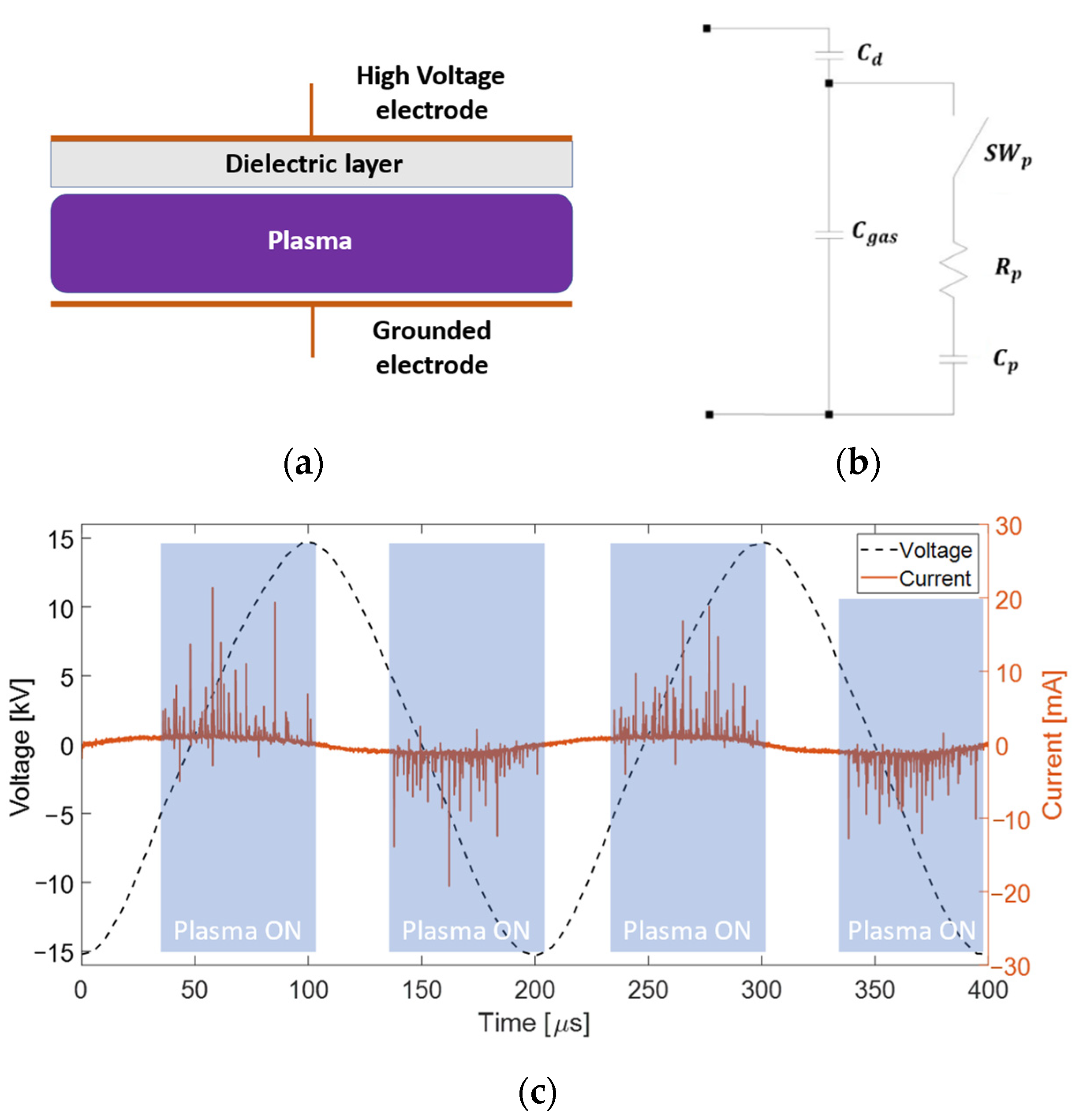
Figure 1 shows (a) a typical DBD configuration, (b) a corresponding simple equivalent circuit, and (c) the voltage–current waveform during the discharge phase (Plasma ON). The Plasma ON phase can be represented by a closing switch
(in the MHz range) that allows a current to flow through
and
Figure 1b. In this way, the reactor equivalent load rapidly changes in time. From a macroscopic perspective, the Plasma ON phase occurs twice during each voltage period. Microscopically, this phase is associated with the generation and subsequent rapid extinction of a large number of streamer discharges [
6]. This highly non-linear behavior is shown in
Figure 1c.
Dedicated power supplies are needed to provide the high voltage and frequency waveforms to operate these nonlinear and time-dependent loads. During the last decade, various power supply technologies have been presented [
7]. Sinusoidal [
8,
9], pulsed [
10,
11], and arbitrary [
12,
13] voltage waveforms are the most used. Among them, sinusoidal power sources are often preferred due to their inexpensiveness and robustness [
2,
5]. In various applications, especially in the biomedical field, it is particularly important to accomplish reliable and reproducible discharge conditions, which require the discharge parameters to be actively controlled. Moreover, since larger thermal fluxes of treated samples lead to unwanted thermal stresses, it is crucial to maintain constantly delivered power [
14]. Controlling the power transferred during the process translates into better control of the plasma chemical kinetics and temperature, ultimately providing more reliable and reproducible treatments [
15]. Automation technologies based on various feedback control strategies adopted to restrict these thermal effects to a desired level have been proposed [
16,
17,
18,
19,
20,
21]. However, the existing control strategy methods may be limited to only a few specific applications and reactor typologies. In fact, to regulate the nonlinear thermal effects of plasma on samples, these methodologies exploit plasma emitted spectra and electro-acoustic emissions, as well as direct measurement of the treated surface temperature. For many different applications, performing such measures is not always feasible and requires measuring instruments that are not always available. Therefore, we propose a cost-effective power control strategy—which is presented below—that relies on electrical and measurable real-time quantities and that can be exploited in different industrial fields.
In this work, we illustrate a power control strategy for a low-cost high voltage generator based on a push–pull converter. The employed power supply is used to produce DBD non-thermal discharges at atmospheric pressure. The developed generator allows for the control of the power delivered to the discharge in real-time. This is achieved by exploiting on-board high voltage diagnostics, using an Arduino DUE microcontroller unit.
This work is organized as follows: the architecture of the power supply is presented in
Section 2. Then, a description of the average power real-time estimation for two distinct DBD plasma reactor topologies—surface and volumetric—is given in
Section 3. In
Section 4, an explanation of the feedback control strategy is provided. The power feedback control strategy is tested experimentally on the two different reactor topologies, and the related results are discussed in
Section 5. In the same section, a comparison between the open loop and the controlled operation of the device is discussed, showing that the proposed novel control strategy is capable of following the transient temperature behavior, achieving constant average power operation.
The discussed DBD power supply and load are also studied by using a simplified circuital model, in
Section 6, to infer a physical relation between the observed reactor thermal behavior and its electrical characteristics.
2. Power Supply Architecture
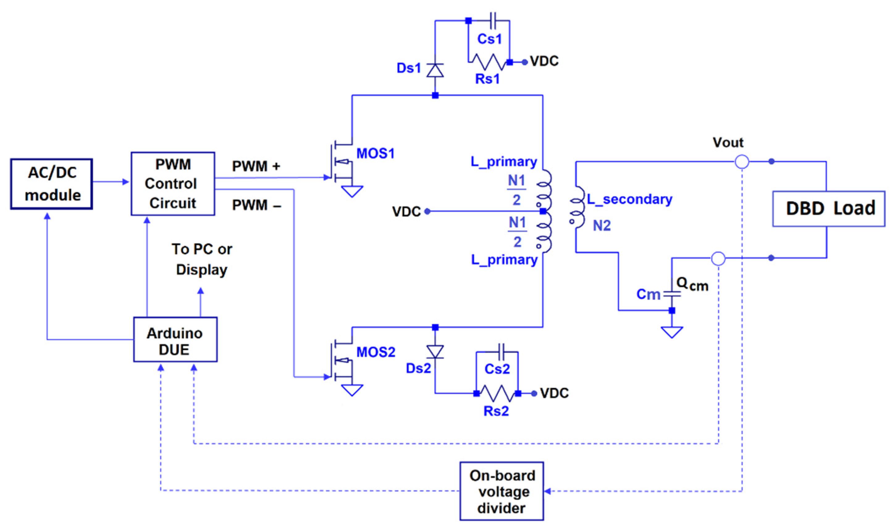
The power supply architecture is shown in
Figure 2 and described in [
6]. A push–pull high voltage ferrite transformer is used to generate sinusoidal output voltages up to a 20 kV peak with a variable frequency in the 10–60 kHz range, and with an output average power up to 200 W. A 40 DC, 10 A power source is used to supply the push–pull transformer. An Arduino DUE microcontroller (MCU) is used to control the power supply input parameters and to evaluate high voltage quantities.
The high voltage (HV) waveform supplying the reactor (
in
Figure 2) is measured by using an on-board voltage divider based on a series of capacitively compensated HV resistors. The charge delivered to the reactor is measured through the measurement capacitor
(see
Figure 2). These quantities are used to estimate the average power absorbed by the reactor through Lissajous figures [
22]. These quantities are used by the microcontroller unit (MCU) to adjust both the power supply input voltage and frequency. In this way, the HV waveform frequency is optimized based on the given rector characteristics (discussed later), and a constant average power operation of the discharge is obtained.
In previous work [
6], the self-tuning frequency control strategy, operated by this power supply, was described as follow:
A reactor is connected to the power supply;
The power supply is switched on. The MCU performs a frequency scan at ‘low’ voltage (input DC voltage equal to 2 V in this work) without igniting the discharge. For each scanned frequency, the MCU calculates the Fast Fourier Transform (FFT) of the output voltage;
Based on the collected FFT spectra, soft switching and resonant frequencies are detected.
The MCU selects and subsequently sets the optimal working frequency. This value is selected to maximize the generator efficiency and minimize the stress of the electrical components.
In this work, new features allowing for a more accurate evaluation of the average power delivered to the reactor and the possibility of achieving constant average power reactor operation will be discussed.
3. Average Power Estimation
The most important feature of the power supply described in this work is the possibility to self-regulate the average power feeding the DBD load. For real-time control, the average power must be evaluated as quickly as possible and with high accuracy. To do this, high voltage (
) and charge (
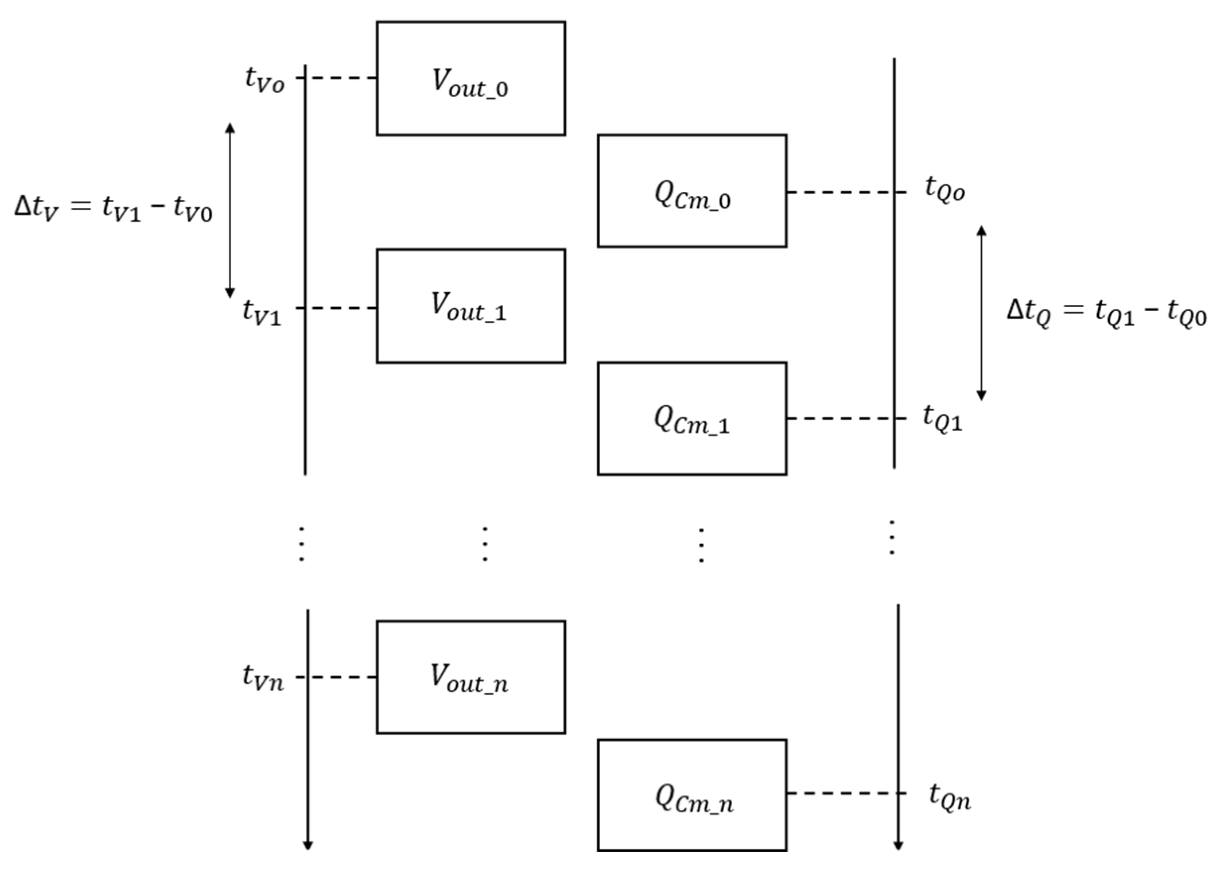
) signals are preconditioned before they are used to calculate the average power by means of Lissajous figures. The MCU measures these signals with a sampling frequency of 500 kHz by using A0 and A1 pins (ANALOG IN). The sampling procedure takes place in the following asynchronous way (see
Figure 3):
At time , the signal is sampled for the first time in the A0 Pin;
After 1 µs with respect to (), the signal is sampled in the A1 Pin;
After 1 µs with respect to (), the signal is sampled again in the A0 Pin—with a sampling time interval defined as .
After 1 µs with respect to (), the signal is sampled again in the A1 Pin—with a sampling time interval defined as .
The procedure is then repeated till the last sampling time intervals, namely and .
In accordance with the above-mentioned sampling procedure, each charge sample is acquired after the previous voltage sample, Vout_n, after a sampling time interval defined as .
This procedure is repeated acquiring 1000 samples for each Pin with a global sampling time of 2 ms.
and
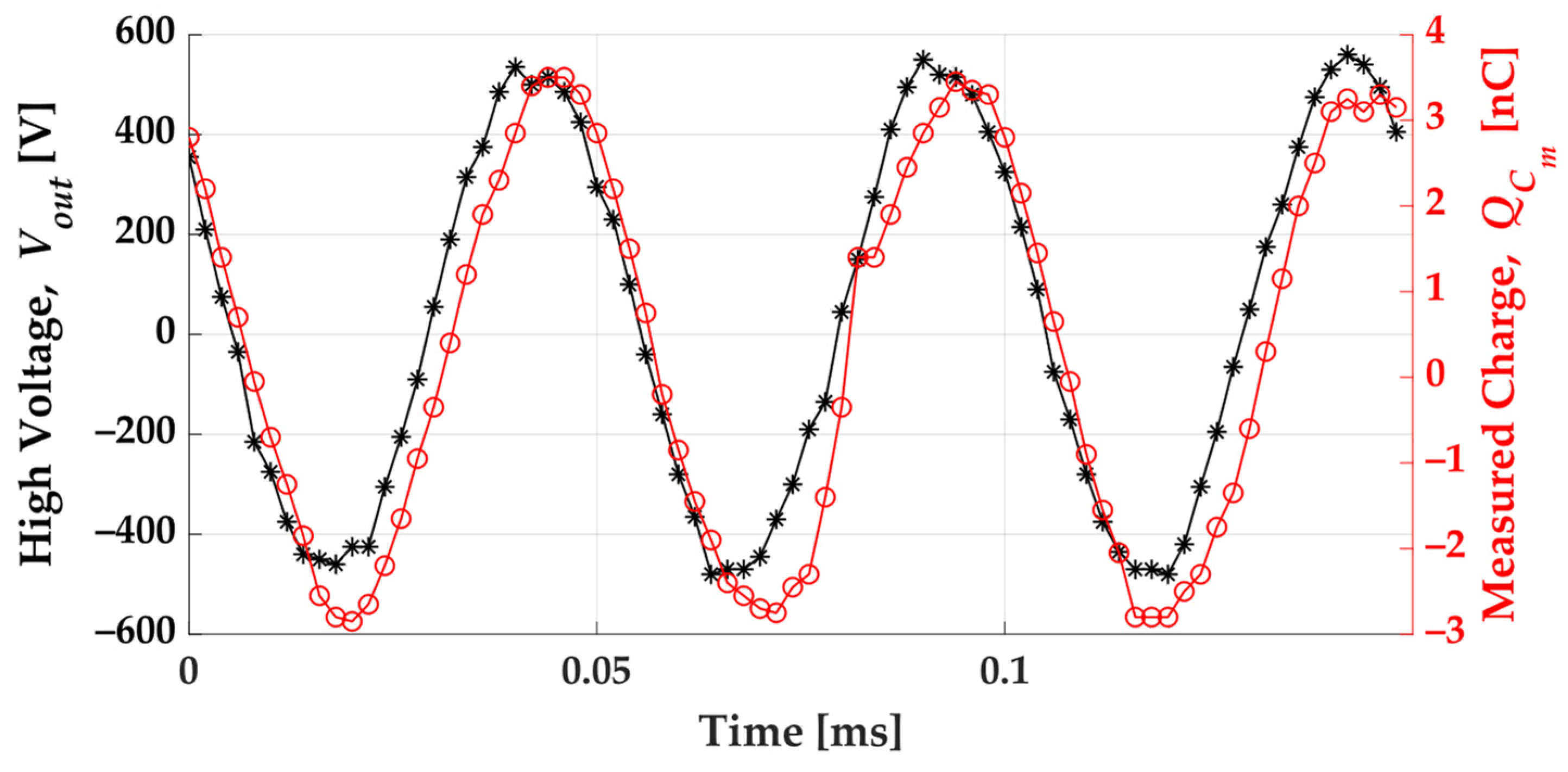
signal should be in phase (they are proportional to each other through the capacity of the reactor). As a matter of fact, these signals could be slightly out of phase due to (1) the delay introduced by different cable lengths (2) in the above-described asynchronous sampling procedure. For example, a 500 V peak, a 20 kHz high voltage waveform, and the related transported charge sampled by the microcontroller is reported in
Figure 4. On the contrary, the figure shows that the charge signal is lagging with respect to the high voltage waveform.
Thus, a first preconditioning procedure is performed to minimize the phase shift between high voltage
and charge
waveforms. This procedure automatically takes place after the establishment of the working frequency (see above mentioned self-tuning procedure points 1–4). The input DC voltage is set to 2 V. At this voltage level, the discharge does not ignite, and the corresponding Lissajous figure is expected to have a null area. The MCU acquires
and
, evaluating the Lissajous figure area (
Figure 5a). Subsequently, the MCU anticipates and delays the
array by n-samples with respect to
and calculates the Lissajous figure area. Starting from
n = 1, the procedure is repeated for increasing values of n to find the time delay yielding the minimum area. The MCU then performs all subsequent calculations with the corresponding array shift (
Figure 5b).
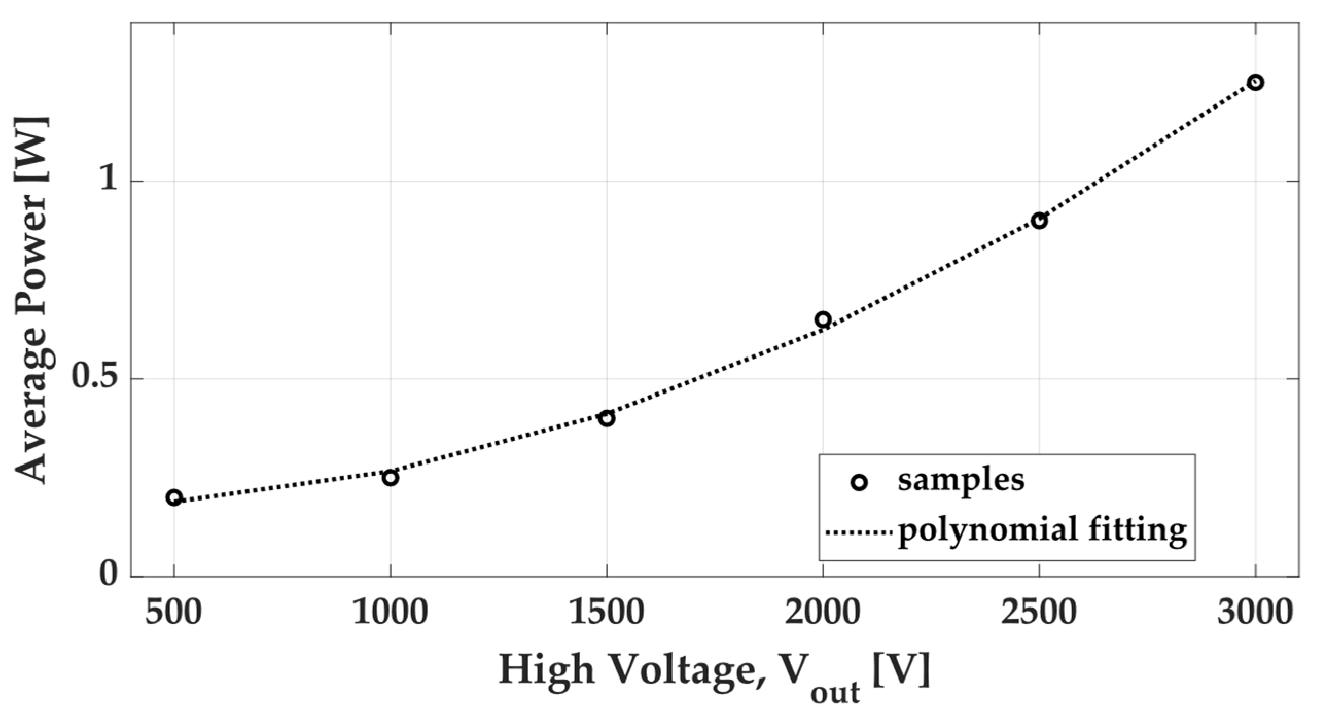
Still, further compensation of the average power evaluation is needed to account for the non-perfect zeroing of the Lissajous figure area after the delay compensation and for dielectric losses. These kinds of losses are related to dielectric hysteresis and are proportional to the square of the applied voltage (
). Hence, they become more and more important for increasing supply voltages. These phenomena are compensated by measuring the average power when the output voltage is in the range of 0.5 ÷ 3 kV. In the tested conditions, these voltages do not lead to plasma formation. An example of average power as a function of the applied voltage without discharge ignition is shown in
Figure 6. The displayed data are fitted with a second order polynomial, which is used in turn to extrapolate the average power offset for the given operational voltage.
The delay compensation and power polynomial fit allow the average power estimation accuracy to be further increased. An evaluation of the estimated average power standard deviation was carried out for a data set of 20 acquisitions. Each acquisition requires about 6 ms, of which 2 are related to the sampling of
and
, and 4 are necessary for the power calculation. The standard deviation is within 4%. This value is comparable to that obtained when using expensive and highly accurate measurement setups (oscilloscope and dedicated probes) [
6]. This demonstrates the possibility of an average power real-time estimation for DBD plasma reactors.
4. Average Power Control Strategy
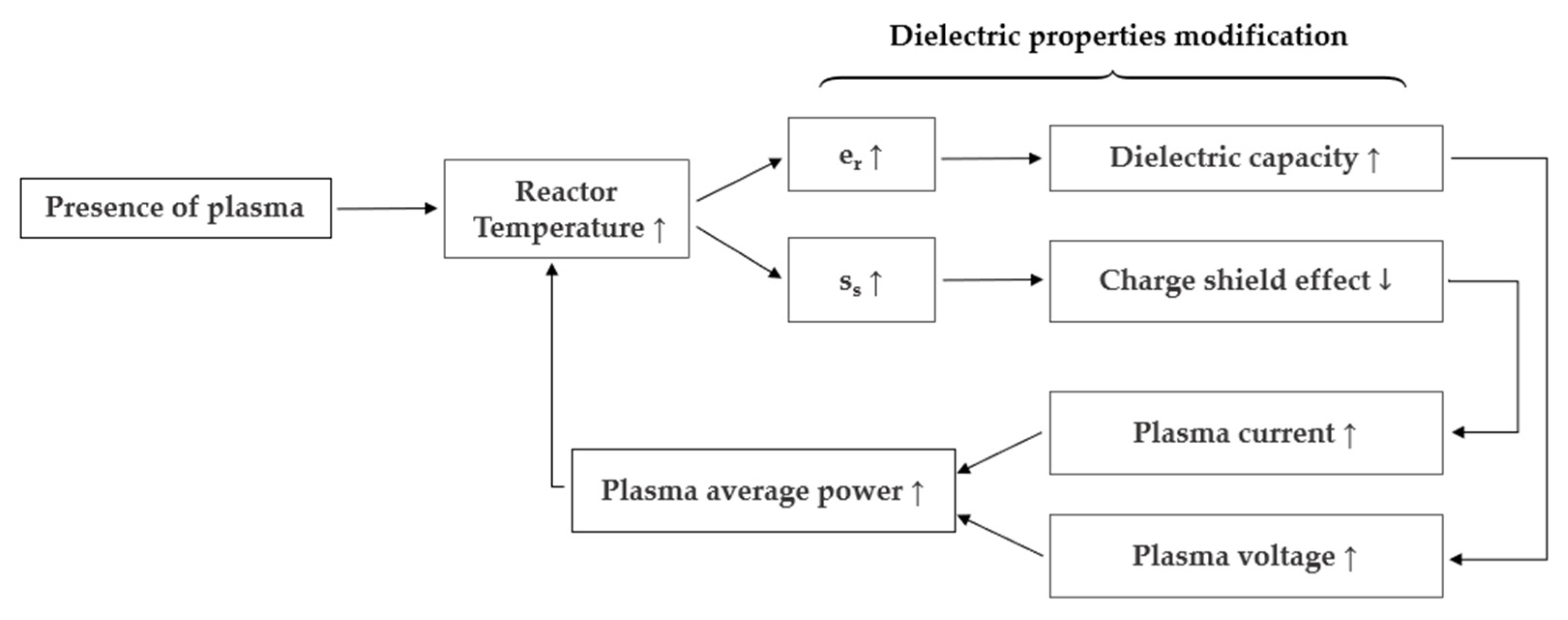
The physical behavior of DBD reactors is strongly influenced by several factors. These include the reactor geometry, the physical properties of the dielectric layers, the pressure and chemical compositions of the gas, and the reactor temperature. Since the above quantities modify the discharge characteristics, ideally these should all be controlled in real time during the reactor operation. In reality, this is unpractical because (1) many of the listed phenomena cannot be directly measured while the reactor is working, and (2) these occur over markedly different time scales. This work only focuses on temperature effects, for two different reasons. First, thermal transients take place with relatively slow temporal dynamics, i.e., hundreds of milliseconds or even seconds. Hence, since the average power can be calculated each 6 ms, these can be adequately followed by the proposed control system. Second, controlling the temperature during treatment is a technical requirement for many biomedical and industrial DBD reactor applications. Temperature increment DBD reactors are usually in the range of 20 ÷ 200 °C and are related to the presence of both the discharge and dielectric losses. When a sufficiently strong electric field is applied to a DBD reactor, the plasma is generated, and the dielectric layer temperature starts to increase (
Figure 7).
The temperature affects dielectric properties such as electric permittivity
and surface conductivity
. The former usually increases when temperature is incremented within the abovementioned interval range of 20 ÷ 200 °C (for higher temperature values, different trends can be observed depending on the given considered material). It is worth recalling that an increase of
results in a consequent increment of the dielectric layer capacitance. Surface conductivity
strongly increases with the temperature, as expressed by the following expression [
23]:
where
and α are a reference surface conductivity value and a coefficient depending on the given material, respectively.
is the temperature, expressed in Kelvin.
It is thus possible to state that electric permittivity and surface conductivity increase with the electric permittivity. A dielectric constant increment leads to growth of the generator output voltage due to the variation of the frequency response. This behavior will be better investigated and explained in
Section 5. If the applied voltage is incremented, average power delivered to the discharge will be incremented too. This power increment will increase the temperature, and this will trigger positive feedback. Moreover, growth in the surface conductivity leads to faster removal of charges stored on the dielectric surface, decreasing their shielding effect towards the externally applied field. This behavior will promote the ignition of a higher number of plasma filaments leading to an increment of the discharge current. Consequently, the average power and temperature will increase too and contribute to the positive feedback. This behavior can be observed on a large variety of DBD reactors and must be prevented if a stable, safe, and reproducible treatment is to be performed.
The average power control strategy was implemented by using the following empirical expression [
24]:
where
is the average power,
is the peak value of the applied voltage
, and
is a constant, determined by dielectric properties (material and geometry). After all the procedures described in
Section 3,
is evaluated by the MCU. After that, the system requires the operator to define a working value for the voltage chosen to suit the reactor characteristics and specific treatment. At this point, the operator chooses between a manual (MAN) or automatic (AUTO) operation. MAN corresponds to an open-loop, where a constant VDC voltage is used throughout the entire treatment. If the AUTO operation is selected, the user-defined
is marked as
and the corresponding measured average power as
.
will be used as a reference during the entire treatment. At the i-th iteration, the measured average power is be compared to
P0, finding a power error Δ
P =
P0 −
Pi. If |
| exceeds the reference power error
, a voltage error
is calculated according to Equation (2) and is used by the MCU to consequently modify the input DC voltage. The standard deviation in the average power measurements is within 4% (as mentioned above). Consequently, the reference power error
is set to 5% of
.
5. Average Power Feedback: Test Cases
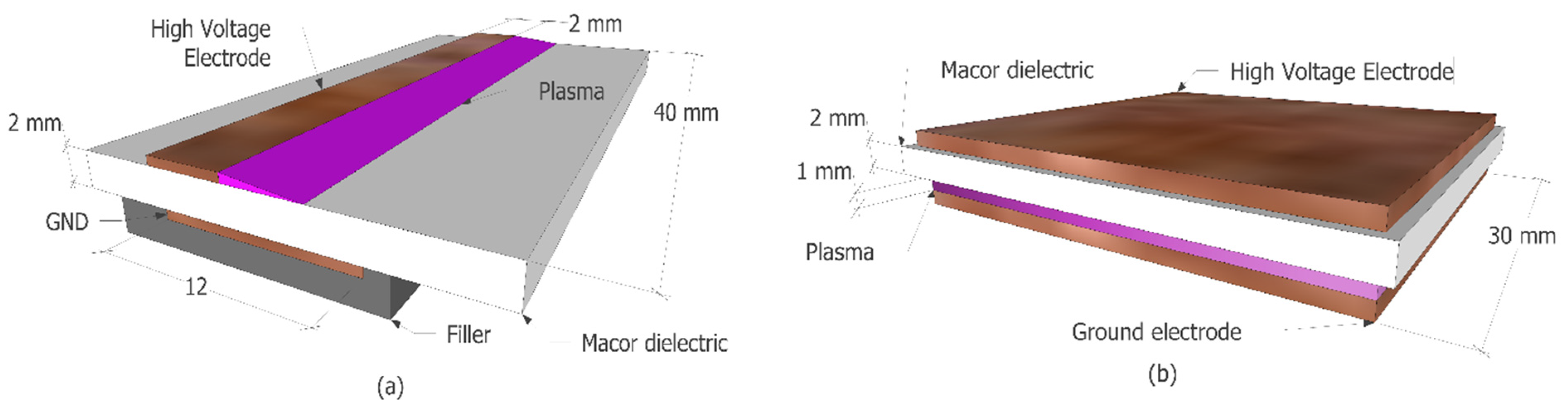
In this section, the ability of the power supply to feed DBD loads with constant average power is shown for two different reactors. The considered DBD reactor geometries and dimensions are shown in
Figure 8. Both reactors used a 2 mm thick Macor dielectric layer and were supplied with a 31 kHz sinusoidal voltage waveform (
). Both devices were operated with atmospheric pressure air. In
Figure 8a, a surface reactor with an asymmetric electrode configuration is depicted. This reactor was supplied with a 7.5 kV peak voltage
and an average power of 8 W, leading to a power density of 2 W/cm. In
Figure 8b, a volumetric reactor with a squared electrode geometry is shown. This reactor required a higher voltage to ignite the discharge, i.e., 10.4 kV peak, yielding an average power of 29 W and a power density of 3 W/cm
2. These rather severe supply conditions were chosen in order to induce strong thermal stress into the dielectric layer, leading to marked average power variations.
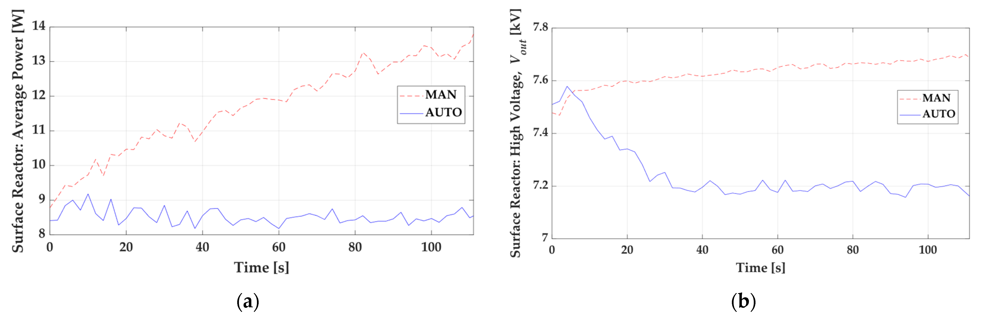
Figure 9a shows the average power feeding the surface reactor as a function of time, without (MAN) and with (AUTO) the described feedback control. When the system was operated in the MAN condition, the thermal effects increased the average power as time went by, causing the average power to increase by about
after 110 s. Conversely, when the system was operated in AUTO mode, the average power was kept constant by the MCU; see the blue continuous line in
Figure 9a. Power variations were comparable to the power measurement standard deviation (4%). The corresponding supplied peak voltage is shown in
Figure 9b for both modes. In the open loop mode (MAN), the supplied voltage increased by about 3% due to variations in the equivalent load impedance. In the closed loop mode (AUTO),
automatically decreased over time to follow the reference average power value.
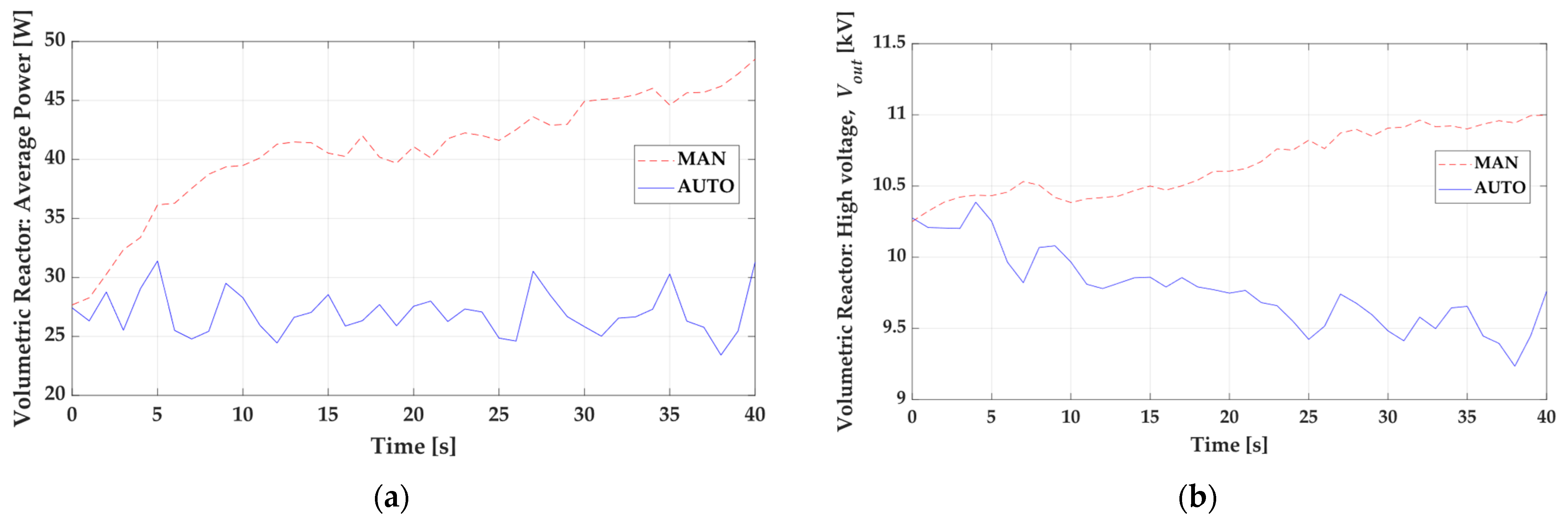
Similar trends were observed for the volumetric reactor. As shown in
Figure 10a, the average power in the MAN condition increased by about 78% during the first 40 s of operation. Note that this increment was significantly faster compared to that exhibited by the surface reactor. Hence, the volumetric geometry could suffer severe damage or rupture over longer time periods. On the other hand, when the generator was operated in AUTO mode, the average power was maintained at a roughly constant value. These results were obtained by allowing the MCU to dynamically adapt the supply voltage (
Figure 10a). Conversely, the high voltage peak value
Vout increased by about 12% in MAN mode (
Figure 10b).
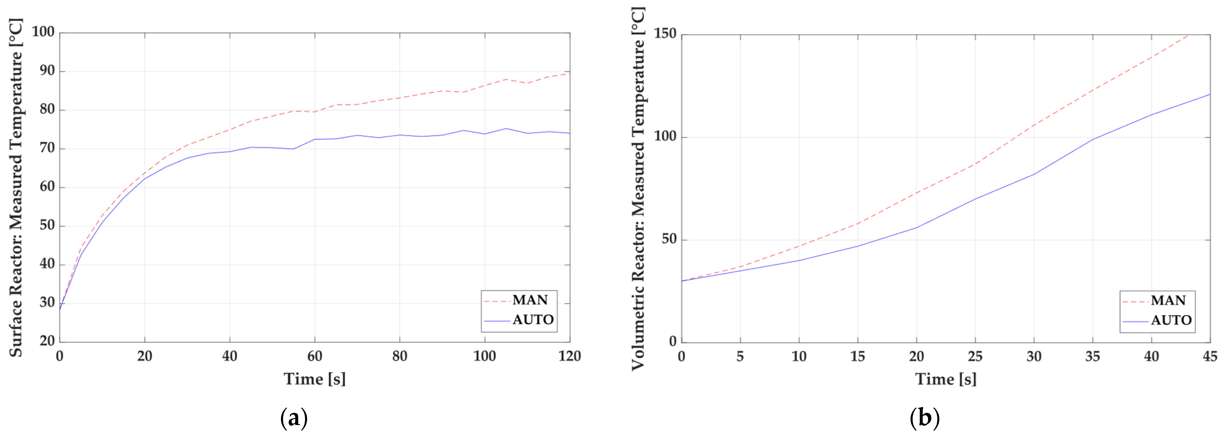
The influence of the average power control on the reactor temperature was also investigated. The reactor’s temperature was measured by means of a FLIR SC640 infrared camera. The results for the MAN and AUTO conditions are displayed in
Figure 11. The reported data refer to the temperature of the Macor layer measured near the high voltage electrode. Regarding the surface reactor, this value represents the highest temperature reached by the reactor itself. Conversely, for the volumetric reactor, the measurement underestimates the maximum temperature reached by the Macor layer in contact with the discharge. Indeed, it was not possible to perform a real-time temperature measurement within the plasma volume without switching off the discharge and opening the volumetric reactor.
The temperature variations displayed in
Figure 11a refer to the surface reactor. Operating the generator in AUTO mode allowed the dielectric temperature to be reduced by about 20% after 110 s of discharge. It is worth noting that the temperature differences in MAN and AUTO modes were negligible within the firsts 20 s of operation. This is related to the dynamics of the thermal transient caused by the discharge, releasing thermal energy to the dielectric. The corresponding measurements on the volumetric reactor are reported in
Figure 11b. Unlike what was observed for the surface reactor, here the temperatures in AUTO and MAN modes started to differ once past 5 s. This is because in the volumetric geometry, the plasma volume was confined within the reactor, and the discharge released thermal energy to the dielectric more efficiently. After 45 s of discharge, the AUTO mode showed a temperature decrement of about 30%.
6. Equivalent Circuit Thermal Analysis
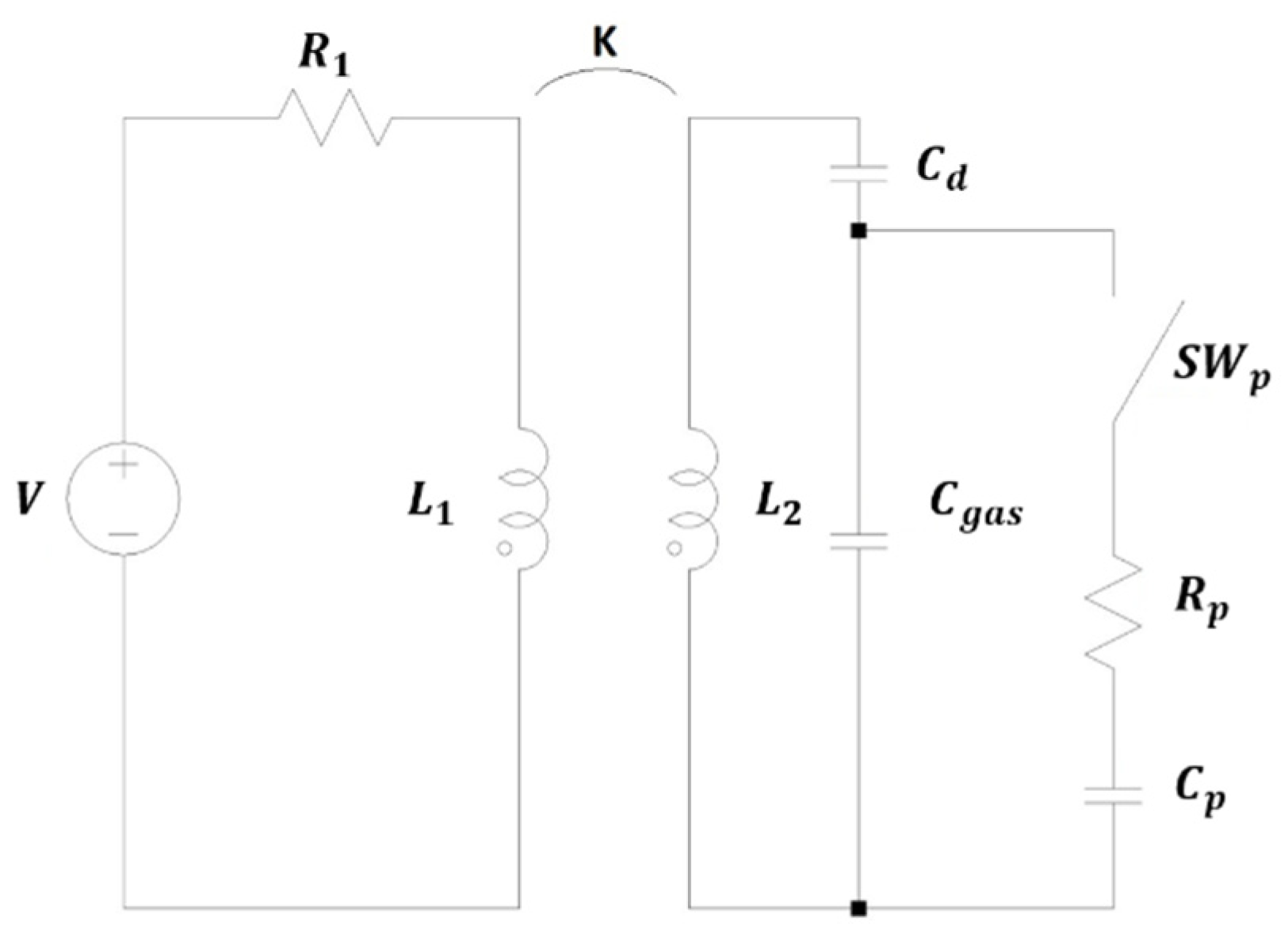
At this point, it is worth investigating why the reactor equivalent load impedance is modified by temperature variations, and how this affects the output voltage. The power supply and DBD reactor equivalent circuit are shown in
Figure 12 [
25]. The power supply can be schematized with an internal resistance
and a transformer with primary and secondary inductances, L
1 and L
2, respectively. In the DBD load,
and
represent the dielectric and gas capacities, respectively. As already introduced, when a streamer is generated in the gas bulk, the switch
is closed, introducing a plasma resistance
and capacitance
in parallel to
. The switch commutates in the megahertz range to represent the characteristic dynamics of streamer discharges [
26].
In
Section 4, the relationships between temperature and both capacitance and surface conductivity were introduced (see Equation (1)). In this work, Macor ceramic was used as the solid dielectric. This material exhibited negligible electric permittivity variations in the considered operation conditions and when temperature was varied in the above-mentioned range of 20 ÷ 200 °C [
27]. Despite this, the reactor equivalent capacity was strongly modified by the presence of the plasma. Indeed, when the discharge was ignited, the equivalent capacitance was increased with respect to the gas capacitance,
, due to the generation of charged species in the gas bulk. Increments of the surface conductivity,
, with temperature led to a denser plasma and, in turn, to a higher equivalent plasma capacitance. Thus, it is possible to infer that by increasing the reactor temperature, the equivalent plasma capacitance is also increased.
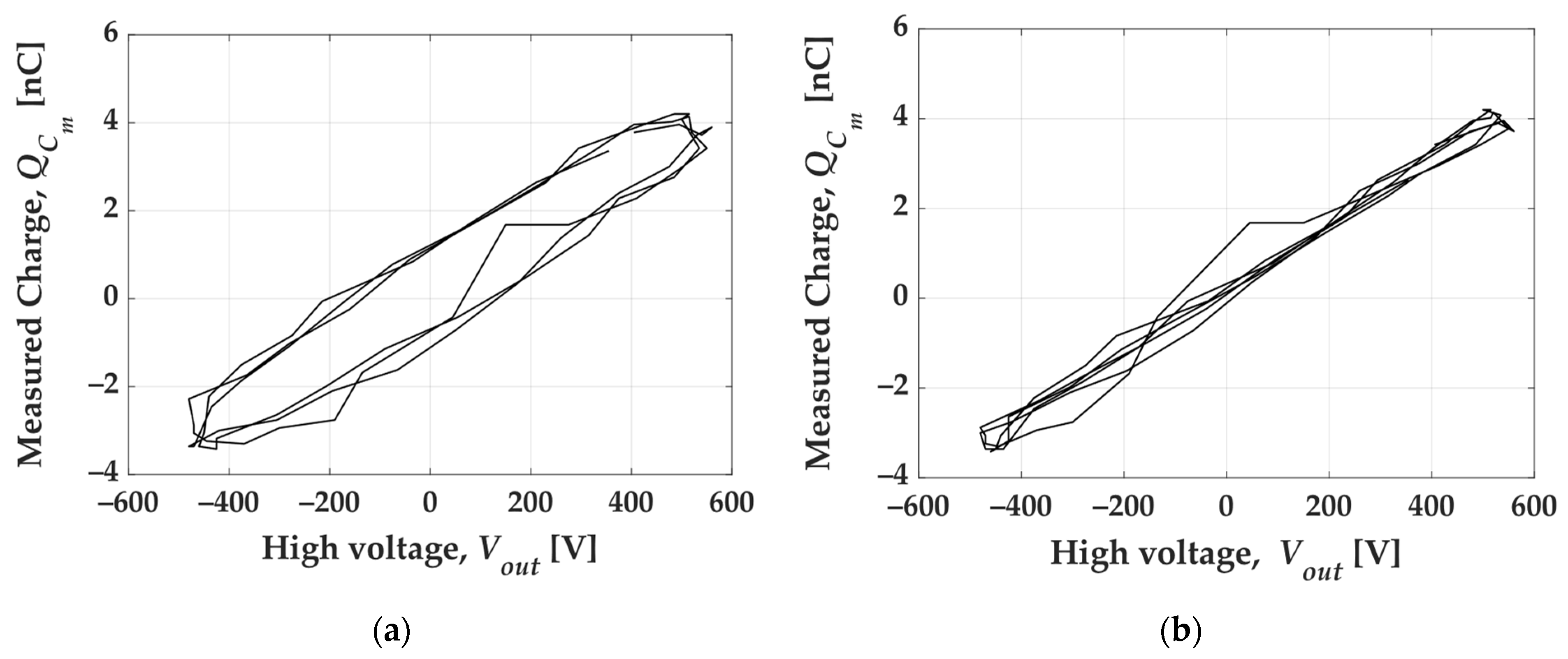
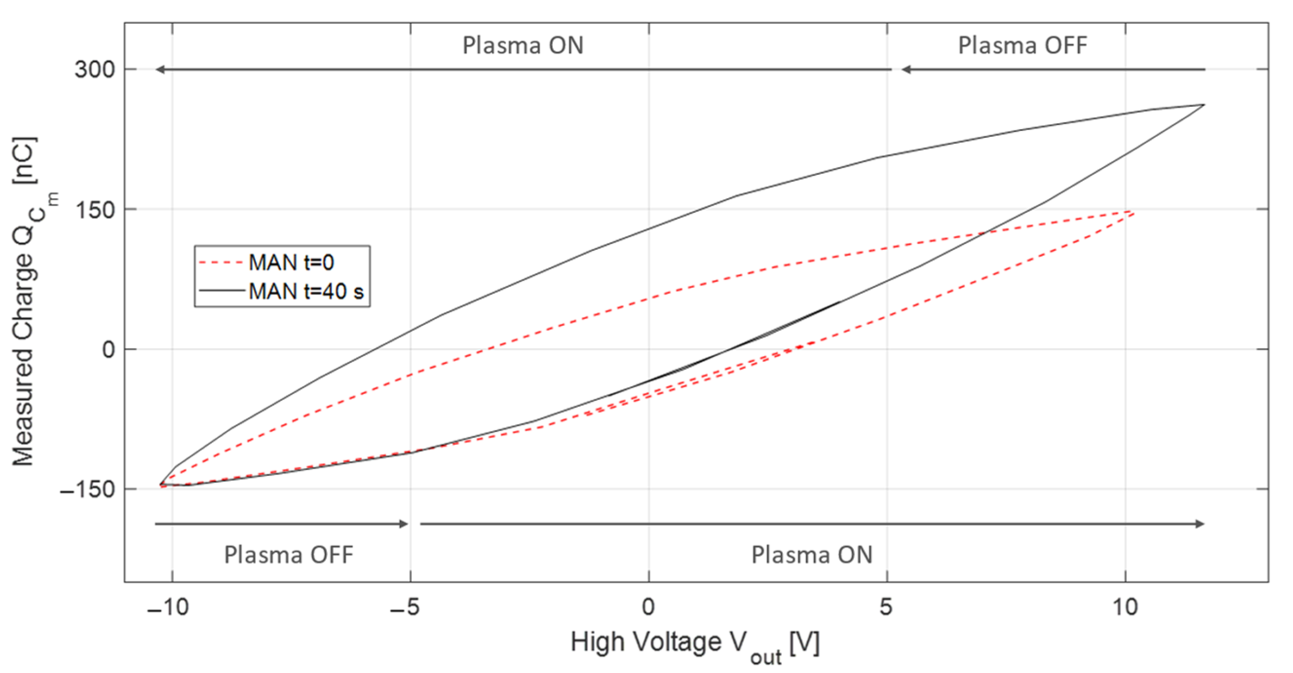
This behavior can be experimentally observed in
Figure 13 by comparing the Lissajous figure measured for the volumetric reactor both at the first ignition of the discharge (MAN
s) and after 40 s of the discharge condition (MAN
s). The two Lissajous figures were plotted overlapping the left bottom corner for visual and intuitive comparisons. In
Figure 13, two different sections of the Lissajous curve are highlighted. The one marked with ‘Plasma OFF’ refers to voltage intervals where the discharge is not ignited. On the contrary, ‘Plasma ON’ portions are related to voltage intervals where the discharge is present. It is worth pointing out that the slope of the Lissajous figure represents the equivalent load capacity at a given applied voltage [
22].
Starting the study of the two figures in the bottom left corner, it is possible to infer that ‘Plasma OFF’ portions for both curves are about the same in length and slope. Hence, when the discharge was not ignited, the equivalent reactor capacitance did not change with time, and its dependence on temperature could be neglected in the investigated temperature range. This behavior is consistent with the negligible influence of the temperature in the Macor dielectric permittivity, as already described. When the discharge was macroscopically ignited, in the ‘Plasma ON’ portions, the Lissajous curve slope rose smoothly (
Section 1). This resulted in the proportional growth of the equivalent reactor capacitance. A different increment was observed for the two operation conditions—at
s, and at
s. In fact, in the latter condition, a higher equivalent reactor capacitance could be observed. As discussed above, this trend may be related to the increment of surface conductivity,
, as temperature gradually rises.
This behavior was investigated from a circuit point of view by using the free LTSpice software [
28]. The circuit reported in
Figure 12 was implemented in LTSpice for both reactors. In the following, only the volumetric reactor results are displayed, since this reactor exhibited greater variations in both the supplying voltage and average power, induced by temperature variations (see MAN values of
Figure 9 and
Figure 10).
The circuit simulation was carried out in the frequency domain. In order to simplify the procedure, the switch,
, was kept closed. The generator and switched-off reactor parameters were measured by using an Asita AS250 impedance meter (see
Table 1). Mutual inductances in LTSpice were expressed by means of coefficient
(
Figure 12). This was set to 0.94 in this work according to [
6].
The plasma resistivity and capacitance,
and
, respectively, were adjusted by comparing the measured quantities (
and average power) with simulation outputs (see
Table 2).
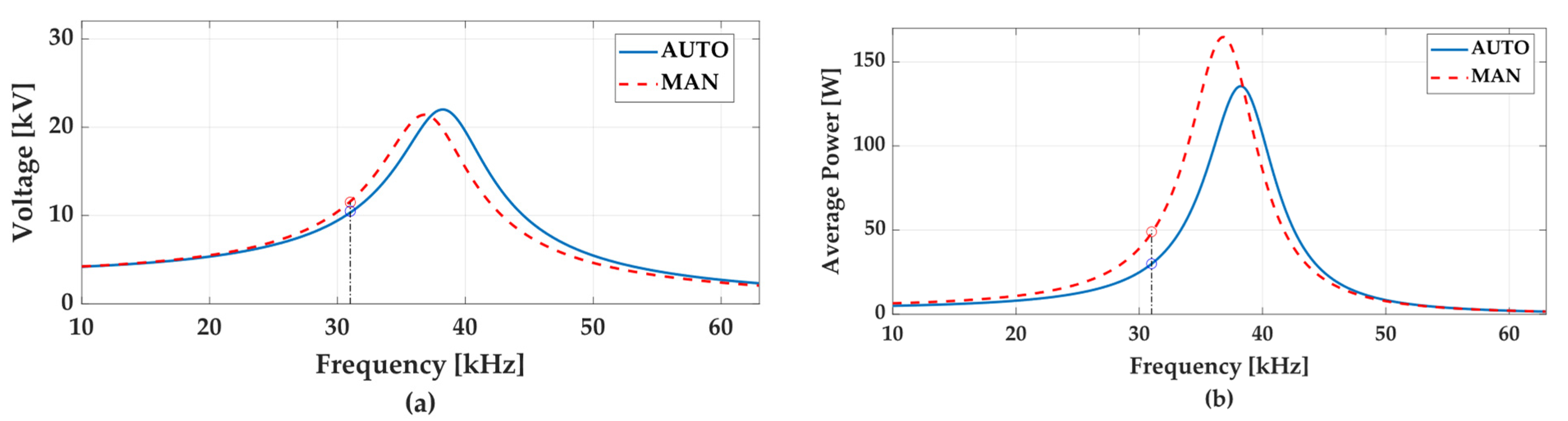
Using the implemented equivalent circuit model, the frequency response of the system was evaluated between 10 and 60 kHz. The output voltage,
, and the average power feeding the discharge (i.e., absorbed by resistance,
) are shown in
Figure 14 for
s and
s, respectively. In both graphs, the vertical black dashed line indicates the working frequency, which was equal to 31 kHz.
The voltage response was mainly affected by the plasma capacitance value (). For a constant working frequency, increasing resulted in a lower resonant frequency of the system, finally leading to a increment. The plasma resistivity, , was related to the produced plasma density. Indeed, denser plasma yielded a higher electrical conductivity. Variations of the plasma resistance, in the circuit model mainly affected the obtained average power. Indeed, a decrement of increased the average power delivered to the discharge.
7. Conclusions
This work deals with the implementation of a control strategy for a Dielectric Barrier Discharge (DBD) reactor high-voltage power supply. DBD reactors are time-dependent and nonlinear loads, and there is a growing technical need for reliable and reproducible treatments, which require the discharge parameters to be actively controlled. In this spirit, a novel control strategy is presented aiming to achieve constant average power operations of different types of DBD reactor loads. The proposed strategy exploits on-board high voltage diagnostics and an Arduino DUE microcontroller to perform real-time evaluation of the average power delivered to the load. This quantity is evaluated every 6 ms. A control algorithm based on an empiric expression relating the power delivered to the load to the power supply output voltage is presented and implemented. In the developed power supply, the average power is kept constant by the microcontroller unit by dynamically varying the input DC voltage of the generator. The performed experimental measurements show that the developed power supply is capable of controlling the average power for different configurations, i.e., a surface and a volumetric DBD reactor topology. In the controlled operation, the measured power stays within of the reference value for both configurations. It is also shown that—if the DBD reactor is powered without a dedicated control strategy—unwanted temperature increases are obtained, caused by absorbed average power growth over time. These are harmful to the reactor itself, on one hand, and can invalidate the effectiveness of the provided treatments, on the other. The latter are, in turn, due to time-variations of the electric properties of the dielectric layers. The performed measurements show that the implementation of the described control strategy allows the reactor temperature to be decreased by 20% (surface reactor) and by 30% (volumetric reactor) compared to when the power supply is operated in open-loop mode. Further future developments of the described control strategy will include increasing the power supply dynamics and implementing a feedback algorithm using a PID controller.
Finally, further optimization of the control strategy is currently taking place, trying to increment generator dynamics, and working on the feed-back algorithm by introducing a PID control.


