
Efficient Circuit Structure Analysis for Automatic Behavioral Model Generation in Mixed-Signal System Simulation

 , ,
, ,
Abstract
1. Introduction
- In order to deal with the complexity of real industrial mixed-signal designs, a hierarchical structure recognition methodology for both digital and analog circuits is proposed. Because most simple cases are solved in early stages by quick methods, only a few cases are required to be compared carefully in late stages for accuracy. Combined with the proposed circuit encoding scheme for fast screening, this methodology not only significantly reduces the comparison time but also improves the search efficiency by supporting simultaneous comparison with multiple blocks.
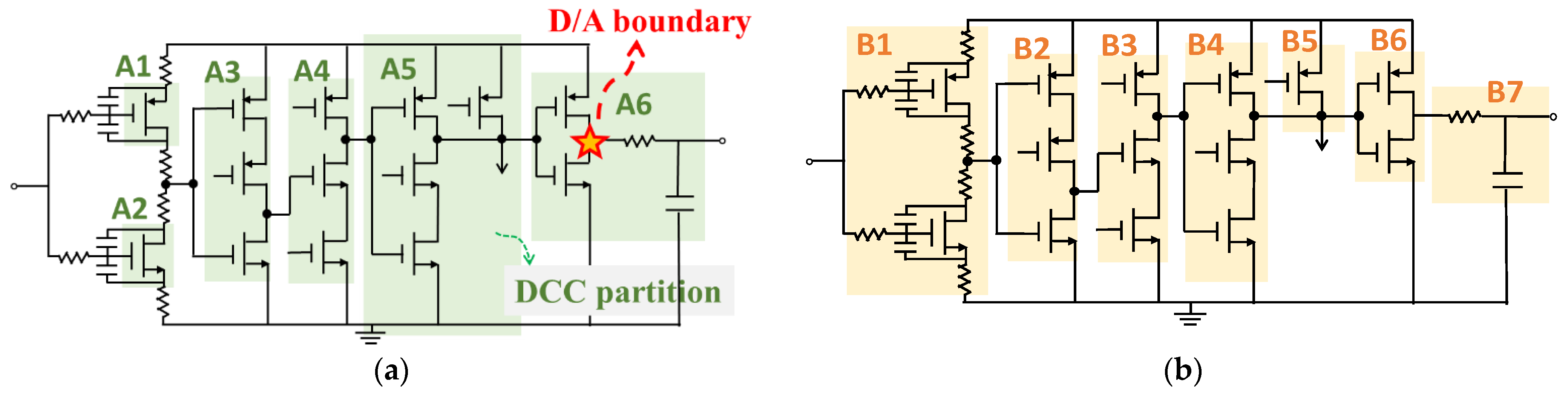
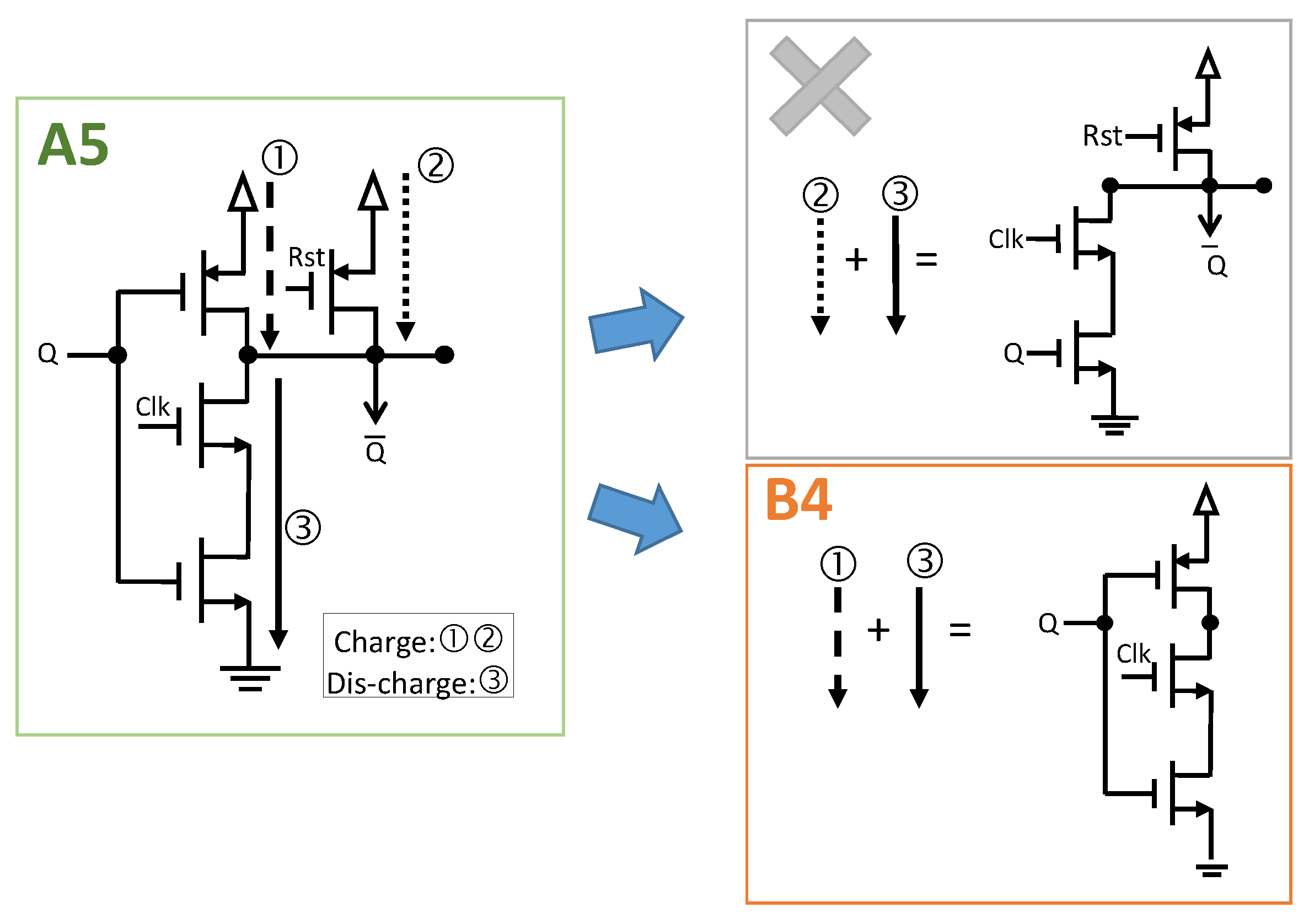
- In order to improve the accuracy for the cases where analog and digital structures are mixed together, this work considers the original design hierarchy and proposes an enhanced DCC partition method based on current path analysis. This is an efficient and accurate approach to recognize both standard CMOS cells and non-standard structures. Non-transistor devices, such as resistors and capacitors, are also properly replaced by an equivalent DC model to avoid misleading results. This feature can help identify more equivalent cells with similar structures.
- In order to support hundreds of standard cells and various circuit structures in real industrial designs, the proposed methodology leaves enough flexibility for users to add the blocks they like to increase the recognition capability, no matter whether the block is composed of analog or digital circuits. A bottom-up recognition process with redundancy removal is also proposed to support compound custom structures. This feature further increases the feasibility of the proposed methodology on real designs.
2. Background
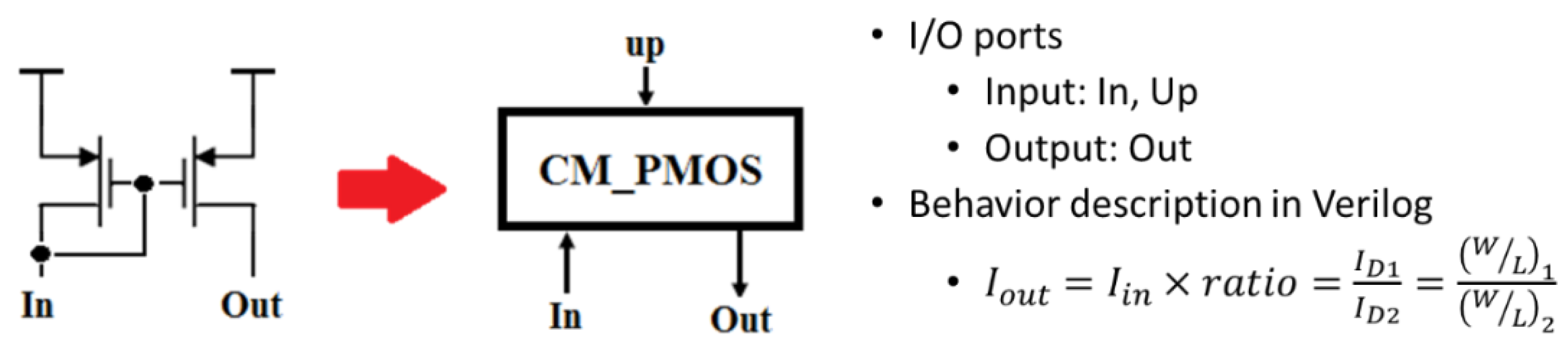
2.1. Behavioral Modeling for Analog Circuit
2.2. Structure Recognition
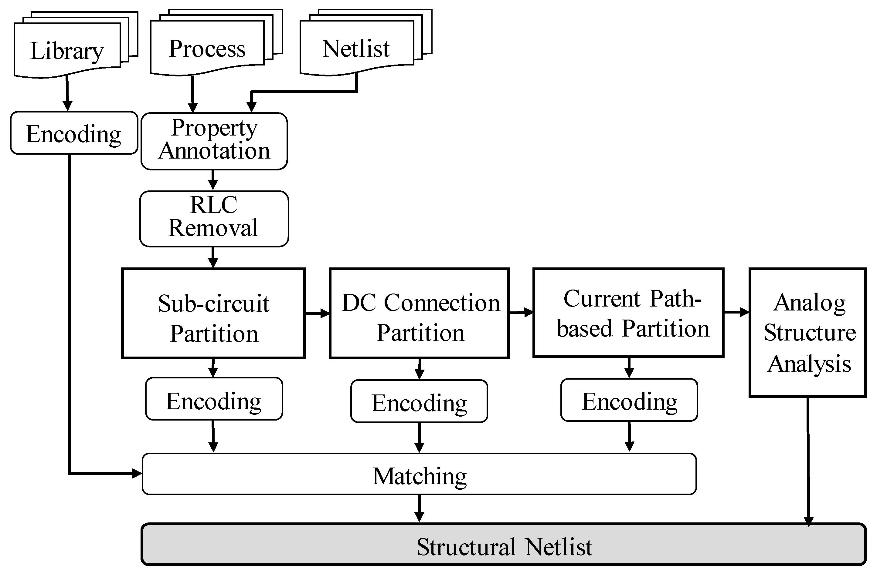
3. Pre-Processing and Circuit Encoding
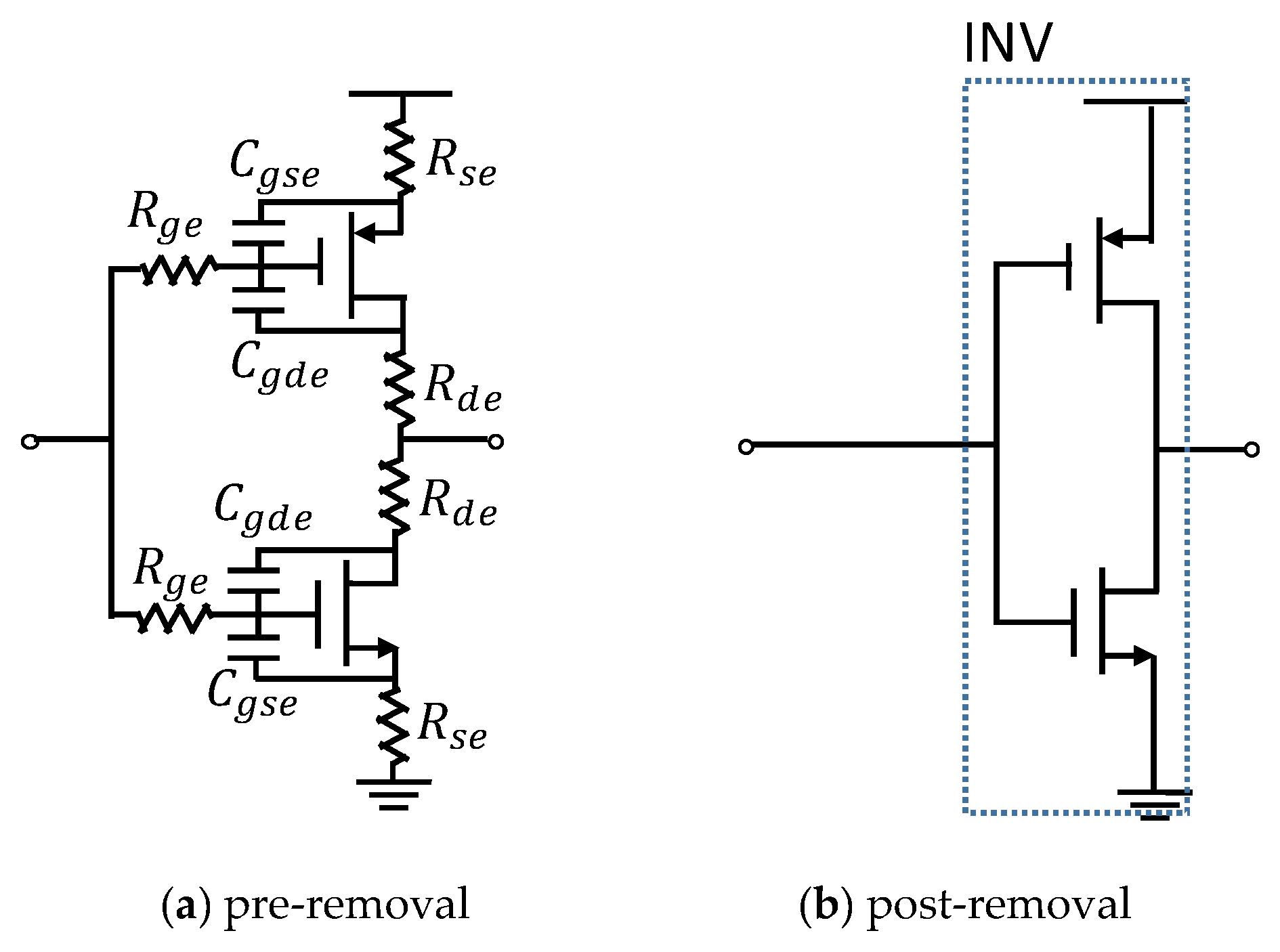
3.1. Property Annotation and RLC Removal
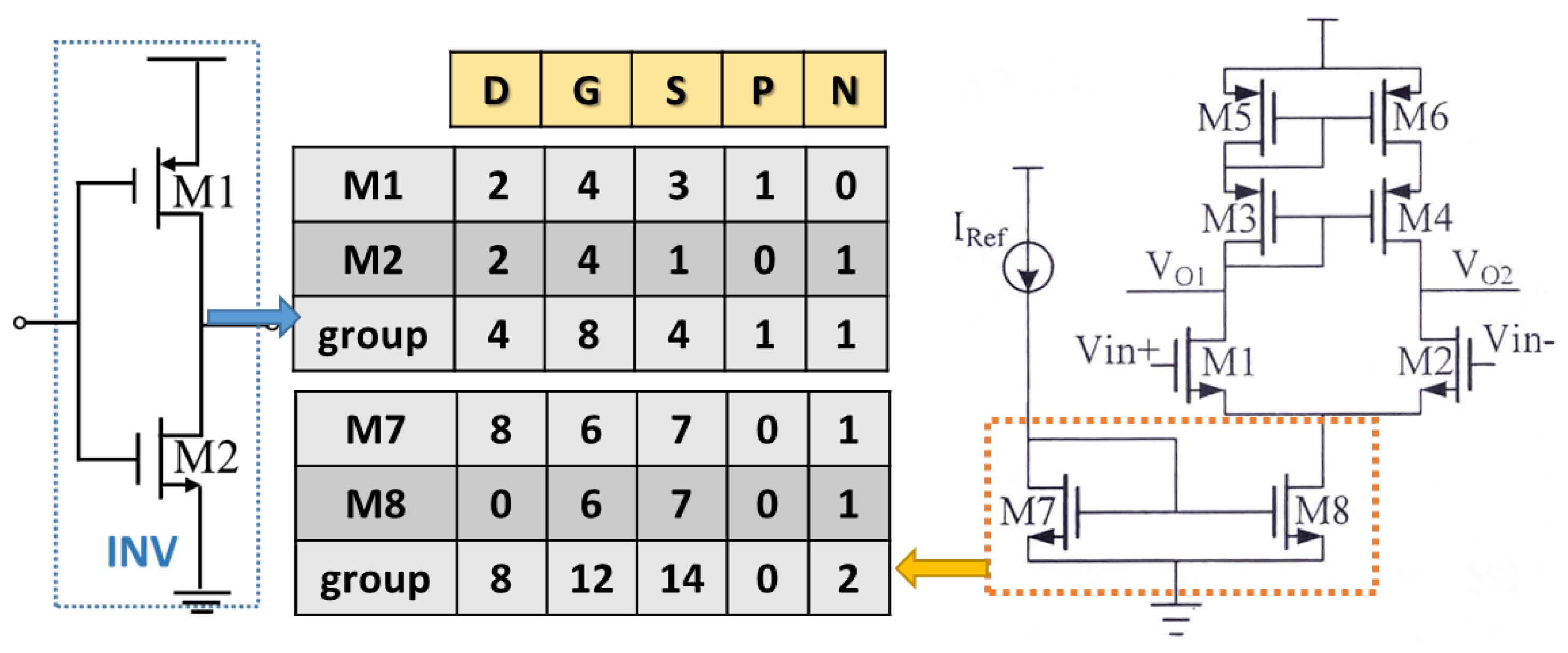
3.2. Circuit Encoding Scheme
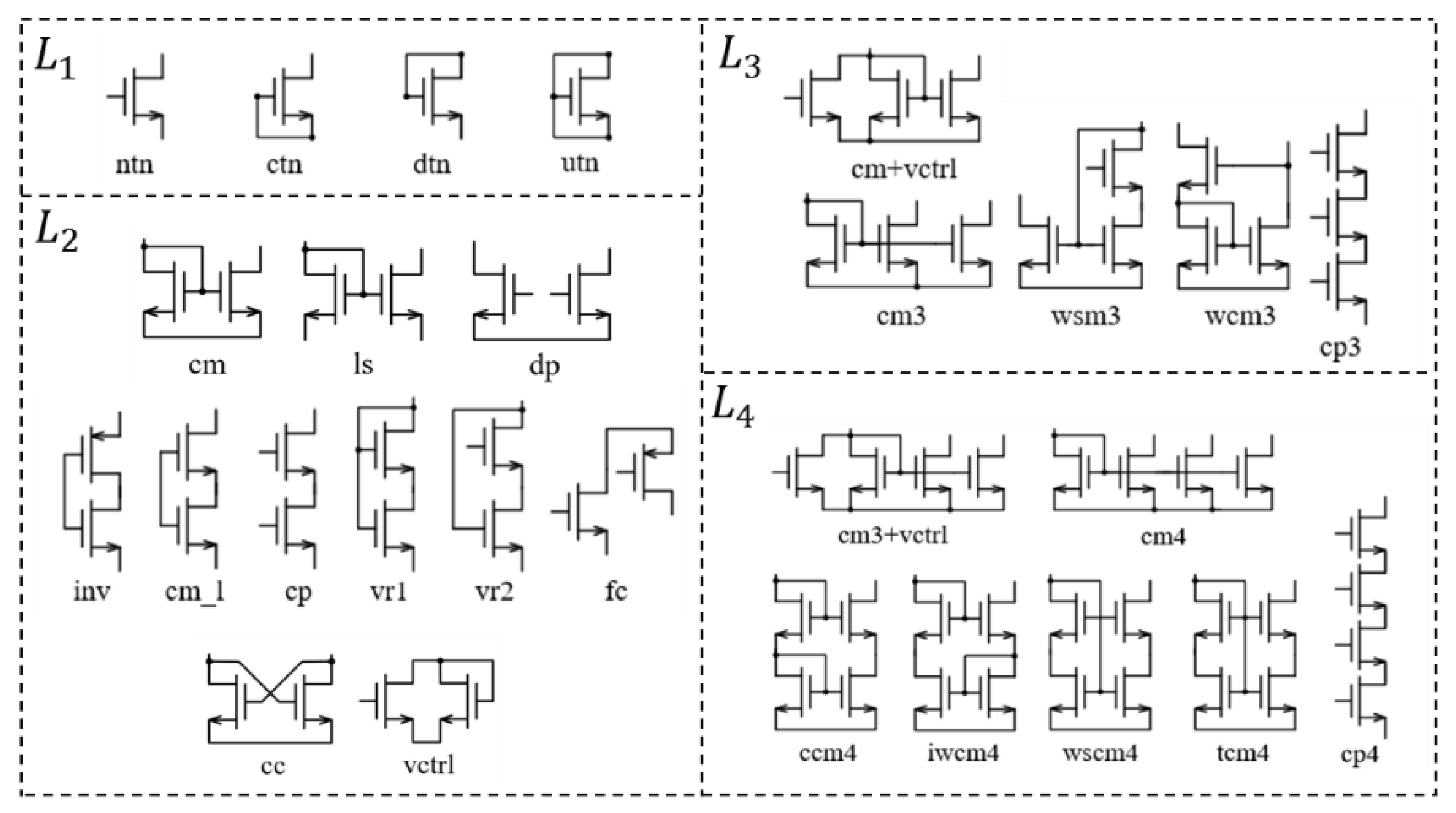
3.3. Structure Library for Matching
4. Hierarchical Structure Recognition
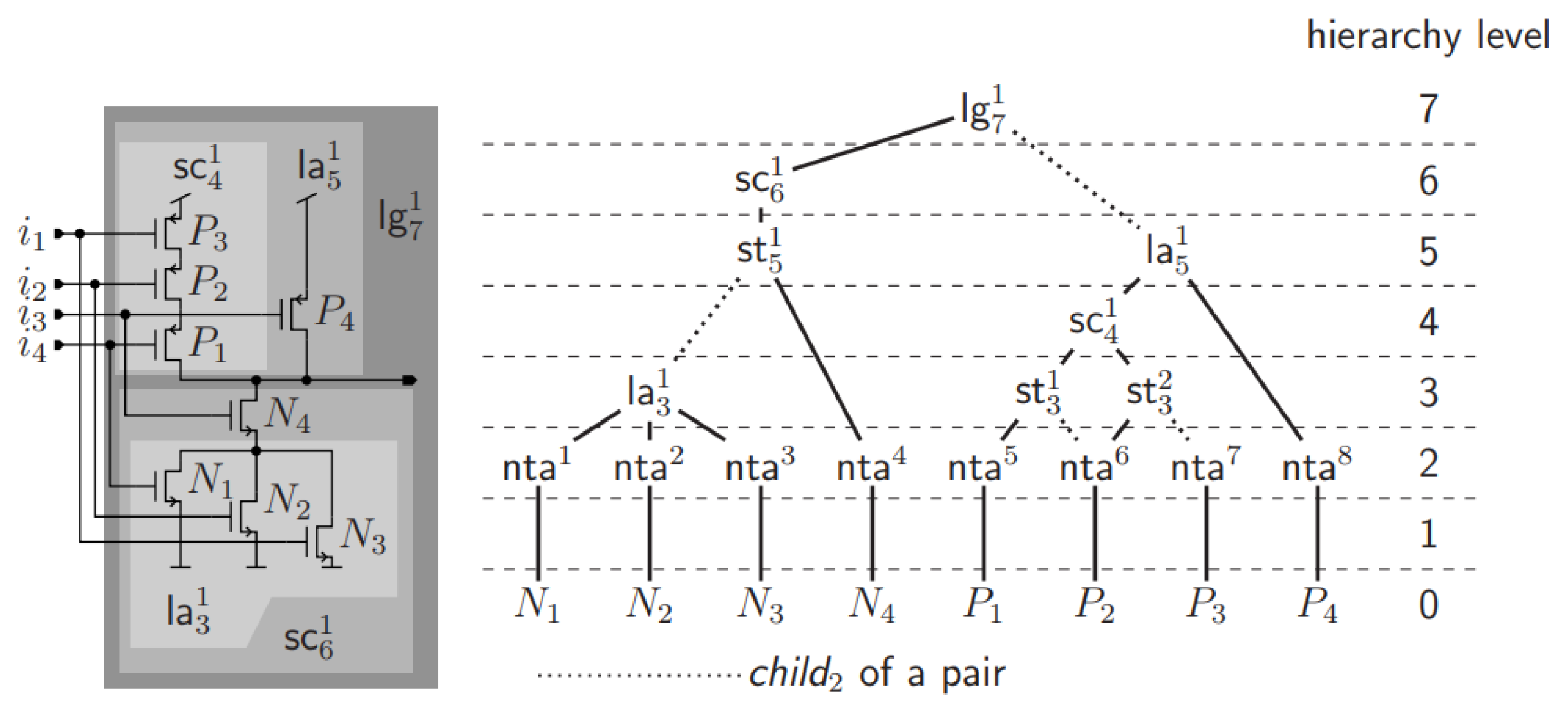
4.1. Sub-Circuit Identification
4.2. DCC Matching and Current Path Analysis
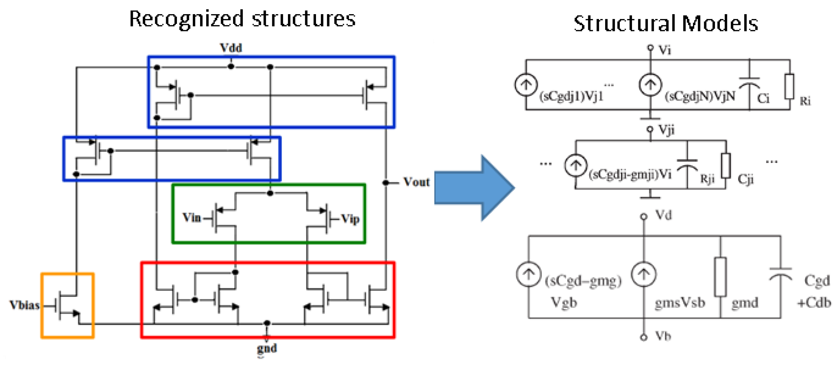
4.3. Analog Structure Analysis
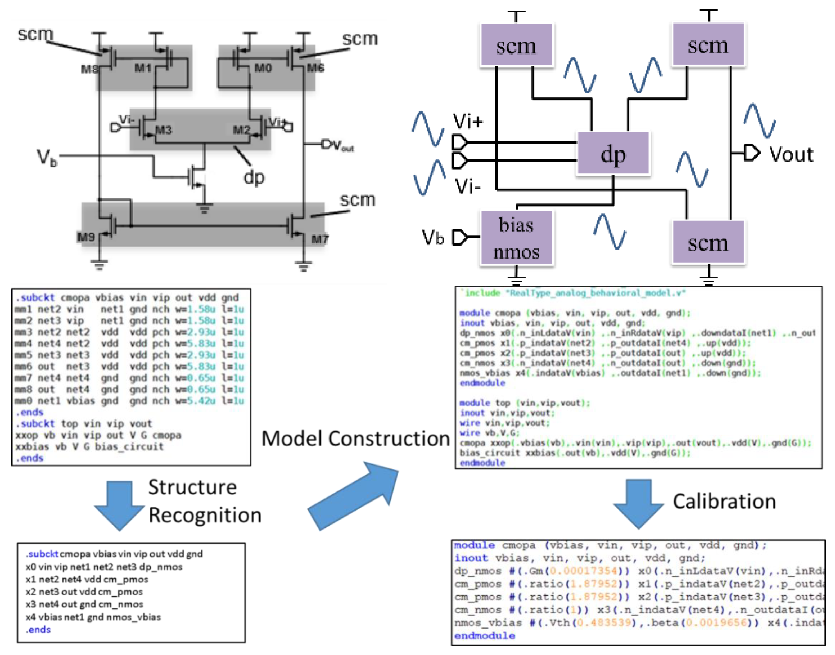
5. Application on Behavioral Model Generation
6. Experimental Results
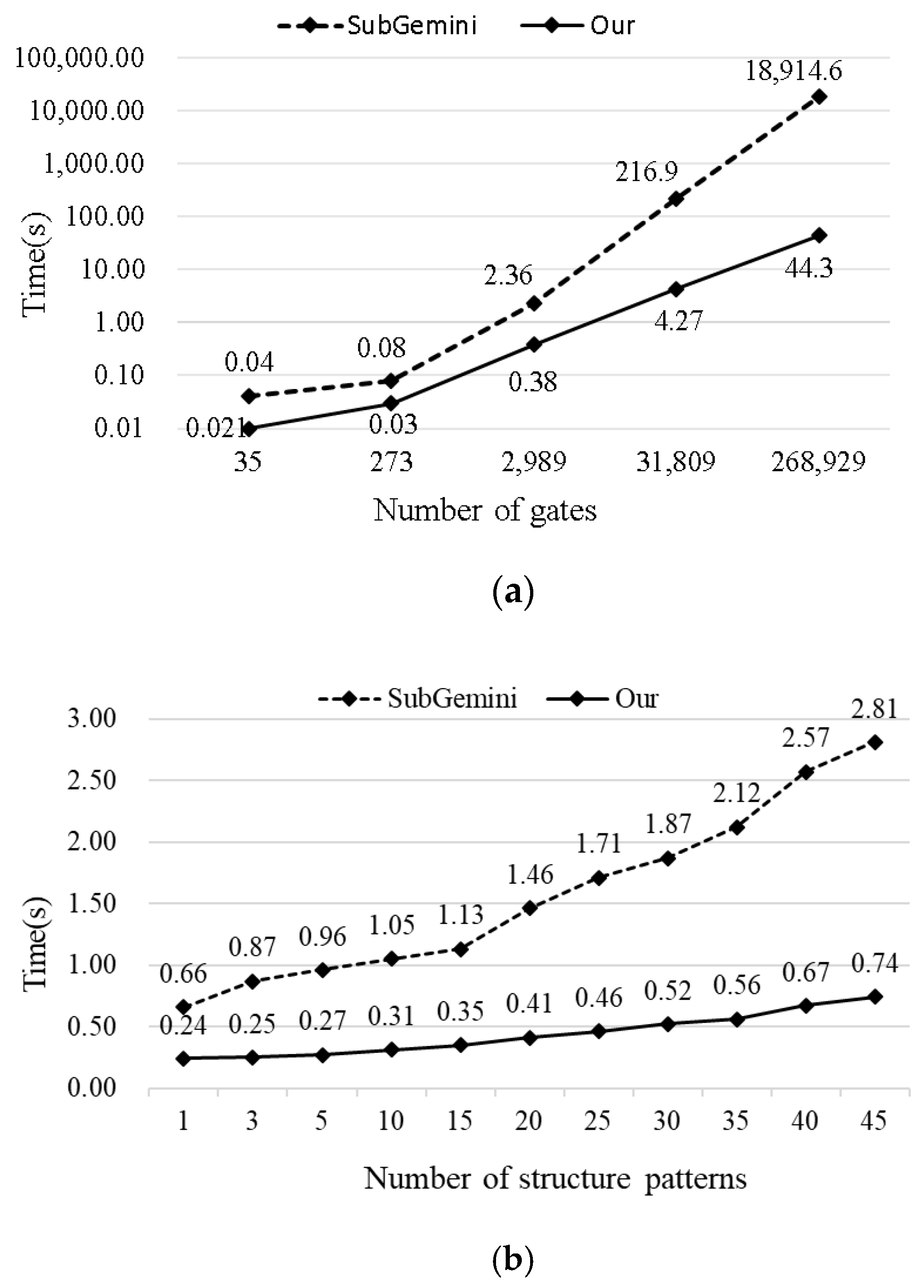
6.1. Complexity Analysis of the Proposed Methodology
6.2. Verification of Industrial Cases
7. Conclusions and Future Works
Author Contributions
Funding
Conflicts of Interest
References
- Fahmy, A.; Liu, J.; Kim, T.; Maghari, N. An All-Digital Scalable and Reconfigurable Wide-Input Range Stochastic ADC Using Only Standard Cells. IEEE Trans. Circuits Syst. II Express Briefs 2015, 62, 731–735. [Google Scholar] [CrossRef]
- Liu, J.; Park, B.; Guzman, M.; Fahmy, A.; Kim, T.; Maghari, N. A Fully Synthesized 77-dB SFDR Reprogrammable SRMC Filter Using Digital Standard Cells. IEEE Trans. Very Large Scale Integr. Syst. 2018, 26, 1126–1138. [Google Scholar] [CrossRef]
- Park, J.-E.; Hwang, Y.-H.; Jeong, D.-K. A 0.5-V Fully Synthesizable SAR ADC for On-Chip Distributed Waveform Monitors. IEEE Access 2019, 7, 63686–63697. [Google Scholar] [CrossRef]
- Aiello, O.; Crovetti, P.; Alioto, M. Fully Synthesizable Low-Area Analogue-to-Digital Converters With Minimal Design Effort Based on the Dyadic Digital Pulse Modulation. IEEE Access 2020, 8, 70890–70899. [Google Scholar] [CrossRef]
- Aiello, O.; Crovetti, P.; Toledo, P.; Alioto, M. Rail-to-Rail Dynamic Voltage Comparator Scalable down to pW-Range Power and 0.15-V Supply. In IEEE Transactions on Circuits and Systems II: Express Briefs; IEEE: Piscataway, NJ, USA, 2021. [Google Scholar] [CrossRef]
- Hakhamaneshi, K.; Werblun, N.; Abbeel, P.; Stojanovic, V. BagNet: Berkeley Analog Generator with Layout Optimizer Boosted with Deep Neural Networks. In Proceedings of the 2019 IEEE/ACM International Conference on Computer-Aided Design (ICCAD), Westminster, CO, USA, 26 December 2019; pp. 1–8. [Google Scholar]
- Settaluri, K.; Haj-Ali, A.; Huang, Q.; Hakhamaneshi, K.; Nikolic, B. AutoCkt: Deep Reinforcement Learning of Analog Circuit Designs. In Proceedings of the 2020 Design, Automation & Test in Europe Conference & Exhibition (DATE), Grenoble, France, 15 June 2020; pp. 490–495. [Google Scholar]
- Felt, E.; Zanella, S.; Guardiani, C.; Sangiovanni-Vincentelli, A. Hierarchical statistical characterization of mixed-signal circuits using behavioral modeling. In Proceedings of the International Conference on Computer Aided Design, San Jose, CA, USA, 6 August 2002. [Google Scholar]
- Duran, P.A. A Practical Guide to Analog Behavioral Modeling for IC System Design; Metzler, J.B., Ed.; Springer Science & Business Media: Berlin, Germany, 1998. [Google Scholar]
- Nassif, S.R. Modeling and analysis of manufacturing variations. In Proceedings of the IEEE 2001 Custom Integrated Circuits Conference (Cat. No.01CH37169), San Diego, CA, USA, 7 August 2002. [Google Scholar]
- Fraccaroli, E.; Lora, M.; Fummi, F. Automatic Generation of Analog/Mixed Signal Virtual Platforms for Smart Systems. IEEE Trans. Comput. 2020, 69, 1263–1278. [Google Scholar] [CrossRef]
- De Tommasi, L.; Gorissen, D.; Croon, J.A.; Dhaene, T. Surrogate Modeling of RF Circuit Blocks. In Progress in Indus-Trial Mathematics at ECMI; Springer: Berlin/Heidelberg, Germany, 2008; pp. 447–452. [Google Scholar]
- Khandelwal, S.; Garg, L.; Boolchandani, D. Reliability-Aware Support Vector Machine-Based High-Level Surrogate Mod-el for Analog Circuits. In IEEE Transactions on Device and Materials Reliability; IEEE: Piscataway, NJ, USA, 2015; Volume 15, pp. 461–463. [Google Scholar]
- Garbaya, A.; Kotti, M.; Fakhfakh, M.; Tlelo-Cuautle, E. On the accurate modeling of analog circuits via the Kriging meta-modeling technique. In Proceedings of the 14th International Conference on Synthesis, Modeling, Analysis and Simulation Methods and Ap-plications to Circuit Design (SMACD), Giardini Naxos, Italy, 17 July 2017; pp. 1–4. [Google Scholar]
- Rewienski, M.; White, J. A Trajectory Piecewise-Linear Approach to Model Order Reduction and Fast Simulation of Nonlin-ear Circuits and Micromachined Devices. In IEEE Transactions on Computer-Aided Design of Integrated Circuits and Systems; IEEE: Piscataway, NJ, USA, 2003; pp. 155–170. [Google Scholar]
- Demir, A.; Roychowdhury, J. A reliable and efficient procedure for oscillator PPV computation, with phase noise macromodeling applications. IEEE Trans. Comput. Des. Integr. Circuits Syst. 2003, 22, 188–197. [Google Scholar] [CrossRef]
- Yu, Y.S.; Lee, H.S.; Hwang, S.W. Macro-Modeling of Single Electron Transistors for Efficient Circuit Simulation. In Extended Abstracts of the 1998 International Conference on Solid State Devices and Materials; JSAP: Hiroshima, Japan, 1998; pp. 196–197. [Google Scholar] [CrossRef]
- Biswas, D.; Priyoti, A.T.; Khosru, Q.D.M. Programmable Single Electron Transistor: A modified Macro-model & its Applications. In Proceedings of the 2020 IEEE Region 10 Symposium (TENSYMP), Dhaka, Bangladesh, 2 November 2020; pp. 1106–1109. [Google Scholar]
- Wei, Y.; Doboli, A. Systematic development of analog circuit structural macromodels through behavioral model de-coupling. In Proceedings of the 42nd Design Automation Conference, San Diego, CA, USA, 13–17 June 2005; pp. 57–62. [Google Scholar]
- Wei, Y.; Doboli, A. Structural Macromodeling of Analog Circuits Through Model Decoupling and Transformation. IEEE Trans. Comput. Des. Integr. Circuits Syst. 2008, 27, 712–725. [Google Scholar] [CrossRef]
- Georgoulopoulos, N.; Hatzopoulos, A. Real number modeling of a flash ADC using SystemVerilog. In Proceedings of the 2017 Panhellenic Conference on Electronics and Telecommunications (PACET), Xanthi, Greece, 18 January 2018; pp. 1–4. [Google Scholar]
- Mounir, A.; Mostafa, A.; Fikry, M. Automatic behavioural model calibration for efficient PLL system verification. In Proceedings of the 2003 Design, Automation and Test in Europe Conference and Exhibition, Munich, Germany, 19 December 2003; pp. 280–285. [Google Scholar]
- Vogels, M.; De Smedt, B.; Gielen, G. Modeling and simulation of a sigma-delta digital to analog converter using VHDL-AMS. In Proceedings of the 2000 IEEE/ACM International Workshop on Behavioral Modeling and Simulation, Orlando, FL, USA, 6 August 2002; pp. 5–9. [Google Scholar]
- Malcovati, P.; Brigati, S.; Francesconi, F.; Maloberti, F.; Cusinato, P.; Baschirotto, A. Behavioral modeling of switched-capacitor sigma-delta modulators. IEEE Trans. Circuits Syst. I: Regul. Pap. 2003, 50, 352–364. [Google Scholar] [CrossRef]
- Kuo, C.-C.; Wang, Y.-C.; Liu, C.-N.J. An efficient bottom-up extraction approach to build accurate PLL behavioral models for SOC designs. In Proceedings of the 15th ACM Great Lakes Symposium on VLSI - GLSVLSI ’05; ACM: Chicago, IL, USA, 2005; pp. 286–290. [Google Scholar] [CrossRef]
- Wambacq, P.; Fernández, F.; Gielen, G.; Sansen, W.; Rodríguez-Vázquez, A. Efficient Symbolic Computation of Approxi-mated Small-signal Characteristics. IEEE J. Solid-State Circuits 1995, 30, 327–330. [Google Scholar] [CrossRef]
- Chen, J.-Y.; Wang, S.-W.; Lin, C.-H.; Liu, C.-N.; Lin, Y.-J.; Lee, M.-J.; Lo, Y.-L.; Kao, S.-Y. Automatic Behavioral Model Genera-tor for Mixed-Signal Circuits Based on Structure Recognition and Auto-Calibration. In Proceedings of the IEEE International SOC Design Conference, Gyeongju, Korea, 11 February 2016. [Google Scholar]
- Song, L.-Y.; Wang, C.; Liu, C.-N.; Lin, Y.-J.; Lee, M.-J.; Lo, Y.-L.; Kao, S.-Y. Non-Regression Approach for the Behavioral Model Generator in Mixed-Signal System Verification. In Proceedings of the IFIP/IEEE International Conference on VLSI-SOC, Abu Dhabi, United Arab Emirates, 14 December 2017; pp. 1–5. [Google Scholar]
- Chang, W.-H.; Tzeng, S.-D.; Lee, C.-Y. A novel subcircuit extraction algorithm by recursive identification scheme. In Proceedings of the ISCAS 2001. The 2001 IEEE International Symposium on Circuits and Systems (Cat. No.01CH37196), Sydney, NSW, Australia, 7 August 2002; pp. 491–494. [Google Scholar]
- Ren, Y.; Shi, Y.; Gwee, B.; Ting, C.W. An efficient VLSI circuit extraction algorithm for transistor-level to gate-level ab-straction. In Proceedings of the 2010 Asia Pacific Conference on Postgraduate Research in Microelectronics and Electronics (PrimeAsia), Shanghai, China, 18 October 2010; pp. 49–52. [Google Scholar]
- Huang, L.; Jiang, T.Y.; Jou, J.Y.; Huang, H.L. An Efficient Logic Extraction Algorithm Using Partitioning and Cir-cuit-Encoding. In Proceedings of the IEEE International Symposium on Circuits and Systems, Vancouver, BC, Canada, 3 September 2004. [Google Scholar]
- Ohlrich, M.; Ebeling, C.; Ginting, E.; Sather, L. SubGemini: Identifying Subcircuits Using a Fast Subgraph Isomorphism Algorithm. In Proceedings of the IEEE/ACM Design Automation Conference, Dallas, TX, USA, 14–18 June 1993; pp. 31–37. [Google Scholar]
- Hansen, M.; Yalçin, H.; Hayes, J. Unveiling the ISCAS-85 benchmarks: A case study in reverse engineering. IEEE Des. Test Comput. 1999, 16, 72–80. [Google Scholar] [CrossRef]
- Bourbakis, N.; Mogzadeh, A.; Mertoguno, S.; Koutsougeras, C. A knowledge-based expert system for automatic visual VLSI reverse-engineering: VLSI layout version. IEEE Trans. Syst. Man, Cybern. Part A Syst. Humans 2002, 32, 428–436. [Google Scholar] [CrossRef]
- Ullman, J. An Algorithm for Subgraph Isomorphism. J. Assoc. Comput. Mach. 1976, 23, 31–42. [Google Scholar] [CrossRef]
- Messmer, B.; Bunke, H. Efficient subgraph isomorphism detection: A decomposition approach. IEEE Trans. Knowl. Data Eng. 2000, 12, 307–323. [Google Scholar] [CrossRef]
- Vijaykrishnan, N.; Ranganathan, N. SUBGEN: A genetic approach for subcircuit extraction. In Proceedings of the 9th International Conference on VLSI Design ICVD-96, Bangalore, India, 6 August 2002. [Google Scholar]
- Zhang, N.; Wunsch, D.C. A fuzzy attributed graph approach to subcircuit extraction problem. In Proceedings of the 12th IEEE International Conference on Fuzzy Systems, 2003. FUZZ ’03., St. Louis, MO, USA, 25 June 2003; pp. 1063–1067. [Google Scholar]
- Zhang, N.; Wunsch, D.C. A Novel Subcircuit Extraction Algorithm Using Heuristic Dynamic Programming. In Proceedings of the International Conference on VLSI, Las Vegas, NV, USA, 24–27 June 2002; CSREA Press: London, UK, 2002; pp. 38–44. [Google Scholar]
- Rubanov, N. SubIslands: The probabilistic match assignment algorithm for subcircuit recognition. IEEE Trans. Comput. Des. Integr. Circuits Syst. 2003, 22, 26–38. [Google Scholar] [CrossRef]
- Rubanov, N. A High-Performance Subcircuit Recognition Method Based on the Nonlinear Graph Optimization. IEEE Trans. Comput. Des. Integr. Circuits Syst. 2006, 25, 2353–2363. [Google Scholar] [CrossRef]
- Su, H.-Y.; Hsu, C.-H.; Li, Y.-L. SubHunter: A High-Performance and Scalable Sub-circuit Recognition Method with Pru-fer-Encoding. In Proceedings of the 2015 Design, Automation & Test in Europe Conference & Exhibition (DATE), Grenoble, France, 23 April 2015. [Google Scholar]
- Liou, G.-H.; Wang, S.-H.; Su, Y.-Y.; Lin, M.P.-H. Classifying Analog and Digital Circuits with Machine Learning Tech-niques toward Mixed-Signal Design Automation. In Proceedings of the IEEE International Conference on Synthesis, Modeling, Analysis and Simulation Methods and Applications to Circuit Design, Prague, Czech Republic, 16 August 2018. [Google Scholar]
- Eick, M.; Strasser, M.; Lu, K.; Schlichtmann, U.; Graeb, H.E. Comprehensive Generation of Hierarchical Placement Rules for Analog Integrated Circuits. In IEEE Transactions on Computer-Aided Design of Integrated Circuits and Systems; IEEE: Piscataway, NJ, USA, 2011; Volume 30, pp. 180–193. [Google Scholar] [CrossRef]
- Li, H.; Jiao, F.; Doboli, A. Analog Circuit Topological Feature Extraction with Unsupervised Learning of New Sub-Structures. In Proceedings of the 2016 Design, Automation & Test in Europe Conference & Exhibition (DATE), Dresden, Germany, 28 April 2016; pp. 1509–1512. [Google Scholar]
- Najm, F.N. Solution of Linear Algebraic Circuit Equations. In Circuit Simulation; Wiley-IEEE Press: Piscataway, NJ, USA, 2010; pp. 49–126. [Google Scholar]
- Massier, T.; Graeb, H.; Schlichtmann, U. The Sizing Rules Method for CMOS and Bipolar Analog Integrated Circuit Synthesis. In IEEE Transactions on Computer-Aided Design of Integrated Circuits and Systems; IEEE: Piscataway, NJ, USA, 2008; Volume 27, pp. 2209–2222. [Google Scholar] [CrossRef]
- Long, D.; Hong, X.; Dong, S. Signal-path driven partition and placement for analog circuit. In Proceedings of the Asia and South Pacific Conference on Design Automation, Yokohama, Japan, 13 March 2006; p. 694. [Google Scholar]
- Lin, Y.-J.; Lee, M.-J.; Lo, Y.-L.; Kao, S.-Y. Automatic mixed-signal behavioral model generation environment. In Proceedings of the 2016 International Symposium on VLSI Design, Automation and Test (VLSI-DAT), Hsinchu, Taiwan, 2 June 2016; pp. 1–4. [Google Scholar]


| Encoding Definitions | ||||
|---|---|---|---|---|
| To Ground | To Power | To Drain | To Gate | To Source |
| +1 | +3 | +2 | +4 | +6 |
| Parallel-In/Serial-Out Design (PISO) | |||
| #Trans. | Extract | Beh. Sim. | Spectre |
| 15K | <5 s | 00:39:25 (147×) | 96:45:00 (1×) |
| Recognized Digital Blocks | |||
| #RLCD | #TG | #Std Cell | #DCC+current |
| 4 | 0 | 198 | 14 |
| Recognized Analog Blocks | |||
| L1 | L2 | L3 | >L4 |
| 35 | 15 | 0 | 0 |
| Voltage Differential Analog-to-Digital Converter (VDADC) | |||
| #Trans. | Extract | Beh. Sim. | Spectre |
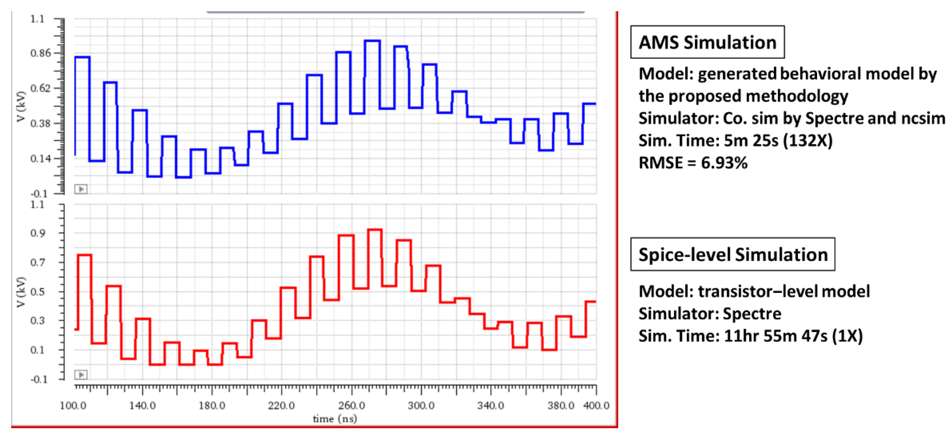
| 246K | <75 s | 00:5:25 (132×) | 11:55:47 (1×) |
| Recognized Digital Blocks | |||
| #RLCD | #TG | #Std Cell | #DCC+current |
| 371 | 45 | 16 | 37 |
| Recognized Analog Blocks | |||
| L1 | L2 | L3 | >L4 |
| 259 | 146 | 39 | 17 |
Publisher’s Note: MDPI stays neutral with regard to jurisdictional claims in published maps and institutional affiliations. |
© 2021 by the authors. Licensee MDPI, Basel, Switzerland. This article is an open access article distributed under the terms and conditions of the Creative Commons Attribution (CC BY) license (https://creativecommons.org/licenses/by/4.0/).
Share and Cite
Song, L.-Y.; Lou, Y.-K.; Lin, C.-H.; Liu, C.-N.; Huang, J.-D.; Jou, J.-Y.; Lee, M.-J.; Lo, Y.-L. Efficient Circuit Structure Analysis for Automatic Behavioral Model Generation in Mixed-Signal System Simulation. Electronics 2021, 10, 1088. https://doi.org/10.3390/electronics10091088
Song L-Y, Lou Y-K, Lin C-H, Liu C-N, Huang J-D, Jou J-Y, Lee M-J, Lo Y-L. Efficient Circuit Structure Analysis for Automatic Behavioral Model Generation in Mixed-Signal System Simulation. Electronics. 2021; 10(9):1088. https://doi.org/10.3390/electronics10091088
Chicago/Turabian StyleSong, Ling-Yen, Yu-Kang Lou, Ching-Ho Lin, Chien-Nan Liu, Juinn-Dar Huang, Jing-Yang Jou, Meng-Jung Lee, and Yu-Lan Lo. 2021. "Efficient Circuit Structure Analysis for Automatic Behavioral Model Generation in Mixed-Signal System Simulation" Electronics 10, no. 9: 1088. https://doi.org/10.3390/electronics10091088
APA StyleSong, L.-Y., Lou, Y.-K., Lin, C.-H., Liu, C.-N., Huang, J.-D., Jou, J.-Y., Lee, M.-J., & Lo, Y.-L. (2021). Efficient Circuit Structure Analysis for Automatic Behavioral Model Generation in Mixed-Signal System Simulation. Electronics, 10(9), 1088. https://doi.org/10.3390/electronics10091088