


Abstract
Some applications such as fuel cells or photovoltaic panels offer low output voltage, and it is essential to boost this voltage before connecting to the grid through an inverter. The Z-network converter can be used for the DC-DC conversion to enhance the output voltage of renewable energy sources. However, boosting capabilities of traditional Z-network boost converters are limited, and the utilization of higher parts count makes it bulky and expensive. In this paper, an efficient, high step-up, switched Z-source DC-DC boost converter (HS-SZC) is presented, which offers a higher boost factor at a smaller duty ratio and avoids the instability due to the saturation of inductors. In the proposed converter, the higher voltage gain is achieved by using one inductor and switch at the back end of the conventional Z-source DC-DC converter (ZSC). The idea is to utilize the output capacitor for filtering and charging and discharging loops. Moreover, the proposed converter offers a wider range of load capacity, thus minimizing the power losses and enhancing efficiency. This study simplifies the structure of conventional Z-source converters through the deployment of fewer components, and hence making it more cost-effective and highly efficient, compared to other DC-DC boost converters. Furthermore, a comparison based on the boosting capability and number of components is provided, and the performance of the proposed design is analyzed with non-ideal elements. Finally, simulation and experimental studies are carried out to evaluate and validate the performance of the proposed converter.
1. Introduction
Renewable energy sources (RESs) are considered as alternatives to conventional fossil fuel-based power generation systems due to several benefits. The solar photovoltaic (PV) system is considered one of the most popular RESs, while hydrogen fuel cells (FCs) are gaining popularity. However, the output voltage generated by both PV units or FCs is lower than the desired voltage level for the integration with the main grid through voltage source inverters [1,2]. One solution for achieving the desired voltage level is to use multiple PV cells or FCs in series in which several cells might be shaded and become reverse biased, i.e., working as a load rather than a source. Furthermore, the power mismatch in PV or FC modules can lead to high power dissipation; hence, the output power decreases [3,4,5]. Therefore, DC-DC boost converters are required to achieve the desired voltage gain so that the voltage level can be increased from the lower value to higher. Theoretically, traditional DC-DC converters offer high voltage gain; however, the performance is not promising in practical applications. For example, converters in refs. [6,7,8] are presented for grid-connected inverter applications. However, the boost factor is lower, which will lead to the utilization of a higher duty cycle; thus, the higher-rated components need to be selected that will increase the cost of the system. Moreover, these converters suffer from large reverse recovery problems [9]. Therefore, the configurations of DC-DC converters play a vital role in the effective integration of RESs.
Numerous voltage-boosting techniques are provided in the existing literature. For example, the voltage lift technique is employed in [10], which increases the boost ability; however, it is not suitable for high power applications. The DC-DC converter in [11] utilizes coupled inductors to enhance the boost capability nevertheless the stress on switches increases due to voltage spikes with a larger amplitude. In ref. [12], switched capacitors-switched inductor cells are used in DC-DC converters to obtain a higher voltage gain. However, the cost of the proposed design increased due to utilization of higher part count that makes the circuit complex and bulky. The DC-DC converter with switched inductors technique is presented in [13] to enhance the boost ability; however, it requires more passive components. Similarly, the voltage multiplier technique is reported in [14] to enhance the voltage gain though it requires several cells with higher ratings. Since all these techniques for DC-DC converters are complex and increase the cost and size of the system, a completely new topology is required to solve these problems.
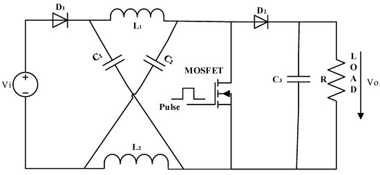
A simple and efficient idea is presented in [15] by proposing a Z-source topology, as shown in Figure 1.
Figure 1.
The traditional Z-source DC-DC converter (ZSC) [5].
The Z-source network in Figure 1 comprises two inductors and capacitors connected in X shape through which the problems of shoot-through and limited voltage gain in traditional voltage DC-DC converters can be resolved to some extent. However, the DC-DC converter with the Z-source network in [15] suffers from the limitation of the lower range of the boost ratio. Recent studies demonstrate that conventional Z-source converters also suffer from few drawbacks, e.g., the high voltage stress on capacitors, discrete input current, large inrush starting current, extreme duty cycle utilization for the high voltage gain, etc. Moreover, it does not provide a common ground for the input and output that results in the higher cost, increased complexity, and larger voltage stress on semiconductor devices [16,17].
Several enhancements are made to Z-source converters in order to solve the problems associated with classical converters in a similar frame. For example, switched inductor-capacitor technology is used in [18,19] to design the Z-source converter. However, the problem still persists as it exhibits a limited voltage gain. Moreover, these topologies have employed a higher number of components that increase the total cost of the system. A high voltage gain is realized in [20,21] by using Z-network based isolated boost converter. Nevertheless, switches experience high voltage spikes due to the coupled inductors in this configuration. In ref. [22], a Z-source DC-DC converter (ZSC) based on the coupled inductor and switched capacitor technique is proposed. The proposed design attains higher gain without utilizing a higher duty cycle. Moreover, the output diode is switched off at zero current, thereby reducing the reverse recovery problem of diodes. However, this design has utilized the higher part count that has made the circuit complex and increased the total cost of the converter. A three-Z-network converter topology is proposed in [23], which has the capability to generate the high voltage gain but at the cost of a large number of passive components and high duty cycles. Similarly, the converter topology as presented in [24,25] utilizes voltage multipliers to increase the boost capability of the converter. However, the switch stress is very high due to high passive components, while showing an increasing trend for other factors, e.g., size, weight, and cost of the converter. Although converters provided in [26,27,28], ensure enhanced gain for the smaller duty cycle, the limitations of high passive components still exist in these converters.
This paper presents a high step-up, switched Z-source converter (HS-SZC) topology to reduce the number of passive components in a circuit while offering a high boost ratio for the smaller duty cycle. The proposed converter topology with a reduced number of components and high gain can be employed in many practical applications, such as DC microgrids, inverters in the two-stage power conversion system, DC motors, electric vehicles, etc. This converter ensures a wider load capacity, which helps to minimize converter losses by utilizing components with lower power ratings, and thus reducing the cost and size of the converter with enhanced efficiency.
The remainder of this paper is arranged as follows. Section 2 defines the circuit configuration and working principle of the proposed HS-SZC. Calculations of the current and voltage stresses on components are defined in Section 3. Section 4 analyzes the components design principle. Section 5 illustrates the impact of non-ideal elements, and the conditions for the continuous conduction mode (CCM) operation are provided in Section 6. The comparison with conventional Z-network converters is presented in Section 7. Finally, simulation and experimental results are discussed in Section 8 and Section 9, respectively, to verify theoretical analysis, while conclusions are drawn in Section 10.
2. Circuit Configuration and Operating Principle of the Proposed HS-SZC
This section illustrates the physical structure and steady-state operational principle of the proposed switched Z-source DC-DC converter.
2.1. The Configuration of the Proposed HS-SZC
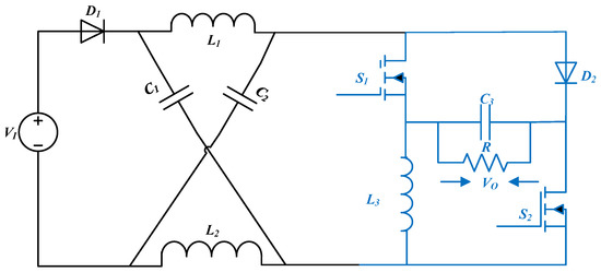
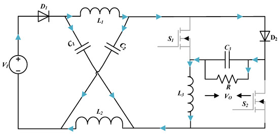
The circuit diagram of the proposed converter is demonstrated in Figure 2, from which it can be observed that it has a very simple structure.
Figure 2.
Configuration of the proposed high step-up, switched Z-source DC-DC boost converter (HS-SZC).
The structure in Figure 2 comprises a Z-source network (L1, C1, L2, and C2), two diodes (D1 and D2), two switches (S1 and S2), an inductor (L3), a filter capacitor (C3), and load resistance (R). Similar to the conventional Z-network converter in Figure 1, the proposed design is composed of an extra switch and inductor (L3) at the backend. The idea is to utilize the output capacitor (C3) and inductor (L3) for filtering and charging and discharging loops so that this helps to increase the voltage gain, which is proved in the following subsection.
2.2. Operating Principle of the HS-SZC
This section outlines the steady-state operating principle for the proposed Z-source DC-DC converter, as shown in Figure 2. The following assumptions are made for the analysis:
- Power components are assumed as ideal without having turn-on resistances and voltage drops;
- Large capacitors are used in order to ignore voltage ripples;
- The proposed converter is operating in the CCM.
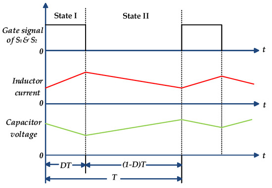
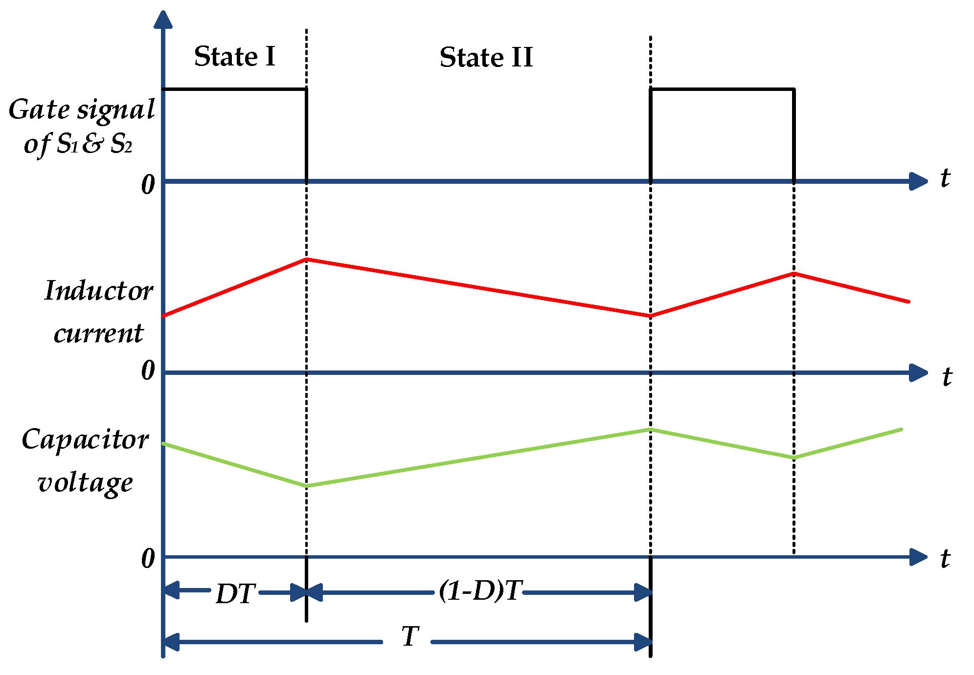
Two switches S1 and S2 within the proposed converter topology are simultaneously turned OFF and ON in order to utilize the same gate pulse. Figure 3 shows the switching states of the proposed converter topology. In this topology, capacitors C1, C2, and C3 discharge energy to inductors L1, L2, and L3 during the ON state of switches, and hence, the current in inductors (L1, L2, and L3) will be increasing (charging). Similarly, inductors L1, L2, and L3 release energy to capacitors C1, C2, and C3, and to loads during the OFF state of switches, and thus, the voltage across capacitors C1, C2, and C3 will start increasing.
Figure 3.
The gating sequence of the HS-SZC.
It is evidenced from Figure 3 that the fundamental operating principle of the proposed HS-SZC is similar to that of a conventional ZSC, in which capacitors discharge energy to inductors in Mode 1 and are charged by inductors and input power supply in Mode 2. [5]. Based on this operating principle, the operational mode of the proposed topology can be classified into two modes, as discussed in the following subsection.
2.2.1. Mode 1
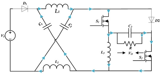
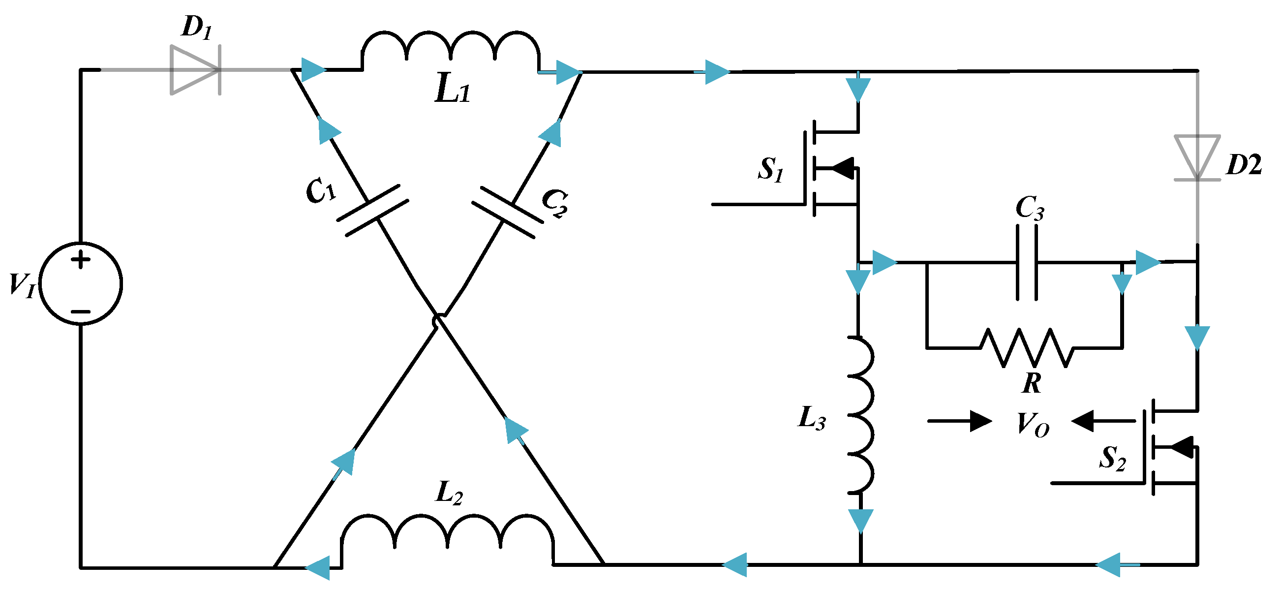
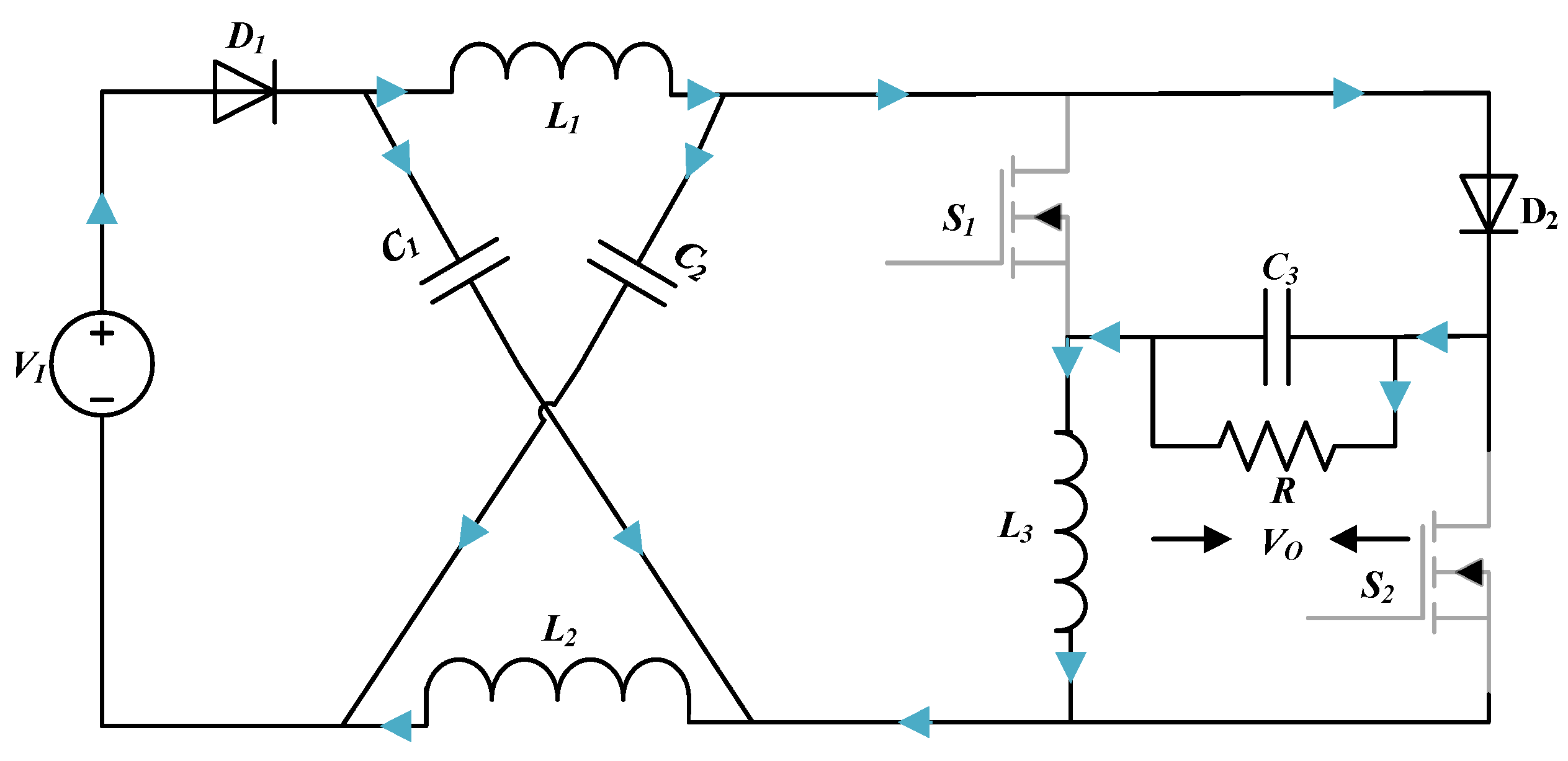
The equivalent circuit of the proposed HS-SZC in Mode 1 is shown in Figure 4.
Figure 4.
The configuration of the proposed HS-SZC during operating in Mode 1.
In this mode, both switches will be turned ON and diodes will be reverse biased. In this condition, L1 will be charged by C1 and C3; L2 will be charged by C2 and C3; L3 will be charged by C2 and C3; and load will be supplied by the parallel output capacitor (C3). Referring to the current direction in Figure 4, the inductor L1 has the same current as of the capacitor C1 (i.e., IC1 = IL1, where IC1 is the current flowing through C1, and IL1 is the current flowing through L1); the capacitor C2 has the equal current as of the inductor L2 (i.e., IL2 = IC2, where IC2 is the current flowing through C2, and IL2 is the current flowing through L2). Similarly, the currents through switch S1 and switch S2 are the same (i.e., IS1 = IS2, where IS1 is the current flowing through S1 and IS2 is the current flowing through S2). According to Kirchhoff’s voltage (KVL) and current laws (KCL), the following equations can be obtained:
where VL1 and VL2 are voltages across L1 and L2, respectively; VC1, VC2, and VC3 are voltages across C1, C2, and C3, respectively; VO is the voltage across the load: IL3 and IC3 are currents through L3 and C3, respectively; and IO is the current through the load.
2.2.2. Mode 2
The equivalent circuit of the proposed HS-SZC operating in Mode 2 is shown in Figure 5.
Figure 5.
The configuration of the proposed HS-SZC during operating in Mode 2.
In this mode, both switches will be turned OFF and diodes will be forward-biased. Under this condition, the input voltage (VI) including L1 and L2 discharge energy to both capacitors C1 and C2, respectively. Here, C3 is charged by all inductors and VI, which is also supplied to the load. Referring to the current direction in Figure 5, diodes D1 and D2 have the same amount of current. According to Kirchhoff’s voltage (KVL) and current laws (KCL), the following equations can be obtained:
where VL3 is the voltages across L3. In order to work under steady-state conditions, the inductor needs to follow the volt-sec principle. The volt-sec principle refers to the fact that the sum of volt-seconds applied to an inductor during on and off time must be zero. The volt-sec is defined as (), which states that the change in the current (di) is proportional to the product of voltages (volts) and time (seconds). Using the volt-sec principle for inductors in both states and solving relevant equations, it can be written as
where G and D are defined as gain factor and duty cycle, respectively. Apart from these two modes, the proposed converter can go to the transient mode. In this case, switches will experience higher voltage spikes; thus, more power losses will occur. In general, in order to avoid this situation snubber circuits are utilized as discussed in [29]. Moreover, from Equation (15), it is worth noting that the boost ability of the proposed switched converter is (3 − 4D) / (1 − 3D), which is higher than other converters presented in literature. From Equation (14), it can be observed that the value of D should not exceed 0.33 in order to avoid instability due to the saturation of inductors and singularity problems. The detailed calculations of current stresses on components are discussed in the following section.
3. Calculation of Current Stresses
For an ideal condition, the input and output power for the proposed HS-SZC can be specified as
which can be written as
where II is the input current. Under this condition, the average input current can be obtained as
Since,
therefore,
From Figure 2, the input voltage VI has a series connection with diode D1, i.e., (II = ID1), where ID1 is the current flowing through D1. Therefore, the input current can also be written as
Since, II = ID1, putting the value of II in Equation (20), it can be written as
Further simplifying and considering the current Equations in Mode 2, the following Equation can be obtained:
Using the Equations (1)–(12), the current stress on components can be derived as follows:
The current stress on D1 is
The current stress on D2 is
The current stresses on S1 and S2 are
Table 1 list the voltage and current stress on each component.
Table 1.
Current and voltage parameters of the HS-SZC.
4. Component Design Principle
The component design is generally dependent on current and voltage stresses, which are provided in Table 1. In this section, the analysis of the component design principle for the proposed HS-SZC is described in detail.
4.1. Inductor Design
The following equation can be used to determine the inductor:
By considering the inductor during the operational Mode 1, Equation (27) can be written as
It can be further simplified as
Substituting Equation (1) into Equation (29) and further simplifying the equation, it can be obtained as
where ΔIL and fS denote the inductor current ripple and switching frequency, respectively. Subsequently, a larger current ripple will produce higher current stresses on diodes and switches; therefore, this value should be minimized. Normally, the current ripple is described as
where XL% is the percentage inductor current ripple. Using Equation (30) into Equation (31) and assuming XL% as the maximum current ripple of the inductor in Mode 1, it can be written as
Finally, Equation (32) can be used to determine the inductors (L1, L2, and L3) for the proposed topology.
4.2. Capacitor Design
The following equation can be used to determine the capacitor:
By considering the capacitor during the operational in Mode 1, Equation (33) can be written as
That can be further simplified as
Since the capacitor current IC equals to the inductor current IL during the switch-on period, the substitution of the value of IL into Equation (35) will result in
where ΔVC the capacitor voltage ripple. The larger voltage ripple will reduce the lifetime of the capacitor and it will also require a higher value of the capacitor. Therefore, this value should be minimized for which the capacitor voltage ripple can be described as
where XC% is the percentage capacitor voltage ripple. Using Equation (36) into Equation (37) and assuming Xc% as the maximum voltage ripple of the capacitor in Mode 1, it can be written as
Finally, Equation (38) can be used to determine the capacitors (C1, C2, and C3) for the proposed topology.
4.3. Switch and Diode Design
The choice of switches and diodes is fully dependent on their voltage and current stresses. For the proposed HS-SZC, the voltage and current stresses are provided in Table 1. It is observed from Table 1 that the voltage stress on the switches is equivalent to the output voltage, whereas the current stress will vary according to the value of the duty cycle. For instance, if D = 0.15, the current stress will be equivalent to 1.96IO. Therefore, the values of output voltage and current must be considered, in order to decide the ratings of switches and diodes.
5. Analysis of the Proposed HS-SZC with Non-Ideal Elements
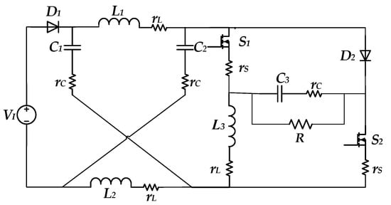
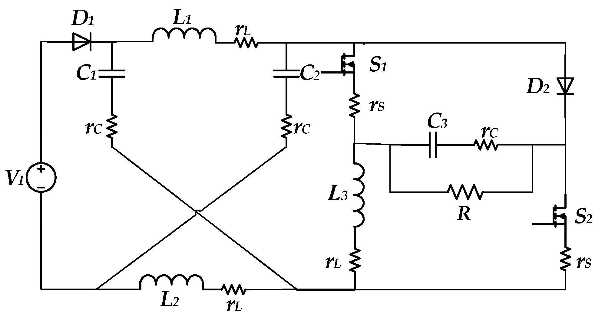
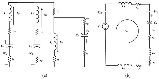
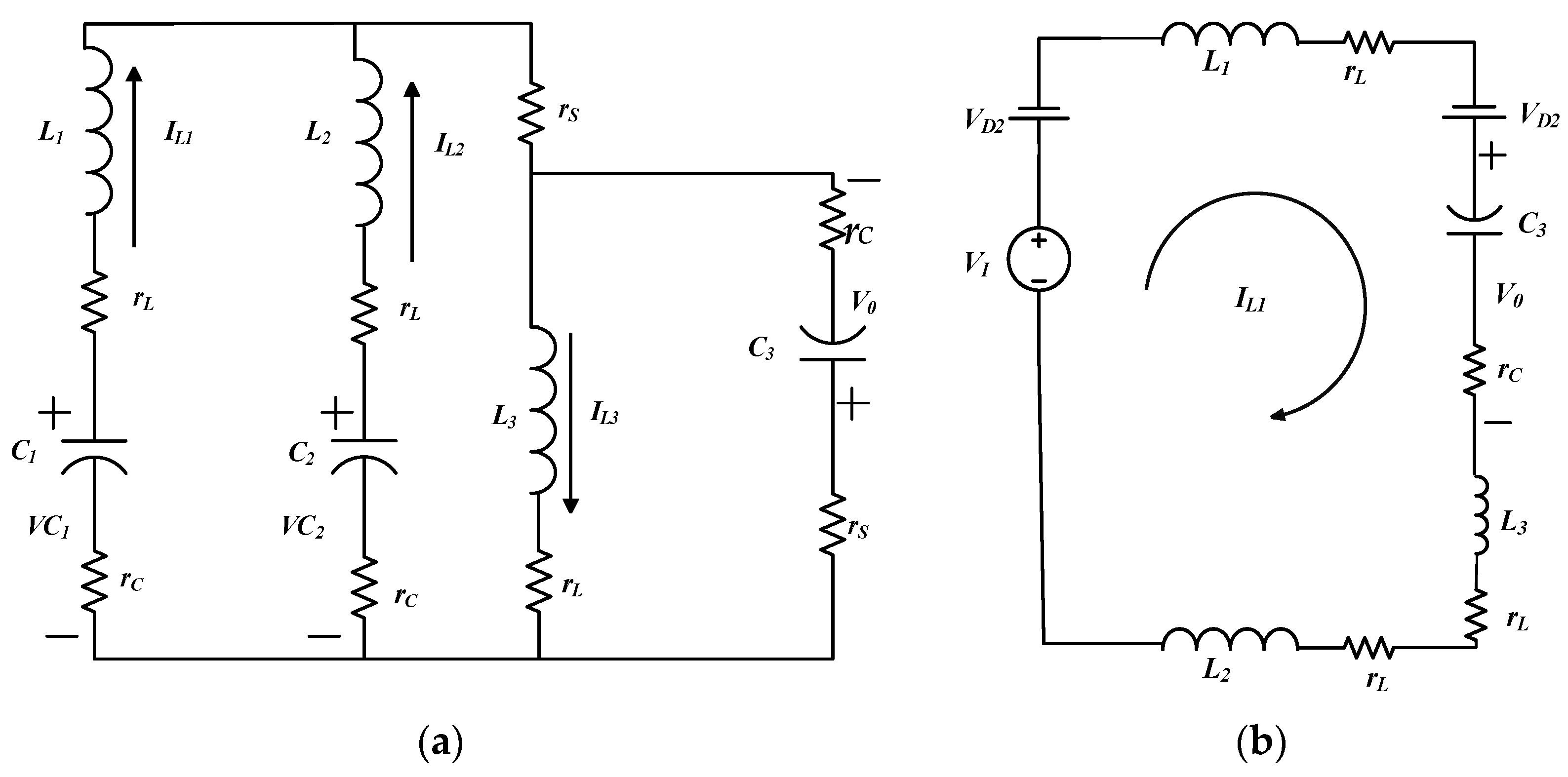
The impact of parasitic parameters on the proposed converter is studied in this section along with the calculations of the output voltage and efficiency. Parasitic parameters are undesirable circuit elements possessed by electronic components, which are also known as internal parameters. Figure 6 and Figure 7 show the proposed converter with internal parameters and current loops for both operating modes, i.e., for Mode 1 and Mode 2, respectively.
Figure 6.
The circuit diagram of the proposed converter with non-ideal elements.
Figure 7.
The equivalent current loops with non-ideal elements: (a) Mode 1 and (b) Mode 2.
Parasitic parameters involve ON resistance (rS) of both switches, series resistance (rC) of capacitors, inductor’s winding resistance (rL), and voltage drop for the diode (VD). It is worth noting that the ripples in the capacitor voltage and inductor current are not considered during the analysis as presented in this section. The impact of these non-ideal elements or parasitic parameters is analyzed based on the output voltage and efficiency, as discussed in the following subsections.
5.1. Impact of Non-Ideal Elements on the Output Voltage
The ideal output voltage equation for the proposed converter is given in Equation (13). However, it is essential to analyze the impact of parasitic parameters and the voltage drop across semiconductor devices, which need to be considered during the practical operation, and hence, the actual value of the output voltage will not be the same. Assuming each inductor has an average value of current IL, the actual output voltage can be specified as
From Equation (39), it can be observed that the difference between ideal and actual voltage does not depend on the input voltage. The impact of parasitic parameters is analyzed by considering the parameters of the proposed converter, as shown in Table 2.
Table 2.
Non-ideal components.
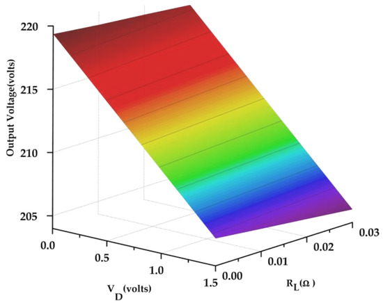
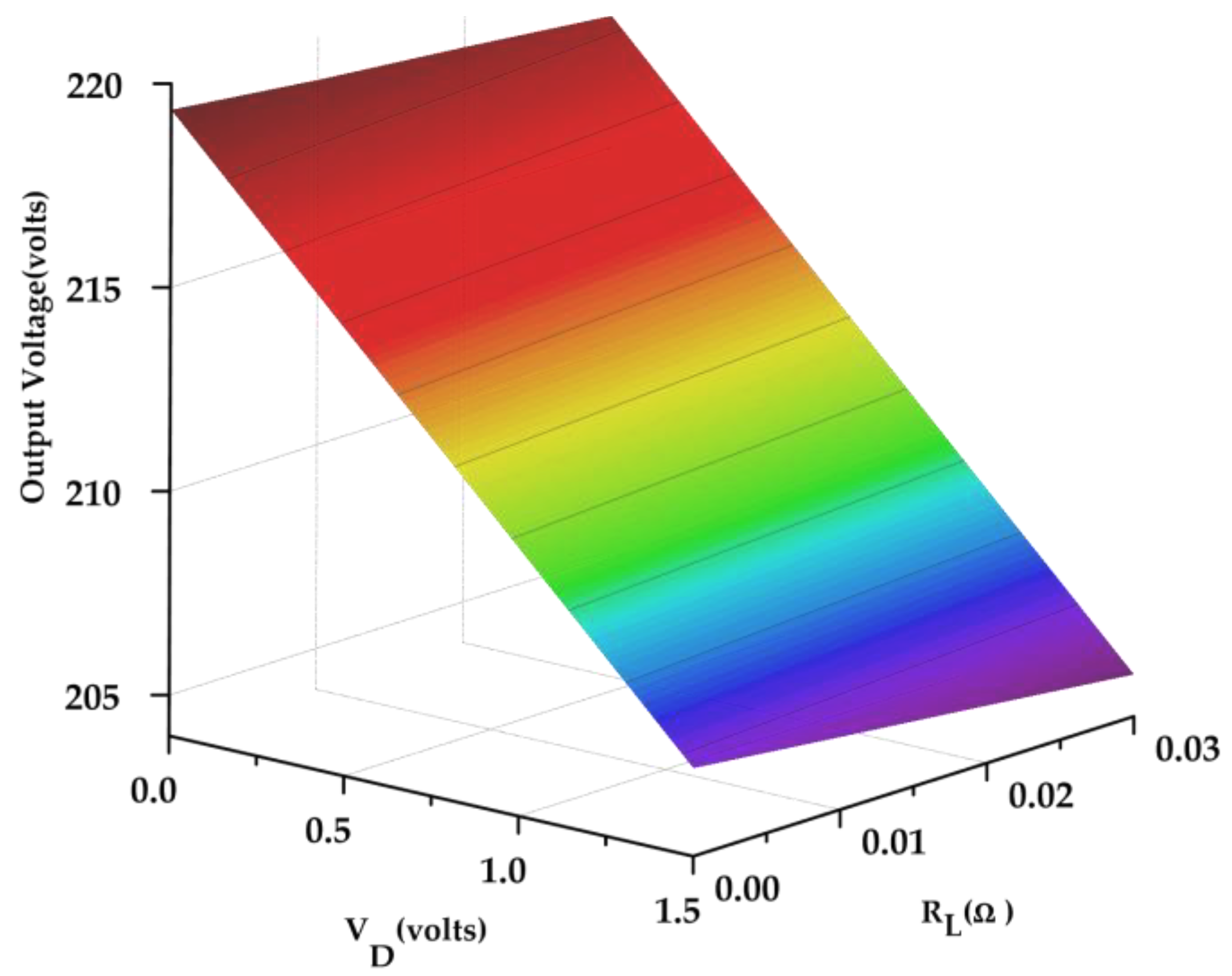
This subsection analyzes the impact of non-ideal elements on the output voltage of the proposed converter by varying the values of VD and rL. From this analysis, it can be realized that the proposed converter achieves an ideal gain of more than five times of input voltage VI for the duty cycle, D = 0.20. However, considering the parasitic parameters in Table 2, this value will be decreased.
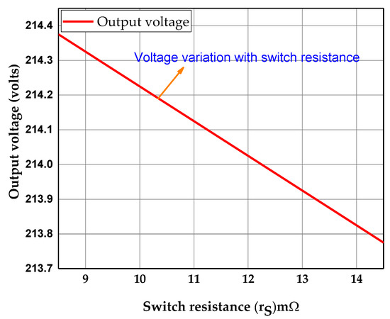
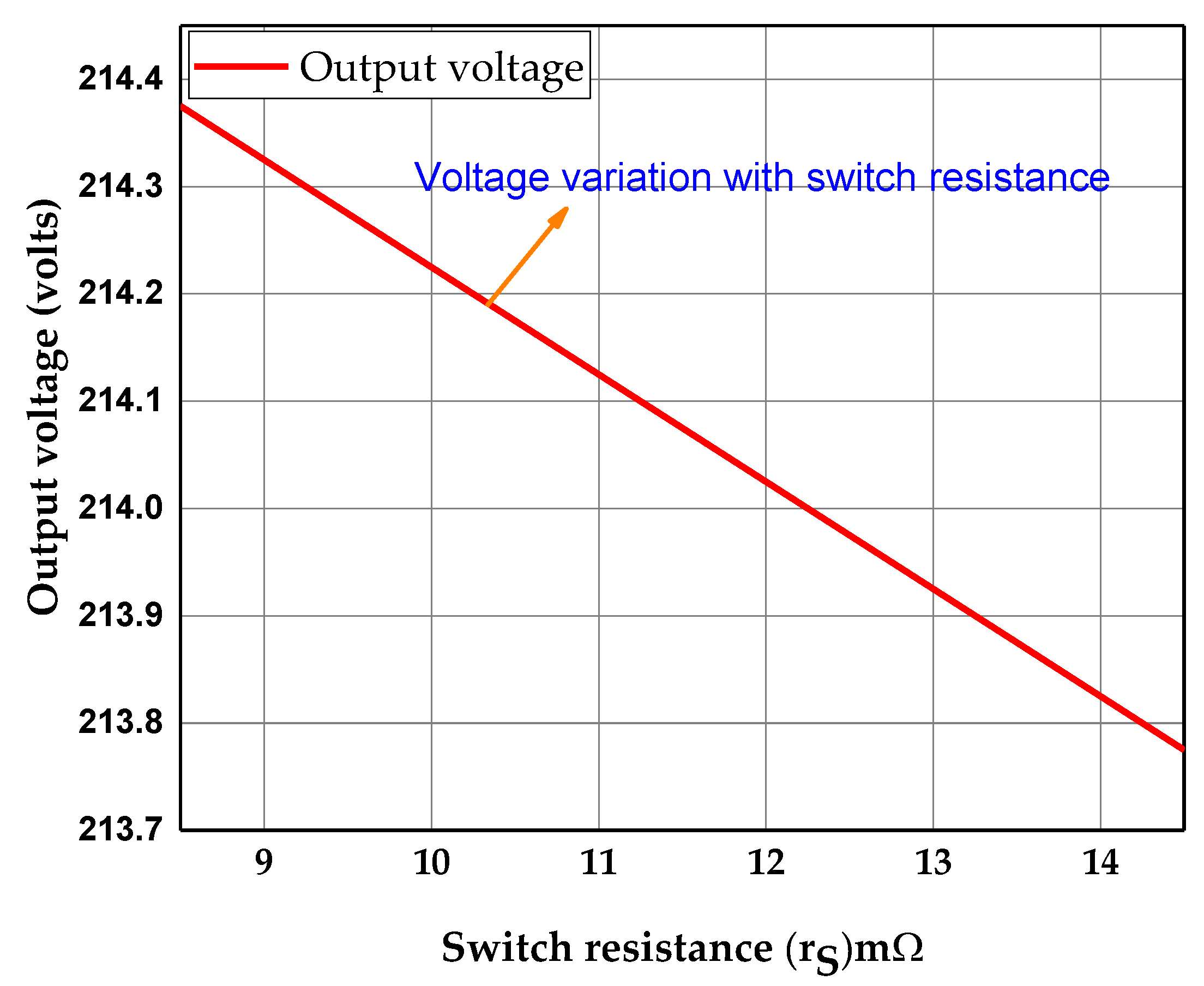
Referring to Figure 8, the difference between actual and ideal voltage is that the actual one is inversely proportional to the values of VD and rL. Thus, the smaller the values of VD and rL, the closer the value of the actual output voltage to the ideal voltage. In a real-world application, switches are not ideal. There are some internal resistances to the power path which directly affects the performance of the converter. Therefore, a higher value of resistance will result in a higher voltage drop, increased power dissipation, and higher power loss. Figure 9 demonstrates the variation of the output voltage with the switch resistance rS, in which the lower values of the resistance ensure the higher output voltage. In addition, faster switching is necessary for the converters because it leads to select power components with lower ratings, thus decreasing the cost of the converter. Therefore, these parameters must be kept into consideration for designing simulations and experimental prototypes.
Figure 8.
Variation in the theoretical output voltage with changes in VD and rL.
Figure 9.
Variation in the theoretical output voltage with changes in rS.
5.2. Impact of Non-Ideal Elements on the Efficiency
The efficiency calculation for the DC-DC converter is entirely dependent on losses that occur in the converter. The converter losses include conduction and parasitic parameter losses. In this section, to determine the efficiency, the following converter losses are determined for the proposed HS-SZC.
5.2.1. Power Losses in the Switch
The power loss in the switch comprises conduction loss and switching loss. The conduction loss depends on the root mean square (r.m.s) value of the switch current and turn-on resistance of switches. However, switching losses occur due to the turn-off and turn-on delay of switches. The conduction loss (PC-SWITCH) can be determined by using the following equation:
where the r.m.s value of the switch current (Ir.m.s) can be written as
Furthermore,
Substituting Equation (42) into Equation (41), it can be written as
Substituting Equation (43) into Equation (40), the total conduction loss in the switch can be expressed as
Moreover, it can be assumed for switching losses assuming that the linear voltages are applied across the switches and the linear currents flow through switches during turn-on and turn-off periods. Thus, switching losses for the proposed switched converter can be specified as [30,31]
where ton and toff indicate turn-on and turn-off times, respectively.
5.2.2. Power Losses in the Diode
The diode power loss comprises conduction and reverse recovery losses. The conduction loss depends on the forward voltage drop and the average current flowing through the diode. The conduction loss (PC-DIODE) can be determined by using the following equation:
where the r.m.s value (IDrms) of the diode current (ID) can be written as
Furthermore,
Substituting Equation (48) into Equation (47), it can be written as
Substituting Equation (49) into Equation (46), total conduction loss in the diode can be expressed as
Furthermore, the diode reverse recovery loss can be estimated as
where QRR1, QRR2, and QRR3 are the reverse recovery charges for D1, D2, and D3, respectively.
5.2.3. Power Losses in the Inductor
The inductor power loss is divided into the core loss and conduction loss (i.e., winding loss). For the pulse width modulator (PWM) converter, core losses are very small and can be avoided, although the conduction loss depends on the rms value of the inductor current (IL(r.m.s)) and resistance of inductors rL. The value of IL(r.m.s) can be expressed as
Using Equation (52) and doing some simplifications, the total inductor conduction loss (PC-INDUCTOR) for the proposed switched converter can be obtained as
5.2.4. Power Losses in the Capacitor
The conduction loss in the capacitor depends on the rms value of the capacitor current (IC(r.m.s)) and value of rC, Therefore, for the proposed converter it can be determined by using the following equations:
where the value of IC(r.m.s) can be written as
Substituting Equation (55) into Equation (54) and doing some simplifications, the capacitor conduction loss for the proposed switched converter can be obtained as
5.2.5. Total Power Losses
Generally, the total conduction loss is calculated as
The substitution of Equations (44), (50), (53) and (56) into Equation (57) will result in
Based on Equations (45), (51) and (58), the efficiency of the proposed converter can be determined as
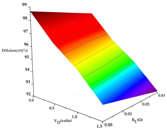
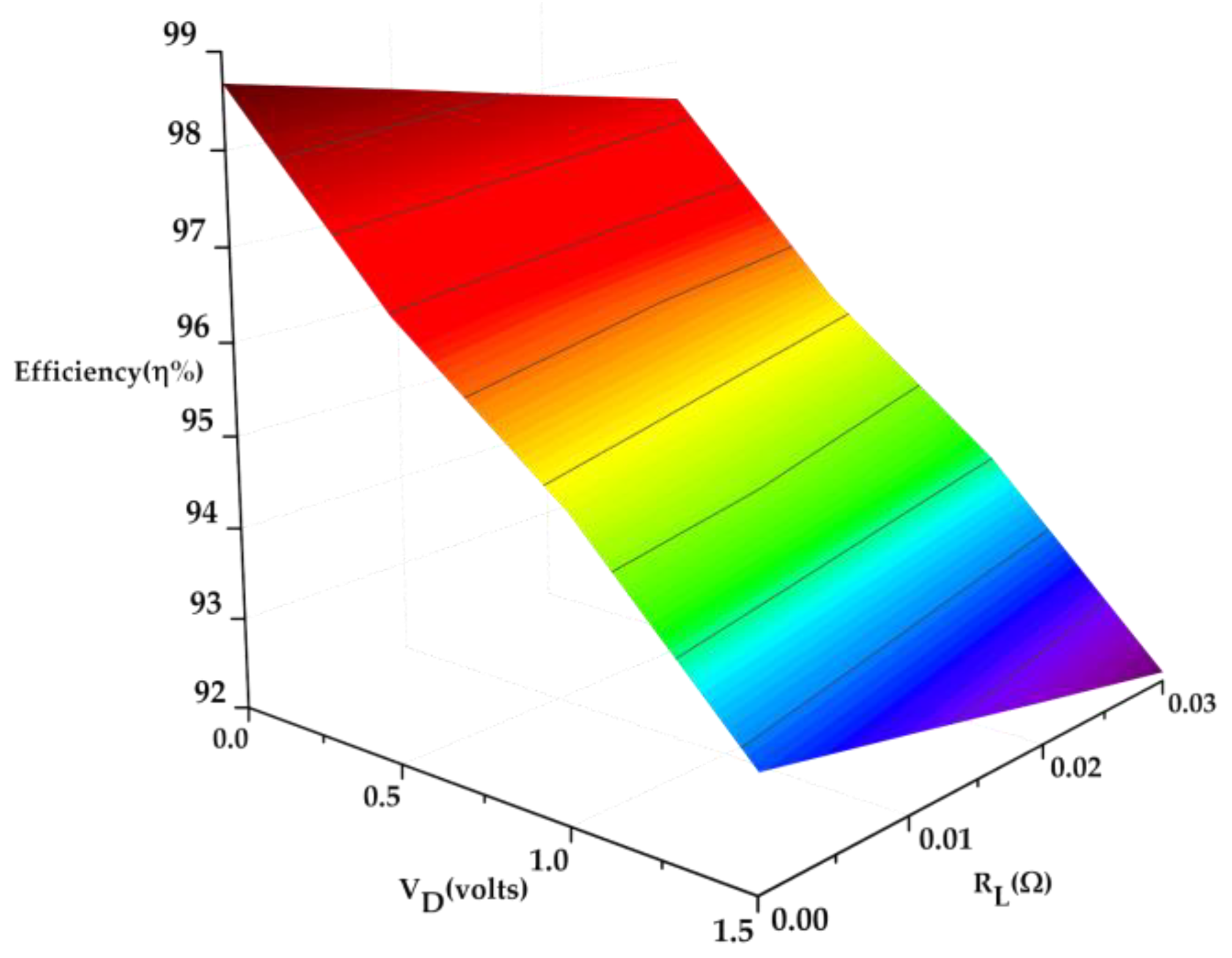
where POUT and PI are output and input power of the proposed converter, respectively. The impact of non-ideal elements on the efficiency of the proposed converter is analyzed by varying the values of rL and VD, including the variation in the switch resistance (rS). Furthermore, a surface, as shown in Figure 10, has been drawn, adopting the parameters used in Table 2 to determine the effects of non-ideal elements on efficiency.
Figure 10.
Variation in the theoretical efficiency with changes in rL and VD.
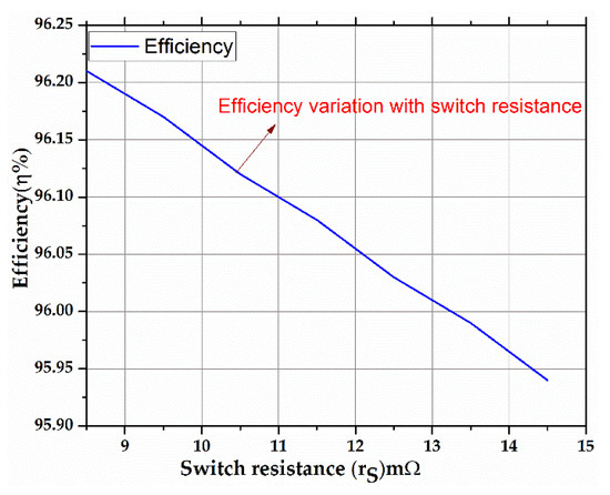
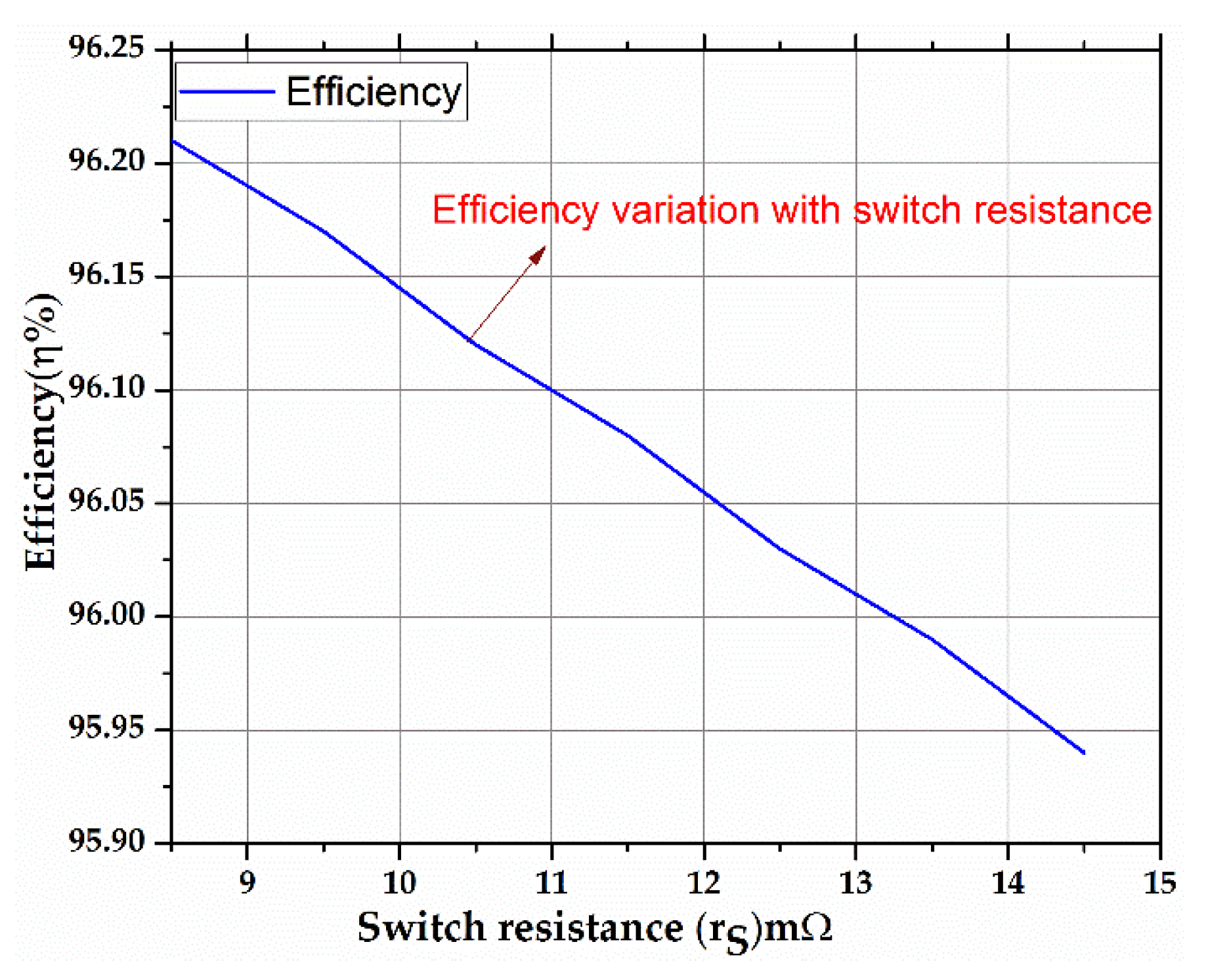
From this analysis, it can be realized that the proposed converter achieves more than 98% efficiency during an ideal condition. However, considering the parasitic parameters in Table 2, this value will be decreased. Figure 11 also shows the variation in the efficiency with the switch resistance, which indicates that the smaller value of the switch resistance will ensure higher efficiency. Therefore, these parasitic parameters have a significant effect on the efficiency of the converter and there will be higher efficiency of the proposed converter if these values are decreased.
Figure 11.
Variation in the theoretical efficiency with changes in rS.
6. Conditions for the CCM Operation and Load Range of the Proposed Converter
The CCM refers to the value of the inductor current not reaching zero in each state. This section demonstrates the conditions for the CCM operation and compares the load ranges for the proposed switched converter with a conventional Z-source DC-DC converter. For the appropriate CCM operation, the proposed converter must satisfy the following condition:
For the switched converter (assuming the input power is equal to output power), it can be written as
which can be written as
Using the Equations (61) and (62), the inductor current can be written as
Subsequently, the larger current ripples will generate higher current stresses on diodes and switches.
Using the Equations (60), (63) and (32); the load range in the CCM operation can be written as
where RL denotes the load resistance. It is clear from Equation (64) that RL is proportional to L. Hence, increases in L will enhance the load capacity of the converter. Moreover, the following condition must be satisfied for the CCM operation of the proposed converter:
where RLmax indicates the maximum load at a specific duty cycle. If the above condition is not satisfied the converter will shift to the DCM operation. For comparing the load capacity with the traditional Z-network converter, it can be written as follows [32]:
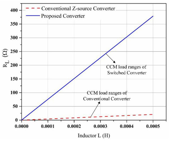
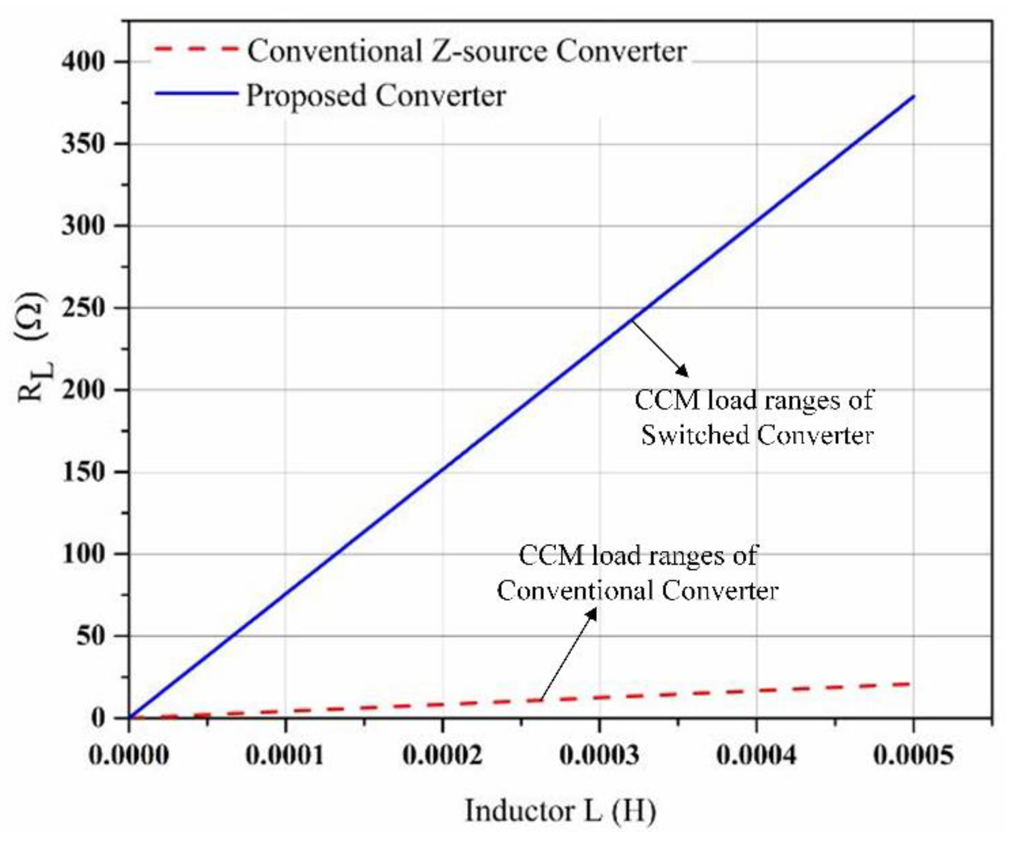
It is worth noting that for the purpose of comparison, it is assumed that both converters are working in the CCM for the specified parameters. Moreover, based on Equations (64) and (6), setting D = 0.20 and fS = 25 kHz the load range of both proposed and traditional converters while working in CCM is shown in Figure 12, from which it can be clearly observed that the proposed converter holds a much wider range, compared to a traditional DC-DC converter having a similar value of the inductor.
Figure 12.
Load range for the proposed converter and traditional Z-source converter.
7. Comparative Analysis of the Proposed Converter
In this section, a comprehensive comparison is presented based on the number of components and boost ability in order to highlight the features of the proposed converter, compared to existing converters. Hence, the comparative study is presented in terms of the boost ability and number of components as discussed in the following subsections.
7.1. Comparison in Terms of the Boost Ability
As discussed earlier, the boost ability is one of the most significant properties for evaluating the performance of a DC-DC converter. In this subsection, the proposed Z-source converter is compared with other Z- source DC-DC converters presented in [15,26,27,28] and [33,34,35,36,37]. The voltage gains of converters in [15,26,27,28] and [33,34,35,36,37] are listed in Table 3.
Table 3.
Performance comparison of the proposed converter and existing converters.
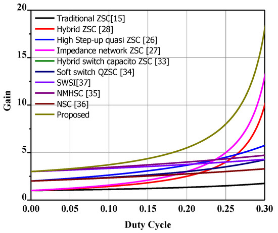
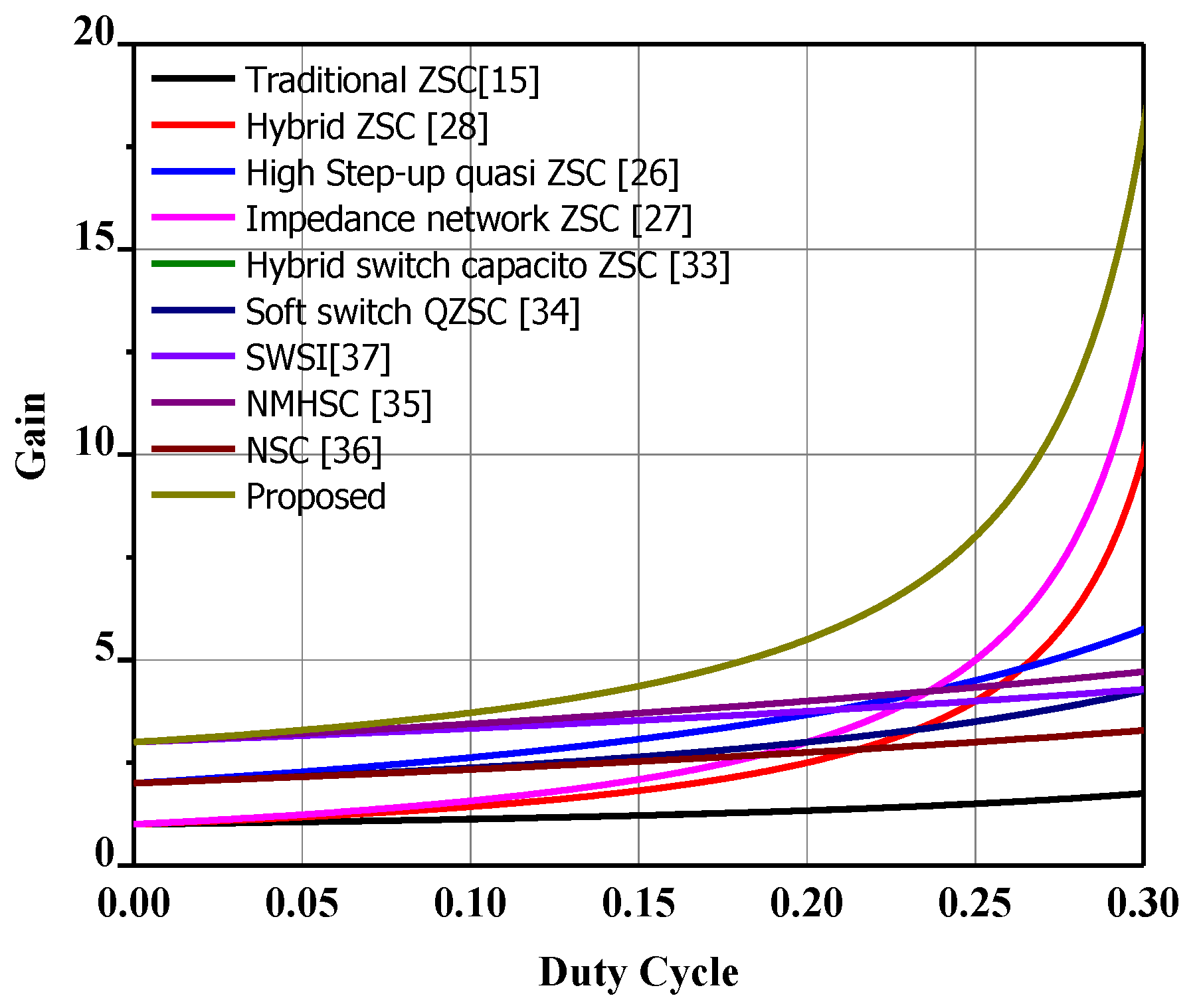
To demonstrate the boost ability of the proposed converter further, the relationship between the boost factor and duty cycle is shown in Figure 13 from which it can be seen that the proposed converter exhibits higher boost ability as compared to all other Z-source converters in a similar frame. It is worth noting that the range of duty cycle is selected from 0–0.30 only for the purpose of comparisons. However, the maximum operating duty cycle for the converters in [15,26,27,28], and is D < 0.5, D < 0.5, D < 0.33, and D < 0.33, respectively; and that of for the converters in [33,34,35,36,37] is D < 1, D < 0.5, D < 1, D < 1 and D < 1, respectively. The maximum operating duty cycle for the proposed converter is D < 0.33.
Figure 13.
Comparison of the boost ability for the proposed and conventional converters.
7.2. Comparison in Terms of the Number of Components
This subsection compares the number of components for the proposed Z-network and other converters presented in [15,26,27,28] and [34,35,36,37]. Table 3 lists the number of components utilized in these converters. The proposed converter utilizes one additional switch and inductor at the backend of the conventional Z-network converter in order to realize a higher boost ratio. From Table 3, it is observed that the proposed converter uses a minimal number of components, compared to other converters, which reduce the cost and size while enhancing the efficiency; the following section presents rigorous simulation and experimental results to analyze the performance of the proposed HS-SZC.
7.3. Comparison in Terms of Voltage Stress
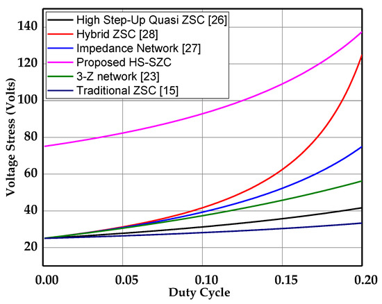
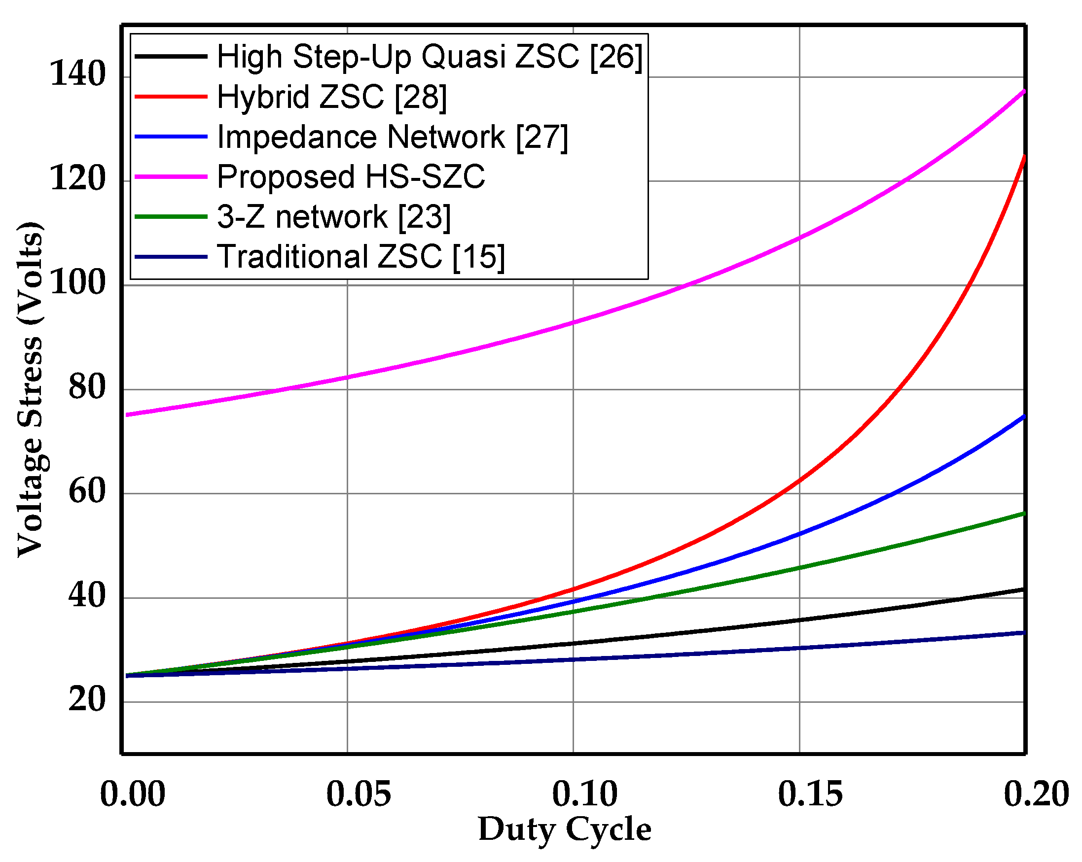
In this subsection, comparisons are presented based on the voltage across switches for conventional converters in [15,23] and [26,27,28] against the proposed converter. The comparative results for VI = 25 V are shown in Figure 14. It is worth noting that apart from the converter in [26], the voltage stress across the switch for other converters is equal to the output voltage at a specific duty cycle. For instance, at D = 0.15, the value of voltage stress for the proposed converter is 109 V; correspondingly, the value of output voltage for the proposed converter at D = 0.15 and VI = 25 V in Figure 13 will be the same. Thus, the proposed converter maintains the features of a traditional ZSC.
Figure 14.
Comparison of the voltage stress for the conventional and proposed converter at the input voltage of VI = 25 V.
8. Simulation Results
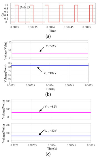
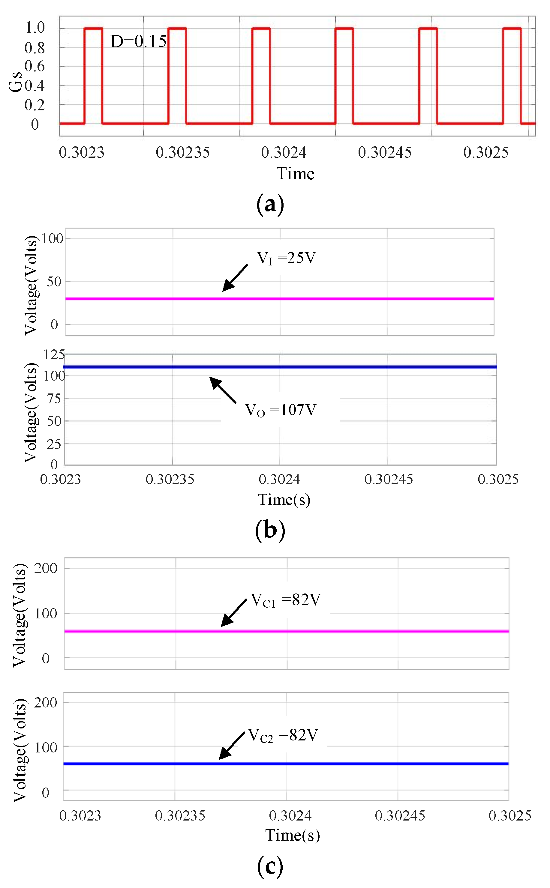
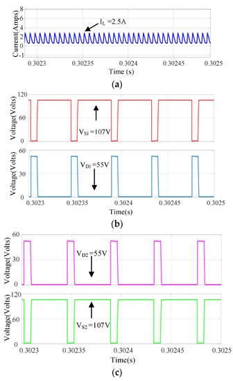
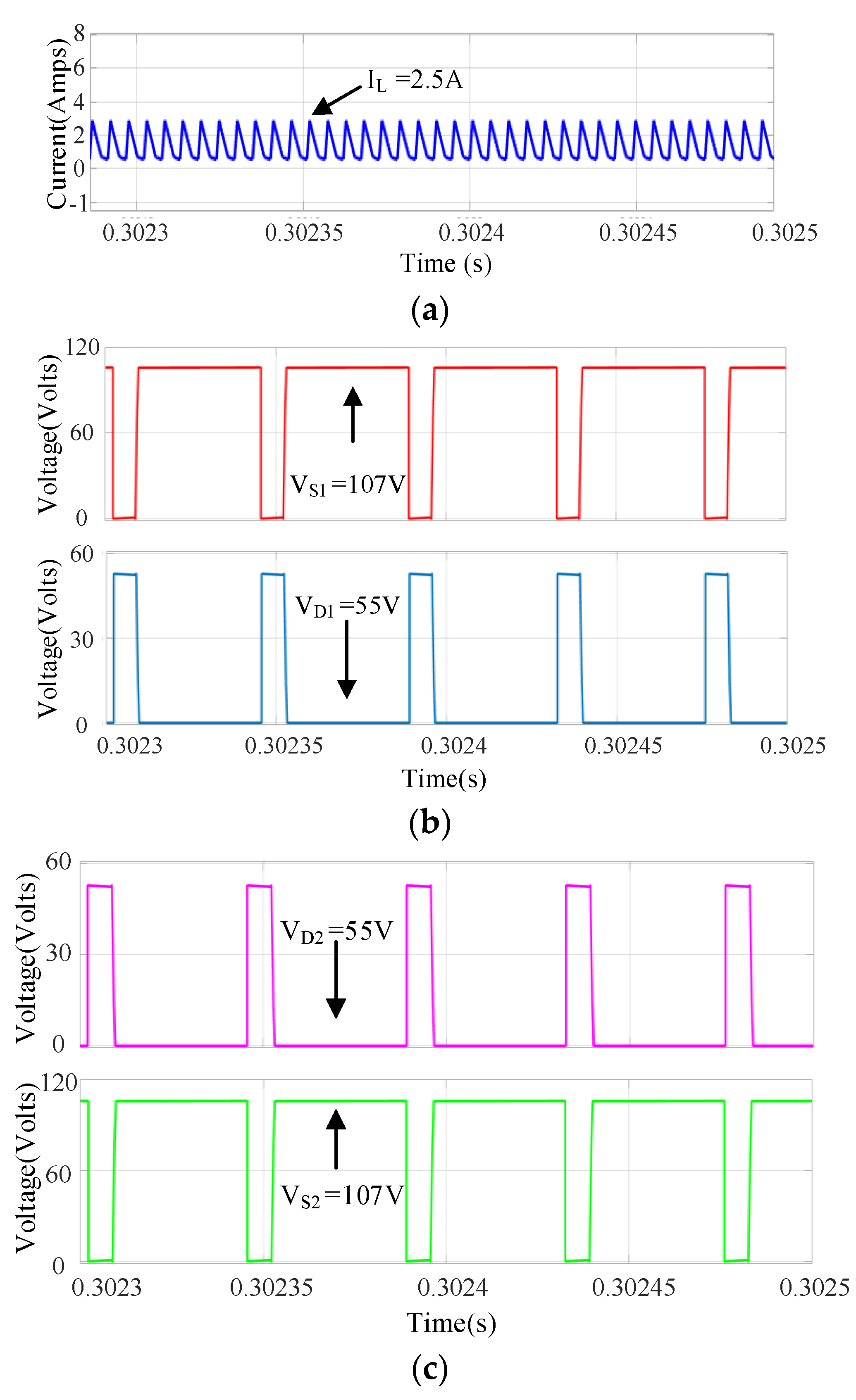
The simulation model for the proposed converter is developed in MATLAB/Simulink environment with specifications of 25/107, 52 W to validate the theoretical analysis. The parameters listed in Table 4 are used for simulations. The key waveforms of the simulated converter such as the gate signal, input voltage, output voltage, voltages across switch S1 and S2, inductor current, and voltages of capacitors C1 and C2 are manifested in Figure 15 and Figure 16. Figure 15a shows the gate signal for both MOSFETs (Metal Oxide Semiconductor Field Effect Transistors) in which the lower duty ratio (D = 0.15) is adopted that minimizes switching losses and enhances the efficiency. Based on Equation (14), the boost factor of the proposed design can be calculated as 4.36 for D = 0.15. Thus, the simulated values of the input and output voltages in Figure 15b are 25 V and 107 V, respectively, which further authenticate the theoretical analysis. As per Equation (13), the theoretical values of voltages across the capacitors C1 and C2 will be the same and this will be 84 V for both capacitors and the simulation results in Figure 15c shows this as 82 V. Hence, theoretical and simulation results match with each other. Moreover, Figure 16 shows the simulated value of inductor current and voltages for both MOSFETs and diodes that are 107 V and 55 V, respectively; hence, simulation results fit with theoretical analysis, which demonstrates the accuracy of the proposed converter.
Table 4.
Simulations and experimental parameters.
Figure 15.
(a) Gate signals, (b) input and output voltages, and (c) voltages across capacitors C1 and C2.
Figure 16.
(a) Inductor current IL, (b) voltage across D1 and S1, and (c) voltage across D2 and S2.
9. Experimental Results
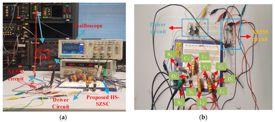
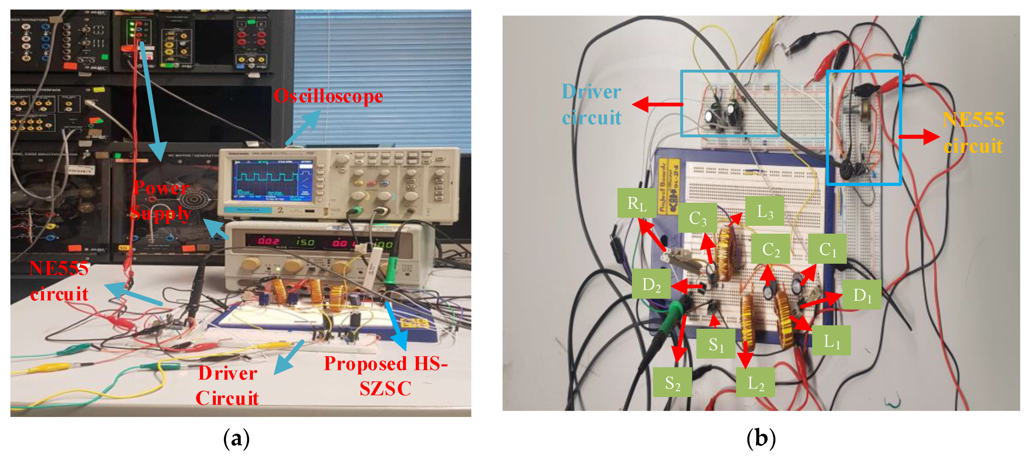
In order to verify the feasibility of the proposed HS-SZC, a prototype is developed and tested in the laboratory. The circuit design and the complete experimental setup are shown in Figure 17. Moreover, the experimental parameters and specifications of devices are presented in Table 4 and Table 5.
Figure 17.
(a) Complete experimental setup and (b) circuit design of proposed HS-SZC.
Table 5.
Specification of experimental devices.
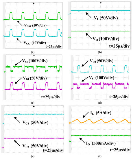
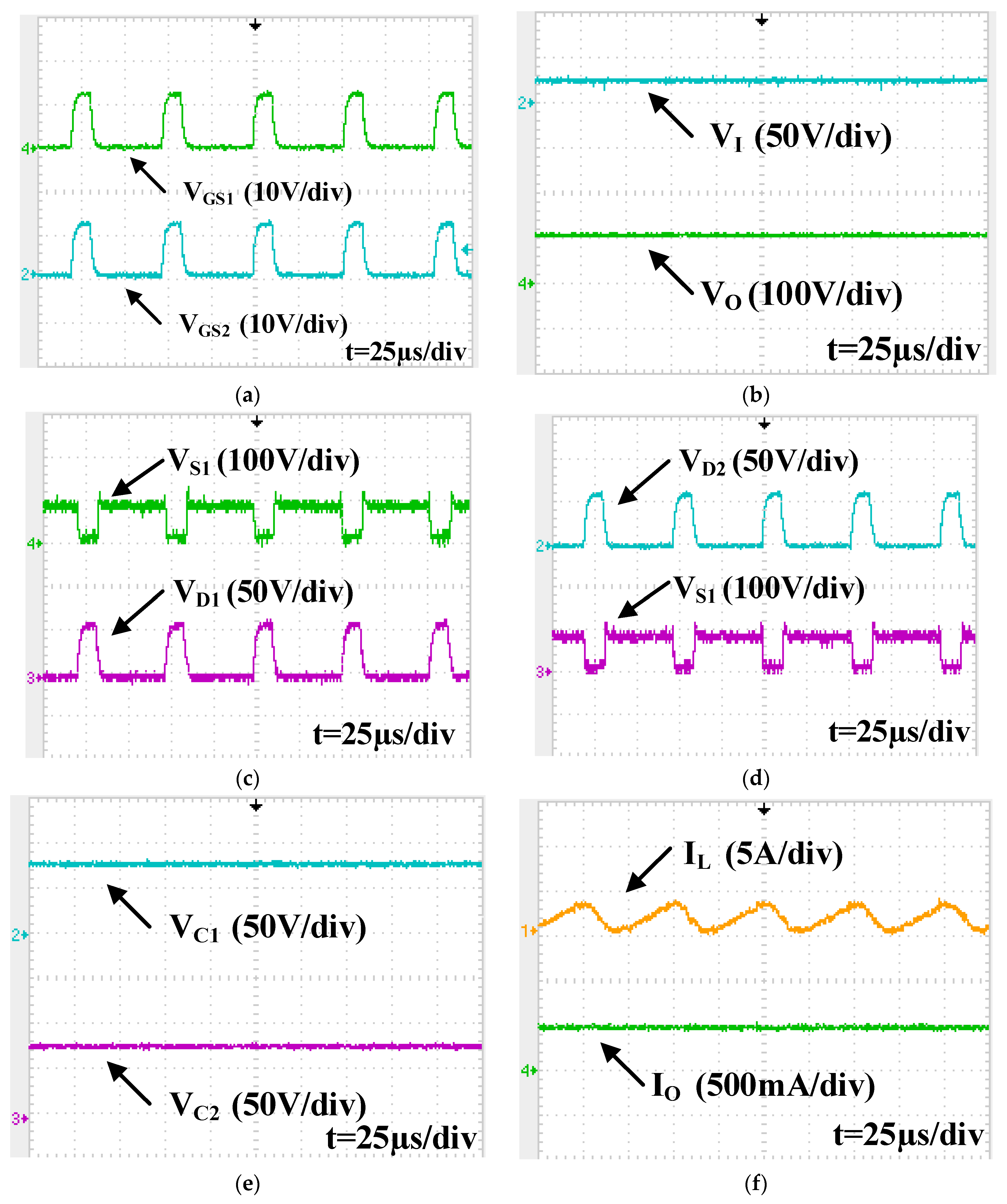
The gate pulses for both MOSFETs (S1 and S2) are generated using a NE555 timer IC with the proper switching frequency and duty cycle. The gate pulses for both switches are shown in Figure 18a, from which it can be observed that the gate signals (VGS1 and VGS2) are operating at the frequency and duty cycle of fS = 20 kHz and D = 0.15, respectively. The theoretical value of the output voltage of the proposed converter at a specified duty cycle and input voltage (D = 0.15, VI = 25 V) is VO = 109 V, for which the gain factor is calculated as 4.36. Correspondingly, the experimental value of the output voltage shown in Figure 18b is 103 V, for which the gain factor becomes 4.12. However, there is a discrepancy of 6 V when compared to the theoretical value. This is in accordance with the graph shown in Figure 8. Thus, the experimental results match well with the theoretical analysis.
Figure 18.
(a) Gate signals for both MOSFETs S1 and S2, (b) input and output voltages, (c) voltages across switch S1 and diode D1, (d) voltages across switch S2 and diode D2, (e) voltages across both capacitors C1 and C2, and (f) inductor current and output current.
The voltage stress waveforms for diodes (D1 and D2) and switches (S1 and S2) are presented in Figure 18c,d, respectively. It is worth noting that the switches (S1 and S2) have a peak value of 103 V which is equivalent to the output voltage; thus, the proposed converter carries the features of the traditional converter. However, the diodes (D1 and D2) have a reduced voltage stress of 51 V, which is much lower than the output voltage. This is one of the key benefits of the proposed converter. The experimental waveforms for voltages across the capacitors (C1 and C2) are shown in Figure 18e and the inductor currents along with the output current waveforms are shown in Figure 18f. Based on Equation (13), the theoretical value of the voltage across both capacitors (C1 and C2) is 84 V, respectively. However, the experimental value of the voltage across both capacitors is 80 V. Therefore, the theoretical analysis is in good agreement with experimental results, which further validates the performance of the proposed converter.
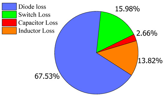
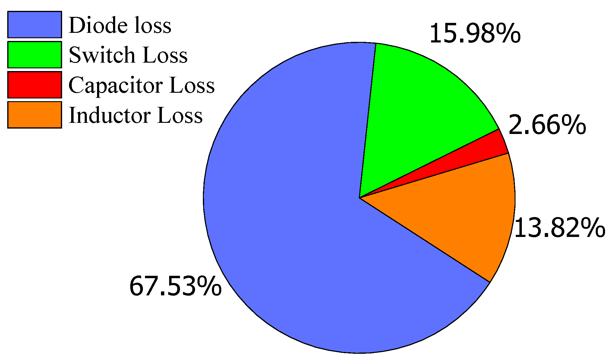
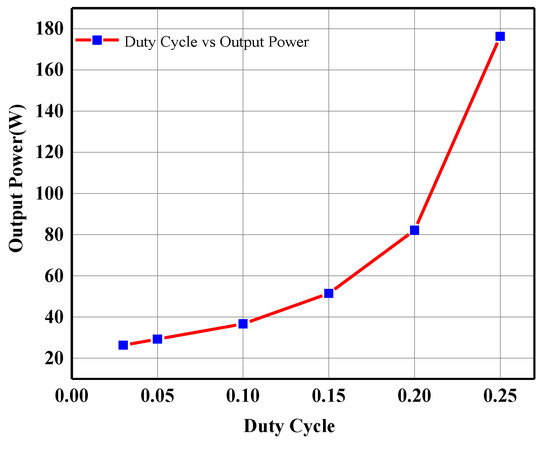
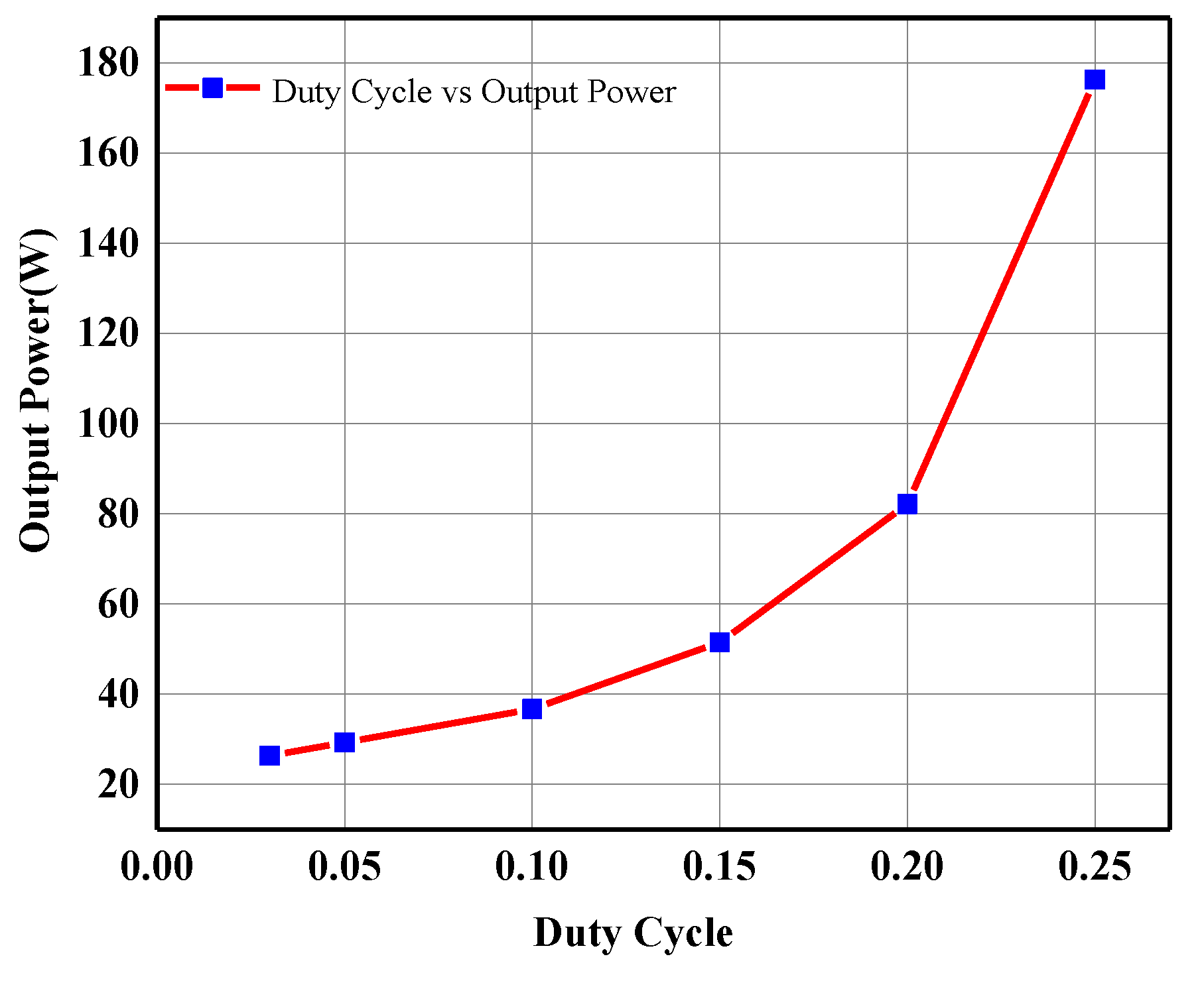
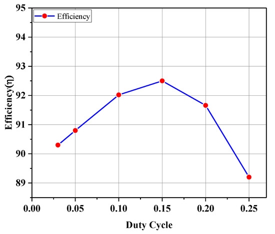
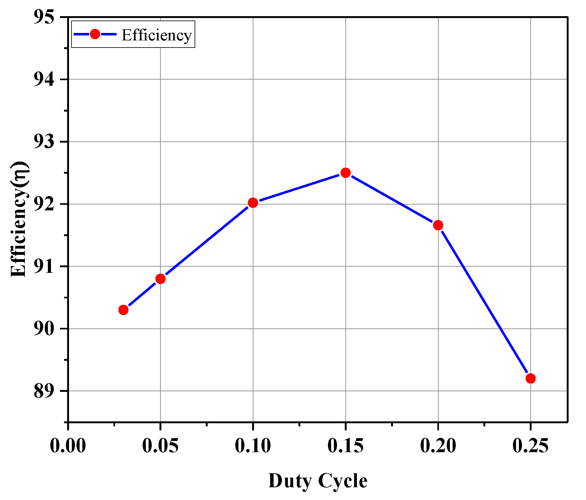
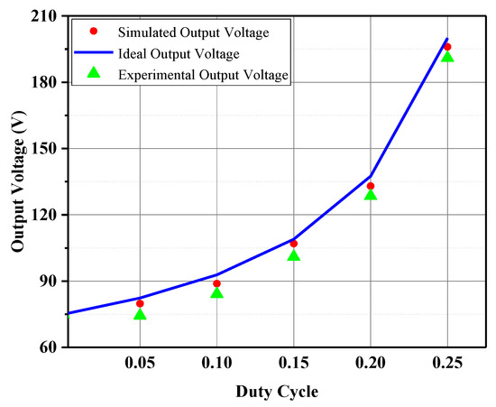
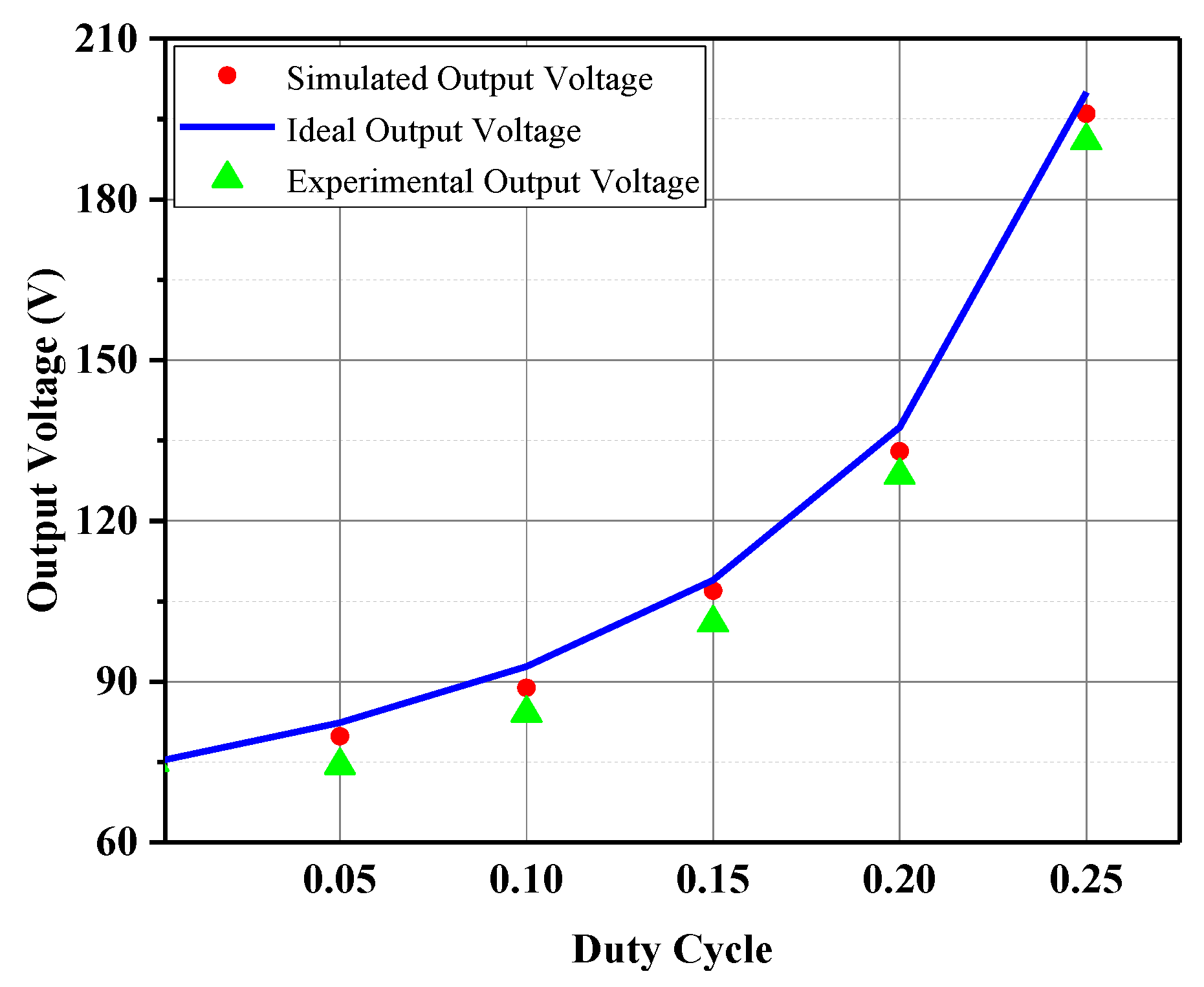
Figure 19 describes the distribution of losses among all the components, i.e., inductor, capacitor, switch, diode, etc. From Figure 19, it can be derived that the diode contains the highest losses, which is 67.53% of the total power loss. However, the losses due to inductors, capacitors, and switches are 13.82%, 2.66%, and 15.98%, respectively. The sensitivity of the output power with respect to the duty cycle is shown in Figure 20. It can be noticed that a small change in the duty cycle causes a large variation on the output voltage and thus on the output power. This can be further verified by considering the value of the duty cycle from 0.20 to 0.25 in Figure 20. The output power at D = 0.20 is approximately 80 W; however, at D = 0.25, the output power increased drastically to 175 W. Apart from this, Figure 21 presents the experimental efficiency of the proposed circuit at different duty cycles. It is observable that the maximum efficiency of the proposed HS-SZC at a specified duty cycle (D = 0.15) is greater than 92%. Figure 22 shows the sensitivity of the output voltage with variations in the duty cycle. Here, the output voltage is presented for ideal, simulated, and real conditions. The parasitic parameters are considered for the simulated output voltage. From Figure 22, it can be noticed that the ideal value of the output voltage for D = 0.15 is 109 V, while it is 107 V and 103 V for simulation and experimental conditions, respectively. This shows that ideal values calculated based on the theory comply with simulation and experimental results while showing a slight difference in the output voltage due to the presence of parasitic parameters. Hence, the optimization of these parasitic parameters will enhance the efficiency of the proposed design.
Figure 19.
Total power loss distribution at the duty cycle of 0.15.
Figure 20.
Variation of the output power at different duty cycles.
Figure 21.
Experimental efficiency vs. duty cycle graph.
Figure 22.
Ideal output voltage against the simulated output voltage with parasitic parameters and the experimental output voltage at different duty cycles.
10. Conclusions and Future Research
An advanced and efficient model of the switched Z-source DC-DC converter (HS-SZC) is presented in this study. The model is proposed using one inductor and switch at the backend of the conventional model of Z-source DC-DC converter and the derived voltage gain, i.e., (3 − 4D) / (1 − 3D) clearly specifies the significant improvement in the boost ability of the newly designed Z-source DC-DC converter. The theoretical voltage gain of 4.36 at D = 0.15 is achieved, while the simulation and experimental gains are recorded as 4.28 and 4.21, respectively. The proposed design obtains a higher gain at a very small duty cycle, i.e., D ≤ 0.33; thus, it eliminates the problems of the circuit complexity and larger duty cycle. Moreover, compared to the conventional Z-network converters, it utilizes a lower part count, which simultaneously reduces the cost and enhances the conversion efficiency. The proposed switched converter has a wide range of load capacity and voltage gains, which makes it suitable for applications with RESs. Finally, simulation and experimental results clearly justify the theoretical findings associated with the proposed converter. Future research will deal with the employment of the proposed topology with real applications, i.e., inverter, PV panel, etc.
Author Contributions
Conceptualization, R.K. (Rahul Kumar) and R.K. (Ramani Kannan); methodology, R.K. (Rahul Kumar) and A.M.; formal analysis, N.B.M.N. and A.M.; investigation, N.B.M.N. and R.K. (Rahul Kumar); writing—original draft preparation, R.K. (Rahul Kumar) and A.M.; writing—review & editing, A.M. and R.K. (Ramani Kannan). All authors have read and agreed to the published version of the manuscript.
Funding
This research was supported by [Yayasan UTP Fundamental Research] under the grant number [Y-UTP 015LC0-069]. And the APC was funded by [Yayasan UTP Fundamental Research].
Data Availability Statement
No new data were created or analyzed in this study. Data sharing is not applicable to this article.
Acknowledgments
The authors would wish to acknowledge Universiti Teknologi PETRONAS (UTP) for providing all necessary facilities to support this research.
Conflicts of Interest
The authors declare no conflict of interest.
References
- Gira, N.; Dahiya, A.K. Solar PV-BES in distribution system with novel technique for DC voltage regulation. Eng. Sci. Technol. Int. J. 2020, 23, 1058–1067. [Google Scholar] [CrossRef] [Scilit]
- Ahmed, T.A.; Mohamed, E.E.; Youssef, A.-R.; Ibrahim, A.; Saeed, M.S.; Ali, A.I. Three phase modular multilevel inverter-based multi-terminal asymmetrical DC inputs for renewable energy applications. Eng. Sci. Technol. Int. J. 2020, 23, 831–839. [Google Scholar] [CrossRef] [Scilit]
- Chen, Y.; Member, S.; Huang, A.Q.; Yu, X.; Member, S. A High Step-Up Three-Port DC—DC Converter for Stand-Alone PV/Battery Power Systems. IEEE Trans. Power Electron. 2013, 28, 5049–5062. [Google Scholar] [CrossRef] [Scilit]
- Gu, B.; Dominic, J.; Lai, J.-S.; Zhao, Z.; Liu, C. High Boost Ratio Hybrid Transformer DC—DC Converter for Photovoltaic Module Applications. IEEE Trans. Power Electron. 2012, 28, 2048–2058. [Google Scholar] [CrossRef] [Scilit]
- Zubieta, L.E.; Lehn, P.W. A High Efficiency Unidirectional DC/DC Converter for Integrating Distributed Resources into DC Microgrids. In Proceedings of the IEEE First International Conference on DC Microgrids (ICDCM), Atlanta, GA, USA, 7–10 June 2015; pp. 280–284. [Google Scholar]
- Syam, M.S.; Kailas, T.S. Grid connected PV system using Cuk converter. In Proceedings of the 2013 Annual International Conference on Emerging Research Areas and 2013 International Conference on Microelectronics, Communications and Renewable Energy, Kanjirapally, India, 4–6 June 2013. [Google Scholar] [CrossRef] [Scilit]
- Sener, E.; Ertasgin, G. A 3-ph Grid-Connected Photovoltaic Inverter Utilizing Super-Lift Luo Converter. In Proceedings of the 2018 2nd International Symposium on Multidisciplinary Studies and Innovative Technologies (ISMSIT), Ankara, Turkey, 19–21 October 2018; pp. 1–5. [Google Scholar] [CrossRef] [Scilit]
- Saravanan, S.; Babu, N.R. Analysis and implementation of high step-up DC-DC converter for PV based grid application. Appl. Energy 2017, 190, 64–72. [Google Scholar] [CrossRef] [Scilit]
- Padmanaban, S.; Kabalci, E.; Iqbal, A.; Abu-Rub, H.; Ojo, O. Control strategy and hardware implementation for DC-DC boost power circuit based on proportional–integral compensator for high voltage application. Eng. Sci. Technol. Int. J. 2015, 18, 163–170. [Google Scholar] [CrossRef] [Scilit]
- Shahir, F.M.; Babaei, E.; Farsadi, M. Voltage-Lift Technique Based Nonisolated Boost DC-DC Converter: Analysis and Design. IEEE Trans. Power Electron. 2017, 33, 5917–5926. [Google Scholar] [CrossRef] [Scilit]
- Hu, X.; Gong, C. A High Gain Input-Parallel Output-Series DC/DC Converter with Dual Coupled Inductors. IEEE Trans. Power Electron. 2015, 30, 1306–1317. [Google Scholar] [CrossRef] [Scilit]
- Salehi, S.; Zahedi, N.; Kheirollahi, R.; Babaei, E. Ultra High Step-up DC-DC Converter Based on Switched Inductor-Capacitor Cells. In Proceedings of the 2019 10th International Power Electronics, Drive Systems and Technologies Conference (PEDSTC), Shiraz, Iran, 12–14 February 2019; pp. 367–372. [Google Scholar] [CrossRef] [Scilit]
- Tang, Y.; Fu, D.; Wang, T.; Xu, Z. Hybrid Switched-Inductor Converters for High Step-Up Conversion. IEEE Trans. Ind. Electron. 2015, 62, 1480–1490. [Google Scholar] [CrossRef] [Scilit]
- Prudente, M.; Pfitscher, L.L.; Emmendoerfer, G.; Romaneli, E.F.; Gules, R. Voltage Multiplier Cells Applied to Non-Isolated DC-DC Converters. IEEE Trans. Power Electron. 2008, 23, 871–887. [Google Scholar] [CrossRef] [Scilit]
- Fang, X. A novel Z-source dc-dc converter. In Proceedings of the 2008 IEEE International Conference on Industrial Technology, Chengdu, China, 21–24 April 2008; pp. 8–11. [Google Scholar] [CrossRef] [Scilit]
- Galigekere, V.P.; Kazimierczuk, M.K. Analysis of PWM Z-Source DC-DC Converter in CCM for Steady State. IEEE Trans. Circuits Syst. I Regul. Pap. 2012, 59, 854–863. [Google Scholar] [CrossRef] [Scilit]
- Takiguchi, T.; Koizumi, H. Quasi-Z-source dc-dc converter with voltage-lift technique. In Proceedings of the IECON 2013 - 39th Annual Conference of the IEEE Industrial Electronics Society, Vienna, Austria, 10–13 November 2013; pp. 1191–1196. [Google Scholar] [CrossRef] [Scilit]
- Yang, L. A Quasi-Z -Source DC-DC Converter. In Proceedings of the 2014 IEEE Energy Conversion Congress and Exposition (ECCE), Pittsburgh, PA, USA, 14–18 September 2014. [Google Scholar] [CrossRef] [Scilit]
- Qiaojie, Z.; Yunxia, L.; Qiao, Y. Quasi-Z-source DC/DC converter based on switched inductor-capacitor unit and passivity based controller. In Proceedings of the 8th Renewable Power Generation Conference (RPG 2019), Shanghai, China, 24–25 October 2019; pp. 1–7. [Google Scholar] [CrossRef] [Scilit]
- Evran, F.; Aydemir, M.T. Z-source-based isolated high step-up converter. IET Power Electron. 2013, 6, 117–124. [Google Scholar] [CrossRef] [Scilit]
- Sharifi, S.; Monfared, M. Modified Series and Tapped Switched-Coupled-Inductors Quasi-Z-Source Networks. IEEE Trans. Ind. Electron. 2019, 66, 5970–5978. [Google Scholar] [CrossRef] [Scilit]
- Poorali, B.; Torkan, A.; Adib, E. High step-up Z-source DC-DC converter with coupled inductors and switched capacitor cell. IET Power Electron. 2015, 8, 1394–1402. [Google Scholar] [CrossRef] [Scilit]
- Zhang, G.; Zhang, B.; Li, Z.; Qiu, D.; Yang, L.; Halang, W.A. A 3-Z-Network Boost Converter. IEEE Trans. Ind. Electron. 2015, 62, 278–288. [Google Scholar] [CrossRef] [Scilit]
- Torkan, A.; Ehsani, M. A Novel Nonisolated Z-Source DC-DC Converter for Photovoltaic Applications. IEEE Trans. Ind. Appl. 2018, 54, 4574–4583. [Google Scholar] [CrossRef] [Scilit]
- Krishna, M.V.; Varma, L.T.V.; Kumar, M.A. Simulation of High Step up Z-Source DC-DC Converter with Voltage Multiplier Using Coupled Inductors. IJRAR Int. J. Res. Anal. Rev. 2018, 5, 594–598. [Google Scholar]
- Haji-Esmaeili, M.M.; Babaei, E.; Sabahi, M. High Step-Up Quasi-Z Source DC-DC Converter. IEEE Trans. Power Electron. 2018, 33, 10563–10571. [Google Scholar] [CrossRef] [Scilit]
- Zhang, G.; Iu, H.H.-C.; Zhang, B.; Li, Z.; Fernando, T.; Chen, S.-Z.; Zhang, Y. An Impedance Network Boost Converter with a High-Voltage Gain. IEEE Trans. Power Electron. 2017, 32, 6661–6665. [Google Scholar] [CrossRef] [Scilit]
- Shen, H.; Zhang, B.; Qiu, D. Hybrid Z-Source Boost DC-DC Converters. IEEE Trans. Ind. Electron. 2017, 64, 310–319. [Google Scholar] [CrossRef] [Scilit]
- Vaz, A.R.; Tofoli, F.L. Detailed design procedure of a DC-DC buck-boost converter employing a passive snubber. In Proceedings of the 2017 Brazilian Power Electronics Conference (COBEP), Juiz de Fora, Brazil, 19–22 November 2017; pp. 1–6. [Google Scholar] [CrossRef] [Scilit]
- H. P. International R. Mosfet. IRFP4768PbF. p. PD-97379. Available online: https://www.infineon.com/dgdl/irfp4768pbf.pdf?fileId=5546d462533600a40153562c959b2021 (accessed on 12 December 2016).
- Zeng, J.; Wu, J.; Liu, J.; Guo, H. A Quasi-Resonant Switched-Capacitor Multilevel Inverter with Self-Voltage Balancing for Single-Phase High-Frequency AC Microgrids. IEEE Trans. Ind. Inform. 2017, 13, 2669–2679. [Google Scholar] [CrossRef] [Scilit]
- Yang, L.; Qiu, D.; Zhang, B.; Zhang, G.; Xiao, W. A modified Z-source DC-DC converter. In Proceedings of the 2014 16th European Conference on Power Electronics and Applications, Lappeenranta, Finland, 26–28 August 2014. [Google Scholar] [CrossRef] [Scilit]
- Zhang, Y.; Liu, Q.; Gao, Y.; Li, J.; Sumner, M. Hybrid Switched-Capacitor/Switched-Quasi-Z-Source Bidirectional DC-DC Converter with a Wide Voltage Gain Range for Hybrid Energy Sources EVs. IEEE Trans. Ind. Electron. 2019, 66, 2680–2690. [Google Scholar] [CrossRef] [Scilit]
- Quasi-z-source, S.H.S.; Converter, D.C.D.C. Soft-Switched High Step-Up Quasi-Z-Source DC-DC Converter. IEEE Trans. Ind. Electron. 2020, 67, 4547–4555. [Google Scholar]
- Maalandish, M.; Hosseini, S.H.; Ghasemzadeh, S.; Babaei, E.; Jalilzadeh, T. A Novel Multiphase High Step-Up DC/DC Boost Converter with Lower Losses on Semiconductors. IEEE J. Emerg. Sel. Top. Power Electron. 2019, 7, 541–554. [Google Scholar] [CrossRef] [Scilit]
- Wu, G.; Ruan, X.; Ye, Z. Nonisolated High Step-Up DC—DC Converters. IEEE Trans. Ind. Electron. 2015, 62, 383–393. [Google Scholar] [CrossRef] [Scilit]
- Chen, M.; Li, K.; Hu, J.; Ioinovici, A. Generation of a Family of Very High DC Gain Power Electronics Circuits Based on Switched-Capacitor-Inductor Cells Starting from a Simple Graph. IEEE Trans. Circuits Syst. I Regul. Pap. 2016, 63, 2381–2392. [Google Scholar] [CrossRef] [Scilit]

Publisher’s Note: MDPI stays neutral with regard to jurisdictional claims in published maps and institutional affiliations. |
© 2021 by the authors. Licensee MDPI, Basel, Switzerland. This article is an open access article distributed under the terms and conditions of the Creative Commons Attribution (CC BY) license (https://creativecommons.org/licenses/by/4.0/).