Abstract
This paper presents a 10-bit 0.909-MHz 8-channel dual-mode successive approximation (SAR) analogue-to-digital converter (ADC) for brushless direct current (BLDC) motor drive, using a Taiwan Semiconductor Manufacturing (TSMC) 0.25 μm 1P3M Complementary Metal Oxide Semiconductor (CMOS) process. The sample-and-hold (S/H) circuit operates with two sampling modes. One is individually sampling eight channels in sequence with an S/H circuit and the other is sampling four channels simultaneously with four S/H circuits. All sampled data will be digitized with high-speed SAR ADC in time division multiplexing (TDM). A dynamic latch-type comparator is utilized to latch the output at an upper or lower level. The advantage of the designed comparator is that it performs with positive feedback to quickly complete the latch function. The double-tail latch-type architecture is utilized to mitigate the significant kickback effect by separating the pre-amplifier stage from the latch. By integrating an input NMOSFET with an input PMOSFET, the designed latch-type comparator can perform with full-swing input voltage. Measurements show that the signal-to-noise ratio (SNR), signal-to-noise-and-distortion ratio (SNDR), effective number of bits (ENOB), power consumption, and chip area are 50.56 dB, 57.03 dB, 8.11 bits, 833 μW, and 1.35 × 0.98 mm2, respectively. The main advantages of the proposed multichannel dual-mode SAR ADC are its low power consumption of 833 μW and high measured resolution of 8.11 bits.
1. Introduction
This paper proposed a 10-bit 2.27 MS/s successive approximation register (SAR) analog-to-digital converter (ADC) with two sampling modes and an eight-channel switch, which is usually used in the brushless direct current (BLDC) motor. BLDC motor is generally characterized by higher efficiency, lower maintenance, higher cost, and small volume [1]. A new digital control concept for BLDC machine has been introduced, experimentally verified, and implemented in a low-cost application-specific integrated circuit (ASIC). The field programmable gate array (FPGA)-based new digital pulse-width modulation (PWM) controller results in a considerable reduction of size and the cost of the system for BLDC motor drive [1]. Besides, the optical sensor can be used to measure the rotation speed of BLDC motor using the pulse width modulation (PWM) and the serial interface can be implemented using an energy-effective eight-bit SAR ADC [2]. To improve the performance of BLDC motor, integrating the ADC with control circuits is a good idea for electric vehicle, especially for high-voltage process. This idea had been published in [3] by integrating the permanent-magnet synchronous motor (PMSM) with a 10-bit SAR ADC.
To have low power consumption motor drive, the SAR ADC is popular for integration with electric vehicle control circuits because it performs with a continuous progressive characteristic and does not need a high-performance operational amplifier. A high-speed low-power SAR ADC circuit with 8-bit accuracy and 1.25 GSPS sampling rate had been published based on TSMC 28 nm CMOS technology [4]. Low power consumption and high accuracy are main advantages of SAR ADC [5]. Neither a micro-control unit (MCU), nor analog-to-digital converters (ADCs) are required with the proposed senseless architecture to achieve low-cost but high-performance sensorless control IC for BLDC motor, with wide speed ranges [6]. However, the whole architecture is evaluated with a FPGA-based system, which occupies great volume and operates with high power consumption.
Figure 1 shows the proposed control circuits of electric vehicle for BLDC motor, which is composed of digital controller, gate driver, detectors, SAR ADC, channel register, DC-DC buck converter, and BLDC Motor. The multi-channel detectors are used to detect and monitor those useful parameters, including average current, peak current, over current, temperature, speed, and so on. After those sensing data have been digitalized with SAR ADC, the digital control code can be fed into the controller and generates an appropriate pulse-width modulation (PWM) signal to control the gate driver and to drive the BLDC motor smoothly. In brief, the designed SAR ADC is a key component in BLDC motor drive. The rest of this paper is organized as follows. Section 2 elucidates the circuit design of the proposed SAR ADC and its relational circuits. Section 3 presents the post-layout simulation and measurement results, and the conclusion is drawn in Section 4.

Figure 1.
Proposed control circuits of electric vehicle for BLDC motor.
2. Circuit Design of the Proposed SAR ADC
Figure 2 shows the schematic of the proposed 10-bit SAR ADC with multiple inputs for BLDC motor drive. The proposed SAR ADC can be divided into five subcircuits, including the 8-way switch control system, sample and hold (S/H) circuit, digital-to-analog converter (DAC), comparator, and successive approximation register (SAR). The operational principle of the proposed SAR ADC is a binary search algorithm. It operates in three modes, including the sampling mode, hold mode, and charge redistribution mode.
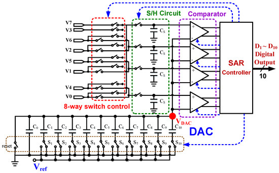
Figure 2.
Schematic of the proposed SAR ADC with multiple inputs for BLDC motor drive.
2.1. 8-Way Switch Control System
Figure 3 shows the designed 8-way switch control system, which is composed of three selection signals, se2–se0, to control 8 witches, t7–t0, and two mode signals, ma and mb. In the first sampling mode (M = 0), a set of S/H circuit (SH0) is assigned to sample 8 input signals (V7–V0) in sequence. The second sampling mode (M = 1) means that 4 sets of S/H circuits (SH3–SH0) are used to sample 4 input signals simultaneously. For an 8-way input signals, we need two steps to complete the second sampling mode. The first step (ma = 1) samples the most significant bit (MSB) group with 4 input signals, V7–V4. Next, the least significant bit (LSB) group (V3–V0) would be sampled in the second step (Mb = 1). Table 1 shows the control signals of the 8-way switch control system. In the first sampling mode (M = 0) (blue color), the input signal is determined with three selection signals, se2–se0 (yellow color), and is stored in the first S/H circuit (SH0) in sequence (red color)). In the second sampling mode (M = 1) (purple color), 4 input signals are sampled simultaneously. If the third selection signal se2 is set to 1, the MSB group, V7–V4, are sampled and stored in 4 S/H circuits, SH0–SH3, respectively (green color). On the contrary, the LSB group, V3–V0, are sampled and stored in 4 S/H circuits, SH0–SH3, respectively, when the third selection signal se2 is equal to 0 (pink color). The significant problem presented in the development of time-multiplexed channels is the inter-channel cross talk. Such cross talk may occur accidentally because of the long inductive leads, insufficient decoupling of circuits containing inductances, and other causes [7]. It is advisable to determine the effect on the phase response of slight variations in component tolerances. Phase-lock loop (PLL) is a good choice, not only to eliminate the phase variation, but also to mitigate the cross talk.

Figure 3.
Designed 8-way switch control system.

Table 1.
Control signals of the 8-way switch control system.
2.2. Proposed Sample and Hold Circuit
Figure 4 depicts the proposed sample and hold circuit, which is a switch with a constant gate to source voltage Vgs [8]. It is made of a sampling capacitor CS and a simple NMOSFET MA9 driven by the boosted driver to achieve both low power and wide bandwidth. The boosted driver produces a periodical output switching between VDD + Vin and the input voltage Vin. Two PMOSFETs, MA3 and MA5, are utilized to alleviate the errors induced by charge injection and clock feed-through because they conduct interactively. If clk = 0, then MA4 and MA8 turn on simultaneously. Next, the MA3 turns on because MA7 and MA8 are connected to ground. The sampling capacitor CS is charged to VDD rapidly. Besides, MA5 turns off by connecting to VDD through MA1 and two NMOSFETs, MA6 and MA9, are off by setting to ground through MA7 and MA8. Contrarily, if clk = 1, the MA5 turns on by setting the gate of MA5 to ground through MA2 and the source of MA5 to VDD, simultaneously. Note, both supply voltages, VDD and ground, are stored in the sampling capacitor CS in previous clock (clk = 0). After the MA5 turns on, the MA6 will be turned on. Therefore, the lower plate of Cs is connected to the input voltage Vin through MA6, and the upper plate of CS will be lifted up to VDD + Vin. Passing through MA5, the gate-source voltage Vgs of MA9 is fixed to VDD, regardless of the variation of input voltage Vin. That is, the output voltage Vout would not be adversely affected by the errors of MA6 and MA9, which are induced by charge injection and clock feed-through [2]. Note that all transistors, including NMOSFETS and PMOSFETs, are operating in saturation mode.
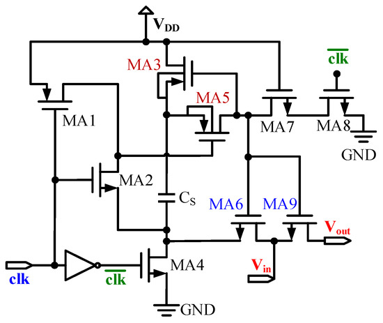
Figure 4.
Schematic of the proposed sample and hold circuit.
Table 2 shows the simulated results of the proposed S/H circuit with five design corners. The power supply, sampling frequency, input swing, and input frequency are 3.3 V, 5 MHz, 0-VDD, and 100 kHz, respectively. The effective number of bits (ENOB) and power consumption perform uniformly. The simulated differential nonlinearity (DNL) locates between −1 and +1 LSB. The performance of the proposed S/H circuit satisfies the required specification even though the simulated INL is larger than 1.0 LSB.
Table 2.
Simulated results of the proposed S/H circuit with five design corners.
2.3. Capacitive Digital-to-Analog Converter
In this study, a binary-weighted capacitive digital-to-analog converter (DAC) is considered to complete the required DAC circuit. The capacitive DAC performs with high density and high accuracy by combining the properties of the binary-weighted and the serial charge-redistribution DACs. This architecture operates with low integral nonlinearity (INL), good matching, and high tolerance to parasitic capacitance [9]. The designed DAC allows an efficient optimization based on the specifications of chip area, conversion speed, and linearity. Figure 5 shows the adopted 10-bit binary-weighted capacitive DAC with 11 capacitors denoted by C = {C0, C1, …, C10} with a ratio of C0: C1: C2: …: C10 be 1: 20: 21: 22: …: 29, respectively [10]. Then the total number of capacitors Ctotal are equal to 210 unit capacitors (C0).

Figure 5.
10-bit binary-weighted capacitive DAC.
For a 10-bit SAR ADC, we need 11 switches, S0–S10, and 11 conversion steps, Q0–Q10, to complete the conversion process. The first step (cycle) Q0 is a reset state, which is completed in the previous conversion process. In the reset state, the DAC voltage VDAC is connected to ground by setting S0 to 1 and the remainder switches, S1 − S10, to 0. In the second step (Q10), the switch S10 is set to 1 and the MSB capacitor is connected to the reference voltage VREF and the VDAC is charged into the half a reference voltage (=0.5 × VREF). If the input voltage VS/H, which is fed from the S/H circuit, is larger than VDAC, the output digital code is set to 1 (D10 = 1). Otherwise, the output code is 0. A register is used to store the output digital code and keep it until the end of the conversion process. Next, the switch S9 is set to 1 and the S10 is set to D10, a new VDAC is generated and compared to next input voltage VS/H. A new output digital code D9 is obtained and stored into the register. The following steps (Q8–Q1) will be completed in a similar fashion. Note that the last step is a reset state (Q0) (blue color in bold), which is prepared for the next conversion process. Table 3 presents the state table of the DAC switches and the output digital codes.
Table 3.
State table of DAC switches (S0–S10) and output digital codes (D).
2.4. Dynamic Comparator with Complementary Inputs
A comparator is an important circuit for designing SAR ADC. Both offset and complexities of the comparison process will seriously affect the accuracy and conversion rate of the designed SAR ADC. A dynamic latch-type comparator is utilized to latch the output at upper or lower level based on the voltage difference between two input nodes. The advantage of the designed comparator is that it performs with positive feedback to quickly complete the latch function. A voltage-type comparator has become especially popular because of their high input impedance, full-swing output, and absence of static power consumption [11].
The double-tail latch-type architecture, which was published in [11], is utilized to mitigate the significant kickback effect by separating the pre-amplifier stage from the latch [12]. To have a full-swing input, the designed comparator must limit the threshold voltage of PMOSFET and NMOSFET. For an input NMOS transistor, the latch-type comparator is limited to a lower limited voltage, which is equal to the threshold voltage of NMOS transistor (VthN). If an input PMOS transistor is only considered, an upper limited voltage, which is equal to VDD–VthP, is achieved with a threshold voltage of PMOSFET VthP. By integrating an input NMOSFET with an input PMOSFET, the designed latch-type comparator can compensate this shortcoming and perform with full-swing input voltage. Furthermore, the authors want to state clearly that the common-mode voltage Vcm of the comparator must be well controlled if the input is single-ended. As shown in Figure 6, if the inputs with large and small Vcm need to be processed by NMOSFET, and PMOSFET input transistors, respectively, the authors can expect they have differential offset and noise performances.
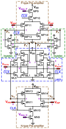
Figure 6.
Complementary-input double-tail latch-type voltage comparator.
Figure 6 presents the proposed complementary-input double-tail latch-type voltage comparator. If the clock signal CLK is set to 0, both NMOSFETs, ML5 and ML6, turn on simultaneously and the differential outputs, VOUTN and VOUTP, are connected to ground. The reset function is completed. In the meantime, MN10, MN13, and MN14 turn off, on, and on, respectively. Both outputs, NN and NP, are pulled up to VDD. Similarly, MP10, MP13, and MP14 turn off, on, and on, respectively, and both PN and PP are connected to ground. Next, MP15 and MP16 turn on and PN′ is connected to VDD, so does PP′. Then four PMOSFETs, ML7–ML10, turn off. Both outputs, VOUTN and VOUTP, are connected to ground stably and save the static power consumption. In the comparing mode, the clock signal (CLK) is set to VDD (1). Both MP10 and MN10 turn on and those outputs, PN, PP, NN, and NP, can be determined with two inputs, VINN and VINP. If VINP > VINN, then the voltage of NP is low (0) and ML10 conducts. Therefore, the positive output VOUTP is high (1) and ML1 conducts. The negative output VOUTN is low (0). Note that the discharge speeds of outputs, NN, NP, PN′ and PP′, are different due to the voltage difference between two inputs, VINN and VINP. Besides, if the input VINP is high (1) and the VINN is low (0), then the output VOUTP is high (1) and the VOUTN is low (0). This result verifies that the proposed comparator performs with positive feedback to achieve the latch function quickly. Two inverters are added between the P-type pre-amplifier and the latch stage to reverse the control signal and to guarantee that the output is high (1) through PMOS transistor and the output is low (0) via NMOS transistor.
2.5. SAR Controller
Figure 7 shows a logic circuit diagram of the conversion step, which is used to generate 11 step signals, Q0–Q10. Combining the step signals (Q0–Q10) with the output digital codes (D1–D10), the proposed DAC operates correctly by controlling those 11 DAC switches, S0–S10. Figure 8 presents the signal generation circuit of DAC switch Sn with integer n from 1 to 10. As shown in Figure 8, the Q0 and Qn are generated from Figure 7. The input signal of comp_end is an exclusive OR (XOR) function of VOUTP and VOUTN, which are shown in Figure 6. The reset signal RST is generated with clock signal (clk), logic circuit, and nonoverlap circuit. Figure 9 shows the simulated waveforms of DAC switches. The proposed circuit works correctly.
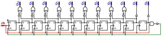
Figure 7.
Logic circuit diagram of the conversion step, which is used to generate 11 step signals, Q0–Q10.
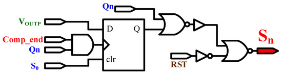
Figure 8.
Signal generation circuit of DAC switch Sn.
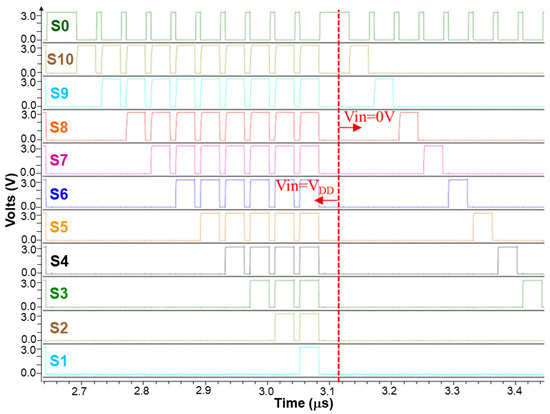
Figure 9.
Simulated waveforms of DAC switches.
3. Simulated and Measurement Results
Figure 10 shows the simulated power spectrum density (PSD) of the proposed sample and hold circuit. The 8192-point fast Fourier transform (FFT) simulation presents that the simulated SFDR is 71.51 dB, which is equal to 11.59 bits, at the input frequency of 100 kHz, sampling frequency of 5 MS/s, power supply of 3.3 V, and power consumption of 10.89 μW. As shown in Table 2, the simulated resolution of 11.59 bits at TT mode satisfies the design requirement of the sample and hold circuit in a 10-bit SAR ADC.
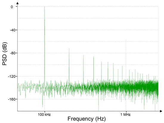
Figure 10.
Simulated power spectrum density (PSD) of the proposed sample and hold circuit.
As shown in Figure 6, if the common-mode voltage VCM is set to 0.1 V, two NMOSs, MN11 and MN12, turn off and two PMOSs, MP11 and MP12, turn on, simultaneously. Then four node voltages, NN, NP, PN, and PP, were pulled up to VDD and two node voltages, PN’ and PP’, were pushed down to ground by passing through inverters. As the differential input voltage ΔVin of 1.0 mV, the discharge rate are different at node voltages, NN, NP, PN’, and PP’. Then the differential output voltages, VOUTP and VOUTN, will be latched to VDD (3.3 V), and ground (0 V), respectively, by passing through the latch stage with cross-connected inverters and positive feedback. Figure 11 shows the simulation waveforms of the proposed comparator with VCM = 0.1 V and ΔVin = 1.0 mV.
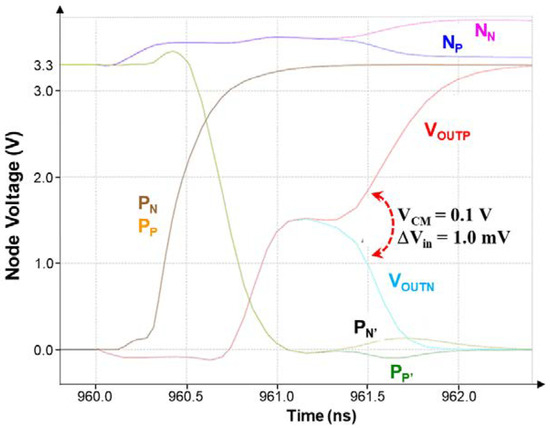
Figure 11.
Simulation waveforms of the proposed comparator with VCM = 0.1 V and ΔVin = 1.0 mV.
If the common-mode voltage VCM is set to 3.3 V, two NMOSs, MN11 and MN12, turn on and two PMOSs, MP11, and MP12, turn off, simultaneously. Then four node voltages, NP, NN, PP, and PN, were pushed down to ground and two node voltages, PN’ and PP’, were pulled up to VDD by passing through inverters. As the differential input voltage ΔVin of 1.0 mV, the discharge rate are different at nodes, NN, NP, PN’, and PP’. Thus the differential output voltages, VOUTP and VOUTN, were connected to VDD (3.3 V) and ground (0 V), respectively, by passing through the latch stage with cross-connected inverter and positive feedback. Figure 12 shows the simulation waveforms of the proposed comparator with VCM = 3.3 V and ΔVin = 1.0 mV. Note that the delay time is appropriately 1.86 ns at VCM = 0.1 V, whereas it is 1.24 ns at VCM = 3.3 V.
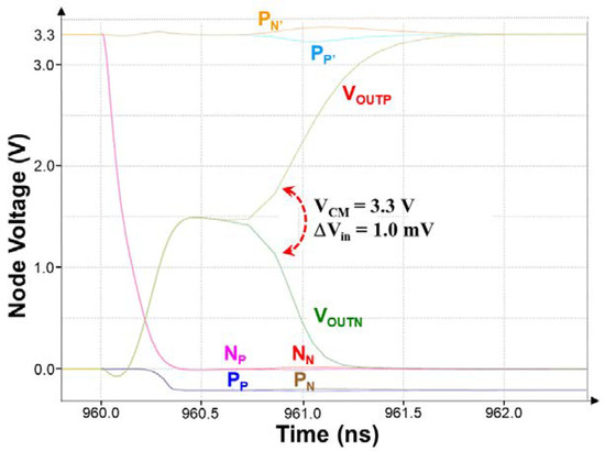
Figure 12.
Simulation waveforms of the proposed comparator with VCM = 3.3 V and ΔVin = 1.0 mV.
Figure 13 shows the post-layout-simulated PSD of the proposed SAR ADC. The simulated SNDR is about 65.88 dB and the ENOB is roughly 10.65 bits at input frequency of 110 kHz. The simulated resolution satisfies the specification of SAR ADC for use in BLDC motor drive. The simulation also presents that the DNL is +0.062/−0.501 dB, INL is +0.936/−0.081 dB, power consumption is 833 μW, and chip area is roughly 1.35 × 0.98 mm2 at TT corner. The proposed SAR ADC operates without missing code because the maximum DNL is less than 1 LSB. Table 4 summarizes the post-layout-simulated results of the proposed SAR ADC with three design corners. The SNDR and ENOB perform uniformly. The simulated performance of the proposed SAR ADC satisfies the required specification without missing code. Figure 14 shows the chip microphotograph of the proposed SAR ADC. A separation technique is considered to divide the large capacitor into two small capacitors and put them in common centroid. The small capacitor is put in the center of a circle, while the large capacitor is aligned outside the circle. Those parasitic impedance and capacitance can be reduced with symmetric layout. Furthermore, the temperature variation does not affect the resolution of the proposed SAR ADC from −40 °C to 100 °C. The simulated results satisfy the required specification of the proposed SAR ADC.
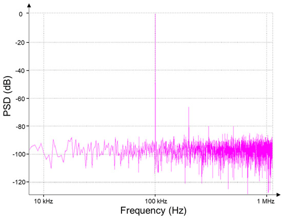
Figure 13.
Post-layout-simulated PSD of the proposed SAR ADC.
Table 4.
Post-layout-simulated results of the proposed SAR ADC with three design corners.
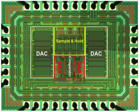
Figure 14.
Chip microphotograph of the proposed SAR ADC.
Figure 15 presents the measured printed circuit board (PCB) of the proposed SAR ADC with device under test (DUT). The signal generator (Anritsu MG3642A, Luton, UK) provided an input frequency of 110 kHz, the pulse data generator (Agilent 81130A, Ferrara, Italy) generated the clock frequency, the triple output power supply (Keysight E3631A) and precise DC power supply (Keysight N6761A, Santa Rosa, CA, USA) provided a power supply of 3.3 V and a bias voltage, respectively. The digital output code was captured by the logic analyzer (Keysight 16903A, Santa Rosa, CA, USA) and imported into the MATLAB environment for calculation of the SNDR and ENOB. Note that digital circuit (digital power) and analog circuit (analog power) were separated to prevent power interference in the DUT PCB.

Figure 15.
Measured DUT PCB of the proposed SAR ADC.
Figure 16 presents the measured 32,768-point PSD of the proposed SAR ADC with two sampling modes and an 8-channel switch at an input frequency of 110 kHz, a sampling frequency of 0.909 MS/s, and a power supply of 3.3 V. When a full-scale input sine wave was considered at the frequency of 110 kHz, the proposed SAR ADC yielded an SNDR of 50.56 dB, which was approximately 8.11 bits; this was achieved by setting two bias voltages, Vbias_N and Vbias_P, to 0.8 V, and 2.5 V, respectively. The measured resolution of 8.11 bits satisfies the specification of SAR ADC in BLDC motor drive because the PWM register contains an 8-bit channel. The DNL and INL are demonstrated in Figure 17 and Figure 18, respectively. The measured DNL varies from +0.99 LSB to −0.625 LSB and the measured INL changes from +1.28 LSB to −0.173 LSB. The proposed SAR ADC operates without missing code even though the measured INL is larger than 1.0 LSB. Note that the DNL/INL spurs are enlarged around code 50 and code 400 in Figure 17 and Figure 18, those negative impacts affect the measured results significantly.
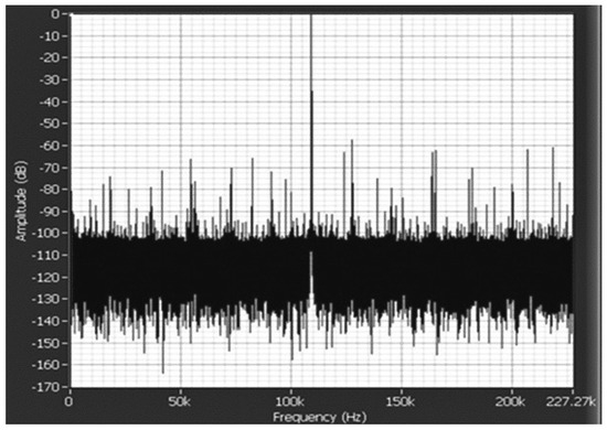
Figure 16.
Measured 32768-point PSD of the proposed SAR ADC at an input frequency of 110 kHz.
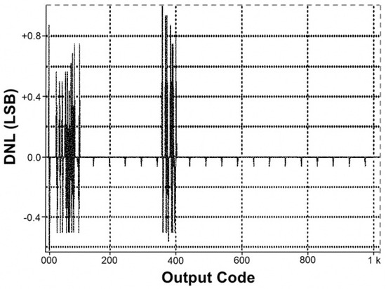
Figure 17.
Measured DNLs of the proposed SAR ADC.

Figure 18.
Measured INLs of the proposed SAR ADC.
Figure 19 shows the measured ENOBs with respect to input frequency at the sampling frequency of 0.909 MS/s. The measured ENOBs perform uniformly from 10 kHz to 110 kHz and the maximum SNDR occurs at 110 kHz. Note that the post-layout-simulated SNDR of 65.88 dB can be compared with the measured SNDR of 50.56 dB; the main difference was generated from the complementary-input double-tail latch-type voltage comparator. The sampled-and-held voltage VS/H was seriously affected by clock feedthrough phenomenon from N-type and P-type input stages. This impact caused the discrepancy between the measured and simulated SNDRs. Figure 20 shows the clock feed-through paths from N-type and P-type input stages at reset mode (CLK = 1 at N-type input stage). Besides, the second-order effects such as channel-length modulation and mismatch effects inside the S/H circuit need to be addressed in the future study [2].
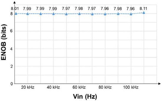
Figure 19.
Measured ENOBs with respect to the input frequency from 10 kHz to 110 kHz at the sampling frequency of 0.909 MS/s.
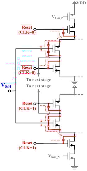
Figure 20.
Clock feedthrough paths from N-type and P-type input stages at reset mode (CLK = 1 at N-type input stage).
All the characteristics of the proposed 10-bit 0.909-MHz 8-channel dual-mode SAR ADC for BLDC motor drive are successfully verified. Table 5 summarizes the simulated and measured properties of the proposed SAR ADC developed herein and compares it with other SAR ADCs.
Table 5.
Performance summary and comparison with other SAR ADCs.
The performance comparison proved that the measured ENOB of this study is superior to those of References [12,16,17,23], and the power consumption of this chip is lower than those of SAR ADCs [13,14,15,17,19,22]. Furthermore, the simulated FoM of 0.57 pJ/conv.-step of this study is superior to those of 1.26 pJ/conv.-step in [15] and 175.5 pJ/conv.-step in [19], and the measured FoM of 3.316 pJ/conv.-step of this study is superior to those of 17.3 pJ/conv.-step in [18] and 30.9 pJ/conv.-step in [23]. Unfortunately, the measured FoM of this study is inferior to those of SAR ADCs [12,13,14,15,16,17,20,21,22]. The fabricated chip of this study suffers from clock feedthrough error, process variation, and thermal noise. Therefore, the post-layout simulation performs with a high post-layout ENOB of 10.65 bits, whereas a low ENOB of 8.11 bits was measured in our implemented chip. The FoM is defined as follows [17],
4. Conclusions
In this paper, we proposed a 10-bit 0.909-MHz 8-channel dual-mode SAR ADC for BLDC motor drive. The proposed sample and hold circuit is made of a sampling capacitor and a simple NMOSFET driven by the boosted driver to achieve both low power and wide bandwidth. A dynamic latch-type comparator is utilized to latch the output at upper or lower level. The advantage of the designed comparator is that it performs with positive feedback to quickly complete the latch function. The double-tail latch-type architecture is utilized to mitigate the significant kickback effect by separating the pre-amplifier stage from the latch. By integrating an input NMOSFET with an input PMOSFET, the designed latch-type comparator can perform with full-swing input voltage. By integrating the eight-way switch control system, sample and hold circuit, digital-to-analog converter, latch-type voltage comparator, and successive approximation register (SAR) into a whole chip of SAR ADC, the post-layout simulation proved that the SNR was 65.88 dB and the ENOB was 10.65 bits at an input frequency of 110 kHz and a sampling rate of 0.909 MHz. The main advantages of the proposed multichannel dual-mode SAR ADC are its low power consumption of 833 μW and high measured resolution of 8.11 bits. Unfortunately, the measured FoM of the proposed SAR ADC is inferior to those of other SAR ADCs, which are mostly fabricated in advanced process. Due to industrial requirements, this study was limited to design in TSMC 0.25 μm 1P3M CMOS process. Integrating SAR ADC with those control circuits, as shown in Figure 1, is a novelty and a contribution to the future projects, especially for the speed controller with microcontroller unit (MCU) [24,25].
Author Contributions
Conceptualization, G.-M.S., C.-H.H. and X.X.; methodology, C.-H.H. and S.-H.S.; formal analysis, C.-H.H., S.-H.S. and C.-H.H.; investigation, C.-C.H. and C.-H.H.; writing—review and editing, S.-H.S. and G.-M.S.; supervision, G.-M.S. and X.X.; project administration, G.-M.S.; funding acquisition, G.-M.S. and X.X. All authors have read and agreed to the published version of the manuscript.
Funding
This research was funded by the Ministry of Science and Technology (MOST), R.O.C., grant number MOST 109-2221-E-027-051 and by the NTUT-USTB Joint Research Program, grant number NTUT-USTB-109-02.
Acknowledgments
The authors would like to thank the Ministry of Science and Technology (MOST), Taiwan, for financially supporting this research. They are grateful to the Taiwan Semiconductor Research Institute (TSRI), Taiwan, for fabricating the test chip. This manuscript was edited by Wallace Editing.
Conflicts of Interest
The authors declare no conflict of interest.
References
- Sathyan, A.; Milivojevic, N.; Lee, Y.J.; Krishnamurthy, M.; Emadi, A. An FPGA-based novel digital PWM control scheme for BLDC motor drives. IEEE Trans. Ind. Electron. 2009, 56, 3040–3049. [Google Scholar] [CrossRef]
- Hong, H.C.; Lee, G.M. A 65-fJ/conversion-step 0.9-V 200-kS/s rail-to-rail 8-bit successive approximation ADC. IEEE J. Solid-State Circuits 2007, 42, 2161–2168. [Google Scholar] [CrossRef]
- Oh, J.; Heo, S.; Kim, M.; Suk, J.H.; Yang, Y.; Kim, J. High performance of PMSM driver IC integrated sensorless and current sensing circuits. In Proceedings of the 28th International Symposium on Power Semiconductor Devices and ICs (ISPSD), Prague, Czech Republic, 12–13 June 2016; pp. 251–254. [Google Scholar]
- Wang, Z.; Zhao, T.; Xu, D.; Chen, G.; Zhu, H.; Liang, F.; Zhang, G. Design of a low-power single-channel 8-Bit 1.25 GSPS SAR ADC. In Proceedings of the IEEE International Conference on Computation, Communication and Engineering (ICCCE), Longyan, Fujian, China, 8–10 November 2019; pp. 79–82. [Google Scholar]
- Mirzaie, N.; Alzahmi, A.; Lin, C.C.; Kim, I.; Byun, G.S. A low-power and performance-efficient SAR ADC design. In Proceedings of the International SoC Design Conference (ISOCC), Seoul, Korea, 5–8 November 2017; pp. 224–225. [Google Scholar]
- Cheng, K.Y. Novel architecture of a mixed-mode sensorless control IC for BLDC motors with wide speed ranges. In Proceedings of the Twenty-Fourth Annual IEEE Applied Power Electronics Conference and Exposition, Washington, DC, USA, 15–19 February 2009; pp. 2022–2027. [Google Scholar]
- Moskowitz, S.; Diven, L.; Feit, L. Cross-talk considerations in time-division multiplex systems. Proc. IRE 1950, 38, 1330–1336. [Google Scholar] [CrossRef]
- Liu, C.C.; Chang, S.J.; Huang, G.Y.; Lin, Y.Z. A 10-bit 50-MS/s SAR ADC with a monotonic capacitor switching procedure. IEEE J. Solid-State Circuits 2010, 45, 731–740. [Google Scholar] [CrossRef]
- Singh, R.R.; Genov, R.; Kotamraju, R.T.; Mazhari, B. Multi-step binary-weighted capacitive digital-to-analog converter architecture. In Proceedings of the 51st Midwest Symposium on Circuits and Systems, Knoxville, TN, USA, 10–13 August 2008; pp. 370–373. [Google Scholar]
- Li, Y.; Zhang, Z.; Chua, D.; Lian, Y. Placement for binary-weighted capacitive array in SAR ADC using multiple weighting methods. IEEE Trans. Comput. Aided Des. Integr. Circuits Syst. 2014, 33, 1277–1287. [Google Scholar]
- Schinkel, D.; Mensink, E.; Klumperink, E.; Tuijl, E.V.; Nauta, B. A double-tail latch-type voltage sense amplifier with 18ps setup+hold time. In Proceedings of the IEEE International Solid-State Circuits Conf. (ISSCC), San Francisco, CA, USA, 11–15 February 2007; pp. 314–315. [Google Scholar]
- Lai, W.C.; Huang, J.F.; Lin, W.J. 1 MS/s low power successive approximations register ADC for 67-fJ/conversion-step. In Proceedings of the IEEE Asia Pacific Conference on Circuits and Systems, Kaohsiung, Taiwan, 2–5 December 2012; pp. 260–263. [Google Scholar]
- Baek, S.Y.; Lee, J.K.; Ryu, S.T. An 88-dB Max-SFDR 12-bit SAR ADC with speed-enhanced ADEC and dual registers. IEEE Trans. Circuits Syst. II Exp. Briefs 2013, 60, 562–566. [Google Scholar] [CrossRef]
- Thirunakkarasu, S.; Bakkaloglu, B. Built-in self-calibration and digital-trim technique for 14-bit SAR ADCs achieving ±1 LSB INL. IEEE Trans. Very Large Scale Integr. VLSI Syst. 2015, 23, 916–925. [Google Scholar] [CrossRef]
- Jiang, Y.; Xi, J.; He, L.; Sun, K. A 16-channel 12-bit rail-to-rail successive approximation register ADC for AFEs. In Proceedings of the IEEE International Conference on Electron Devices and Solid-State Circuits (EDSSC), Hong Kong, China, 3–5 August 2016; pp. 263–266. [Google Scholar]
- Hong, H.C.; Lin, L.Y.; Chiu, Y. Design of a 0.20–0.25-V, sub-nW, rail-to-rail, 10-bit SAR ADC for self-sustainable IoT applications. IEEE Trans. Circuits Syst.-I Regul. Pap. 2019, 6, 1840–1852. [Google Scholar] [CrossRef]
- Li, D.; Liu, M.; Zhao, L.; Mao, H.; Ding, R.; Zhu, Z. An 8-bit 2.1-mW 350-MS/s SAR ADC with 1.5 b/cycle redundancy in 65-nm CMOS. IEEE Trans. Circuits Syst. II Exp. Briefs 2020, 67, 2307–2311. [Google Scholar] [CrossRef]
- Verma, D.; Shehzad, K.; Khan, D.; Kim, S.J.; Pu, Y.G.; Yoo, S.-S.; Hwang, K.C.; Yang, Y.; Lee, K.-Y. A Design of Low-Power 10-bit 1-MS/s Asynchronous SAR ADC for DSRC Application. Electronics 2020, 9, 1100. [Google Scholar] [CrossRef]
- Gao, B.; Li, X.; Sun, J.; Wu, J. Modeling of high-resolution data converter: Two-step pipelined-SAR ADC based on ISDMA. Electronics 2020, 9, 137. [Google Scholar] [CrossRef]
- Lin, C.-H.; Wen, K.-A. An Innovative Successive Approximation Register Analog-to-Digital Converter for a Nine-Axis Sensing System. J. Low Power Electron. Appl. 2021, 11, 3. [Google Scholar] [CrossRef]
- Liu, C.C.; Huang, M.C.; Tu, Y.H. A 12 bit 100 MS/s SAR-assisted digital-slope ADC. IEEE J. Solid-State Circuits 2016, 51, 2941–2950. [Google Scholar] [CrossRef]
- Roh, Y.J.; Chang, D.J.; Ryu, S.T. A 40-nm CMOS 12b 120-MS/s nonbinary SAR-assisted SAR ADC with double clock-rate coarse decision. IEEE Trans. Circuits Syst. II Exp. Briefs 2020, 67, 2833–2837. [Google Scholar] [CrossRef]
- Aiello, O.; Crovetti, P.; Alioto, M. Fully synthesizable low-area analogue-to-digital converters with minimal design effort based on the dyadic digital pulse modulation. IEEE Accesss 2020, 8, 70890–70899. [Google Scholar] [CrossRef]
- Xue, X.; Teh, Y.K. Power quality evaluation of six-step commutation brushless DC motor implemented on 32-bit ARM cortex microcontroller. In Proceedings of the 2020 IEEE Conference on Technologies for Sustainability (SusTech), Santa Ana, CA, USA, 23–25 April 2020; pp. 1–4. [Google Scholar]
- Taşören, A.E.; Orenbaş, H.; Şahin, S. Analyze and comparison of different PID tuning methods on a brushless DC motor using Atmega328 based microcontroller unit. In Proceedings of the 2018 6th International Conference on Control Engineering & Information Technology (CEIT), Istanbul, Turkey, 25–27 October 2018; pp. 1–4. [Google Scholar]
Publisher’s Note: MDPI stays neutral with regard to jurisdictional claims in published maps and institutional affiliations. |
© 2021 by the authors. Licensee MDPI, Basel, Switzerland. This article is an open access article distributed under the terms and conditions of the Creative Commons Attribution (CC BY) license (https://creativecommons.org/licenses/by/4.0/).