1. Introduction
In this paper, we present digital compensation of a resistive voltage divider (RVD), developed for digital sampling wattmeter application. This is a part of our current efforts in precise measurement of power in low frequency and radio frequency range [
1,
2]. The compensated RVD consists of a separate electrical circuit, and a digital compensation system based on National Instruments PXI-5922 digital acquisition cards (DAQ). While the frequencies in the power quality frequency range (e.g., below 3 kHz) are most important, frequencies needed or produced in electronic devices are constantly increasing, and many commercial power meters are declared by their manufacturers as being able to measure power up to MHz region [
3]. This has increased the demands on the calibration as well, and [
4] reports a watt meter standard for the audio frequency range (up to 100 kHz), while in [
3] a power measurement setup being able to measure power up to 1 MHz is described. In line with this, we present a method for digital compensation of RVDs with frequency range up to 100 kHz.
The input voltage of DAQs is generally in the range of several volts, where the peak input voltage of PXI-5922 is 10 Vpk-pk. Therefore, the input voltage to the wattmeter has to be lowered before digitizing, where inductive [
5] or resistive voltage dividers were applied. Since the design of inductive voltage dividers (IVD) with satisfying frequency bandwidth is very difficult, and due to the possible harmonic distortion generated by their ferromagnetic cores, the application of RVDs is recently enhanced. However, the RVDs are sensitive to the load impedance, which is consisted of the cable impedance and the input impedance of the digital acquisition card (DAQ) or a digital multimeter (DMM). To match the mainly capacitive load impedance, some sort of the impedance transformer, usually with operational amplifiers is often applied. As well, the additional capacitors, forming the auxiliary capacitive bridge can be applied, where the RVD is matched exclusively to a single cable length and type, and to a single input impedance of a specified DAQ or DMM [
6,
7,
8,
9].
The paper is organized as follows: in
Section 2, the design principles of the RVD are described,
Section 3 discusses the thermal effects of the RVD, while
Section 4 presents the measurement system for the system identification.
Section 5 describes the proposed Wiener compensation, and
Section 6 gives the results of its real-time implementation. Finally,
Section 7 is the conclusions.
2. Transfer Function of RVD
The electrical design of the RVD is described in detail in [
10]. The RVD is consisted of
n = 25 resistors with nominal values
R = 4.4 kΩ and a resistor with the nominal value
R0 = 2 kΩ (
Figure 1), thus giving the nominal voltage ratio
Here,
denotes input voltage and
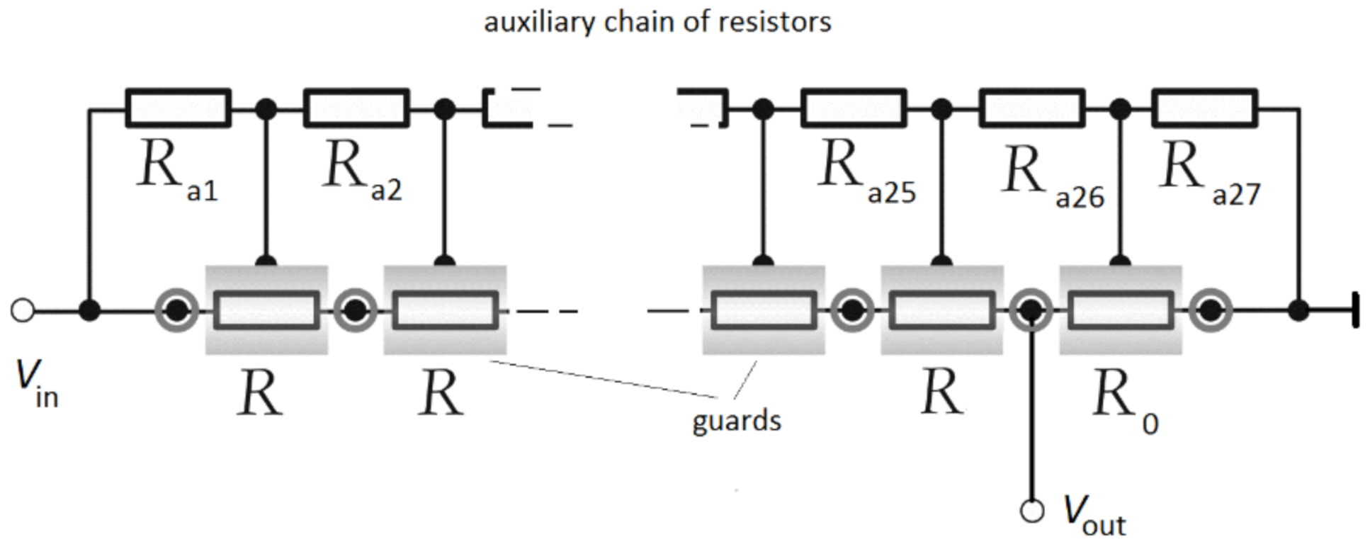
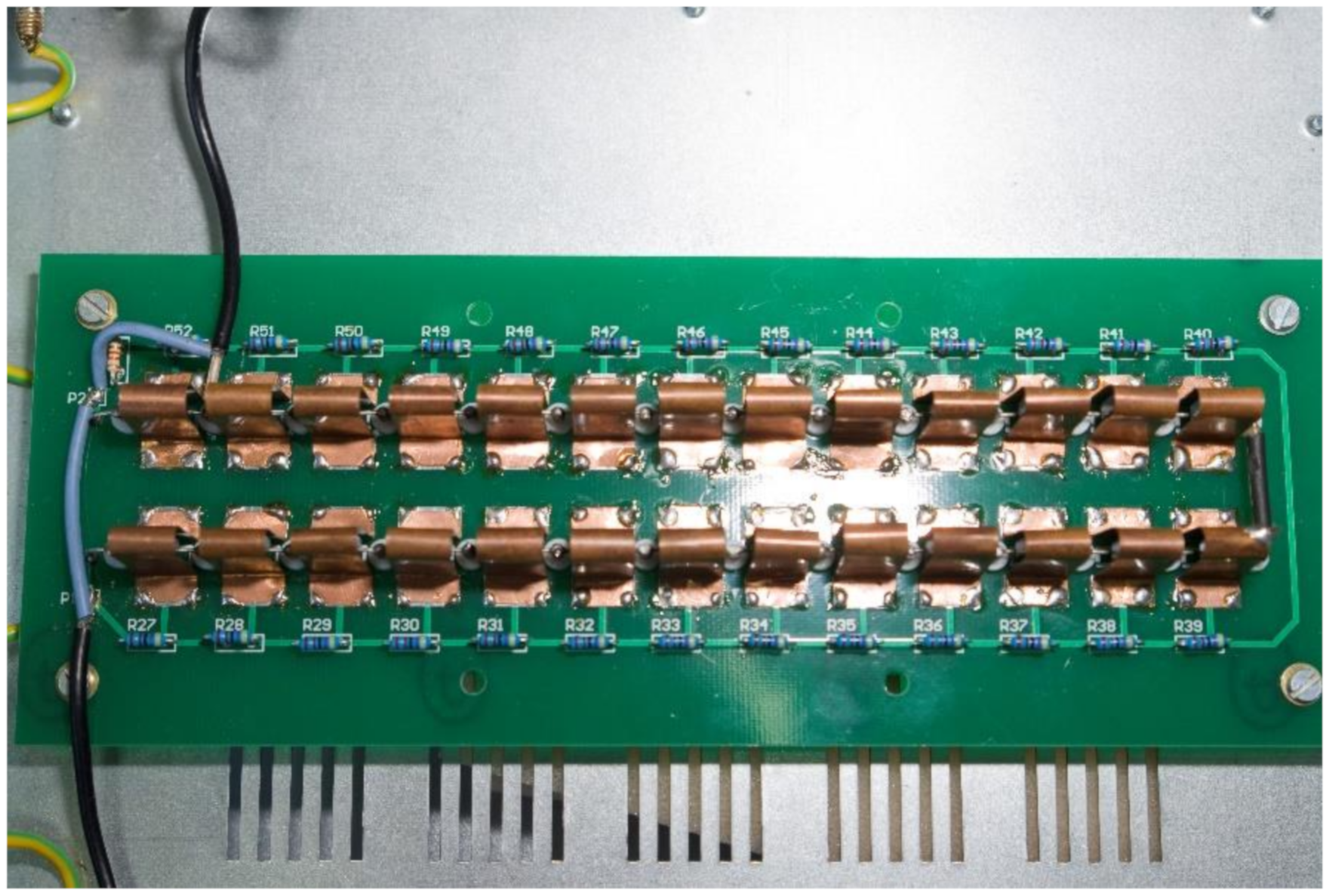
is output voltage of RVD. To minimize the influence of parasitic capacitances, the resistors are placed within individual copper guards. An auxiliary chain of resistors is applied to adjust the potentials of copper guards, thus minimizing the influence of parasitic capacitances (
Figure 2).
The resistors are Vishay S series bulk metal foil resistors, model number S102 C, soldered on the terminals with insulating rings. The mechanical and electrical basis for the RVD is a FR-4 custom-made printed circuit board. Note that only 26 resistors of the auxiliary chain are visible in
Figure 2, since the last resistor (Ra27) is mount-ed on the PCB perpendicularly to other resistors and therefore hidden by the cable. The considered frequency range (below 100 kHz) is low enough to allow the lumped parameter model to be applied in the analysis of the RVD circuit. Nevertheless, for the analysis of the circuit at very high frequencies the distributed parameter model with the transmission line parameters might be advantageous, but this can occur only at the GHz range, which is far beyond of the operation range of the RVD. Transfer function of the RVD is defined by an electrical network consisted of resistors and parasitic inductance and capacitance. In the phasor domain, it can be described as a complex ratio
Here,
denotes radian frequency. In [
11,
12] this transfer function was modeled by rational functions in the power quality frequency range (50 Hz–3 kHz). In such a black-box approach, a vector fitting tool was applied to build an off-line, s-domain model of the RVD. This modeling was aimed to provide the estimation (or interpolation) of the transfer function in the intermediate points between time-consuming precise measurements of the transfer function and optimization of the number of needed measurement points. In this paper, we propose a finite impulse response (FIR) digital inverse modeling of the RVD, aimed to ensure the digital compensation of this transfer function. This inverse modeling is implemented in real time using National Instruments PXI-5922 digital acquisition cards, thus lowering the errors of the divider.
3. Influence of Thermal Effect on RVD
The nominal input voltage of the divider is 560 V. The measurements of the transfer function can accurately be performed with a PXI system only at lower input voltage, due to the limitations imposed by the system. To verify the application of these measurements in the proposed method for the design of the compensation filter, the ratio of the divider was measured, applying nominal voltage and two different lower voltages. In this way, the possible change of the ratio due to the heating of the resistors can be evaluated. The measurements were performed applying DC voltages, thus having benefits of significantly lower measurement errors of digital multimeters (DMM) and the calibrator, and still achieving nearly the same heating effects as with corresponding AC voltages. For a purely resistive circuit, the dissipated power in the resistors will be the same for the applied AC and DC voltages if the Root Mean Square (RMS) value of the AC voltage is the same as the DC voltage. In the circuit from
Figure 1, the parasitic capacitances and inductances change the AC input impedance from the DC resistance, and consequently slightly change the current passing through the resistors. However, the DC measurements are giving the exact information of the change of the ratio of the resistance with different power dissipations. If this change is low enough for input voltages spanning from few volts up to the nominal 560 V, the results can be extrapolated to corresponding AC values as well. Note that the parasitic inductance of each resistor is very low: the maximum inductance of the resistors is 0,1 μH (0,08 μH typical), as declared by the manufacturer, and due mainly to the leads.
The ratio of the divider was measured for three different input DC voltages: 560 V, 197 V, and 3.53 V. First of them, i.e., 560 V was chosen as the nominal input voltage of the divider. The second voltage, i.e., 197 V is the maximum AC input voltage if the AC input voltage of the DAQ is at the maximum. Finally, 3.53 V is the maximum input voltage, allowed by DAQ, during the system identification. The purpose of these measurements was to identify the change of the ratio for different input voltages due to the thermal effects and to verify use of the identified transfer function for the measurement at higher and nominal input voltages. The measurement set-up consisted of a calibrator Transmille 3050A and two digital multimeters (DMM) HP3458A. Input and output of the RVD was measured with DMMs in Direct Current Voltage (DCV) mode. Both DMMs were synchronized and programmed in LabVIEW. A/D converter’s integration time is specified using NPLC (Number of power line cycles). NPLC is adjusted to ensure 8.5 digits of resolution (except for 100 mV DCV range which has a maximum of 7.5 digits). 100 samples were taken every 50 s and this process is repeated 60 times to get measurement period, i.e., observation period of 50 min. For each set of 100 samples, average value is calculated with related standard deviation. So, 50 mean values are obtained in 50 minutes. After the time period allowed for the stabilization of the ratio readings, the mean value of the RVD ratio at the nominal voltage (560 V)
was
= 55.9989761 with a standard deviation of 17.2 ppm (parts per million). This value is used as the reference in comparison with ratios measured with different input voltages. Note that this ratio differs from the theoretical nominal ratio
K = 560 V/10 V, due to the tolerances of the resistors. For input voltage equal to 197 V, the mean value of the ratio was 55.9973357 with a standard deviation of 11.6 ppm, and the ratio error in comparison to
was −29.29 ppm. Finally, for the input voltage equal to 3.53 V, the mean value of the ratio was 55.9979955 with a standard deviation of 56.9 ppm, and the ratio error in comparison to
was −17.50 ppm. For input voltage
= 3.53 V, the 1st DMM was in 100 mV DCV range and the 2nd DMM was in 10 V DCV range. For input voltages
= 197 V and
= 560 V, the 1st DMM was in 1000 V DCV range and the 2nd DMM was in 10 V DCV range.
Transmille 3050A has specified accuracy of 50 ppm +20 mV for the 220 V −1000 V range, 50 ppm + 0.3 mV for 200 V range and 50 ppm + 35 µV for 10 V range. Digital multimeter 3458A has less than 10 ppm of error on the whole DCV measurement range.
The change of the RVD ratio is for the decreased input voltage (applied at the system identification) small enough comparing to the ratio at the nominal input voltage. This qualifies the application of the measurements of the RVD frequency response, acquired with low input voltage, in the digital compensation for nominal and other considered input voltages. These small changes in the ratios (with applied voltage) are in line with very low temperature coefficient of resistance (TCR) of the applied resistors. It is °C with maximum spread °C, as declared by the manufacturer. Furthermore, the power dissipation of resistors is at the nominal input voltage below 20% (for it is below 10%) of their ambient power rating, as declared by the manufacturer. The small change of the ratios with different input voltages can be expected as well due to the balanced TCRs of resistors, the symmetrical structure of guards and leads, and small mass of the resistors. Therefore, it was not possible to observe and deduce the thermal time constant or any repeatable transient heating effect of the RVD ratio. There was only observed a short-term drift in measured ratio during the heating process, as well as during the measurements. Its value was estimated (using linear regression) to be approximately 1 ppm/hour, with possible source in the measurement set-up. The proposed Wiener compensation, being a frequency-dependent FIR model of a linear, time-invariant system does not include the change of its response with the value of the input voltage. Thus, it does not include the possible change of the RVD response with the change of the input voltage (retaining the same frequency) caused by the thermal effects. However, the above-presented measurements and accompanying analysis have shown that a FIR inverse model, designed on the basis of measurements taken with low input voltage is still applicable in the digital compensation with voltages spanning from few volts up to the nominal voltage.
4. Measurement System for System Identification
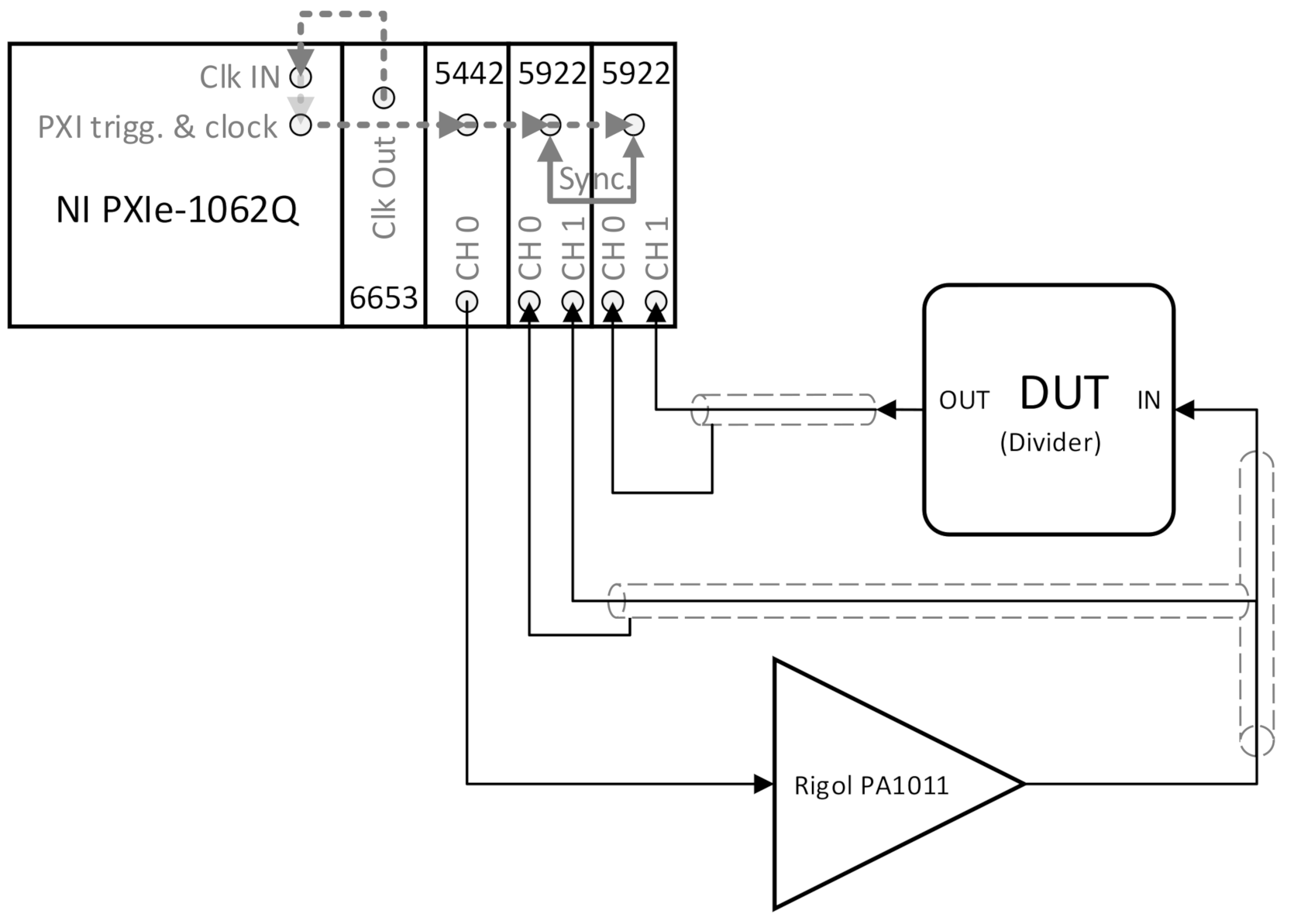
Measurement PXI setup is made of PXIe-1062Q chassis and PXI cards inserted in slots. In the first slot PXIe-8105 PXI embedded controller is placed, in the second slot PXI-6653 timing and synchronization control module, in the third slot PXIe-5442 PXI 16-bit 100 MS/s arbitrary waveform generator and in slots seven and eight two PXI-5922 Flexible resolution 24-bit PXI oscilloscopes are placed. The system timing slot (fourth slot in PXI-1062Q) is not used because the synchronization card used in this setup is not PXI express card. System timing slot is prepared for routing synchronization signals and clocks directly from synchronization card to PXI chassis clock signals without additional cables and external connections. A similar solution with both PXI synchronization card and PXI chassis can be made by placing PXI-6653 in the second slot of PXI chassis. Because of using PXI card and PXIe chassis, it was necessary to connect the signals with external cables and to program synchronization [
13]. The input impedance of PXI-5922 is 1 MΩ+/−2% paralleled with 60 pF typical, and its maximum input voltage is 10
. Its DC accuracy at 10
input range is +/− (500 ppm of input +100 μV).
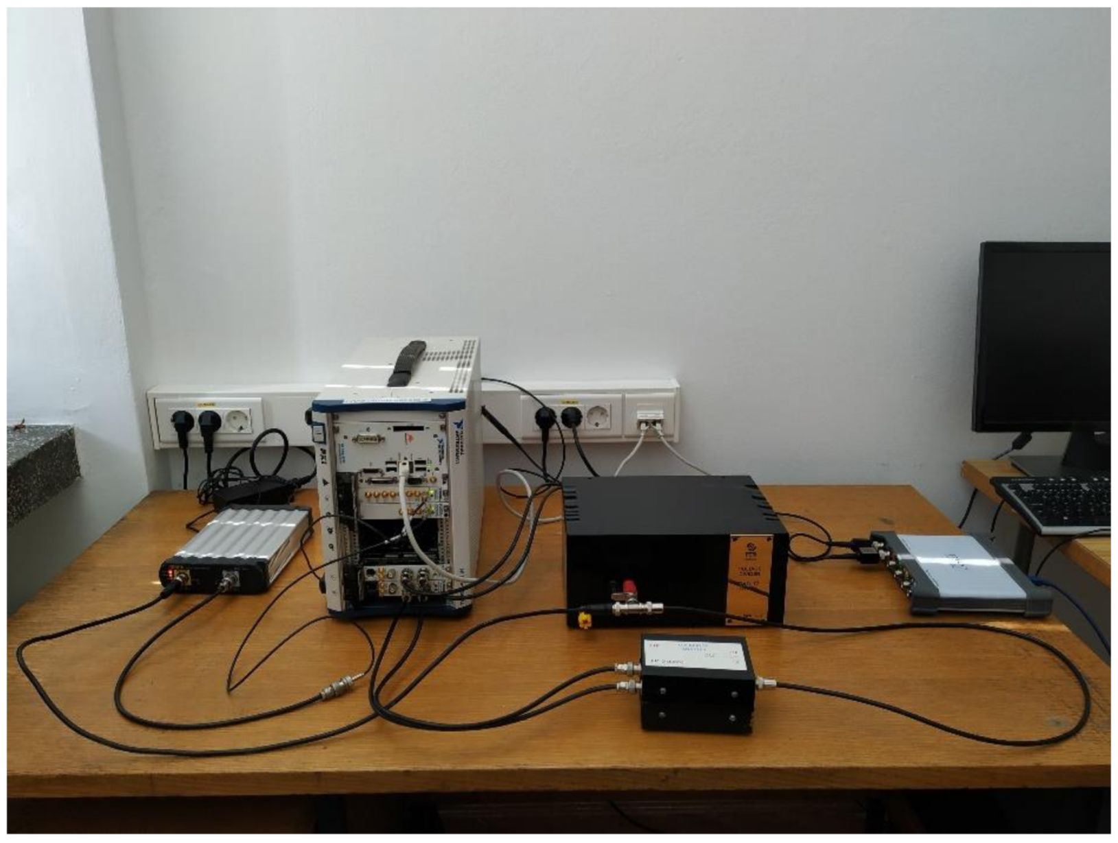
Figure 3 presents the block diagram of the measurement system, while
Figure 4 shows the measurement set-up.
The PXI-6653 synchronization card features a precision 10 MHz clock (OCXO) which accuracy is several orders of magnitude greater than the native 10 MHz clock of PXI backplane (PXI_CLK10). The OCXO is generated from oscillator circuit inside a sealed oven. With resistor heater and controlled feedback circuit temperature inside oven in PXI-6653 is precisely controlled. Temperature stability in 0 to 55 °C is 5 ppb (parts per billion), referenced to 25 °C. Long-term including stability of OCXO and supported circuitry is 50 ppb/year and initial accuracy is 3,2 ppb [
14].
The OCXO clock is in the beginning of code routed to out connector of PXI-6653. Software routing is made with National Instruments Synchronization (NI-SYNC) functions. The SumMiniature B (SMB) out connector is wired with 10 MHz Reference input Bayonet Neill–Concelman connector (REF IN BNC) on the back plane of PXIe-1062Q chassis. The OCXO replace the PXI Clock (PXI_CLK10) inside chassis which is then distributed through an independent buffer to PXIe-5442 PXI waveform generator and two PXI-5922 Flexible resolution PXI oscilloscopes. Skew between slots is less the 250 ps. Synchronization of two PXI-5922 card and homogeneous triggering is made with NI Trigger Clock (NI-TClk) Technology for Timing and Synchronization of Modular Instruments which used internal PXI chassis trigger bus [
15].
The coaxial cable for the connection of the RVD to the PXI-5922 card was the same that will be used in the sampling wattmeter application. In such a way, the load impedance, which affects transfer function of the divider, is the same as in the target wattmeter application. The load impedance consists of the cable capacitance shunted by the input impedance of the card. All inputs of the cards were configured in differential configuration.
The PXI system generates the stimulus signal, which is fed to the power amplifier PA1011. The signal from the power amplifier is brought to the input of the divider. The input and output voltages of the RVD are brought to a PXI-1062Q.
The needed software was entirely programmed in-house in the NI LabView environment. The measurement process starts with the definition of the frequency range, magnitude, and the set of replicate measurement for the averaging process. The communication between LabView application and the PXI system is accomplished using the Ethernet protocol and the institutional local area network (LAN), thus enabling distant start and control of the measurements. All parameters are transferred to the PXI client that adjusts the magnitude and frequency, performs the measurements, and sends the measurement results to the personal computer.
The measurement results consists of two main parts: the measurement of the magnitude response of the divider, and the measurement of the phase shift of the RVD. The magnitude response of the divider is in the sequel defined as
, where
denotes the input voltage and
denotes the output voltage. As well, the phase angle is defined as
where
denotes the phase angle of the output signal and
denotes the phase angle of the input signal.
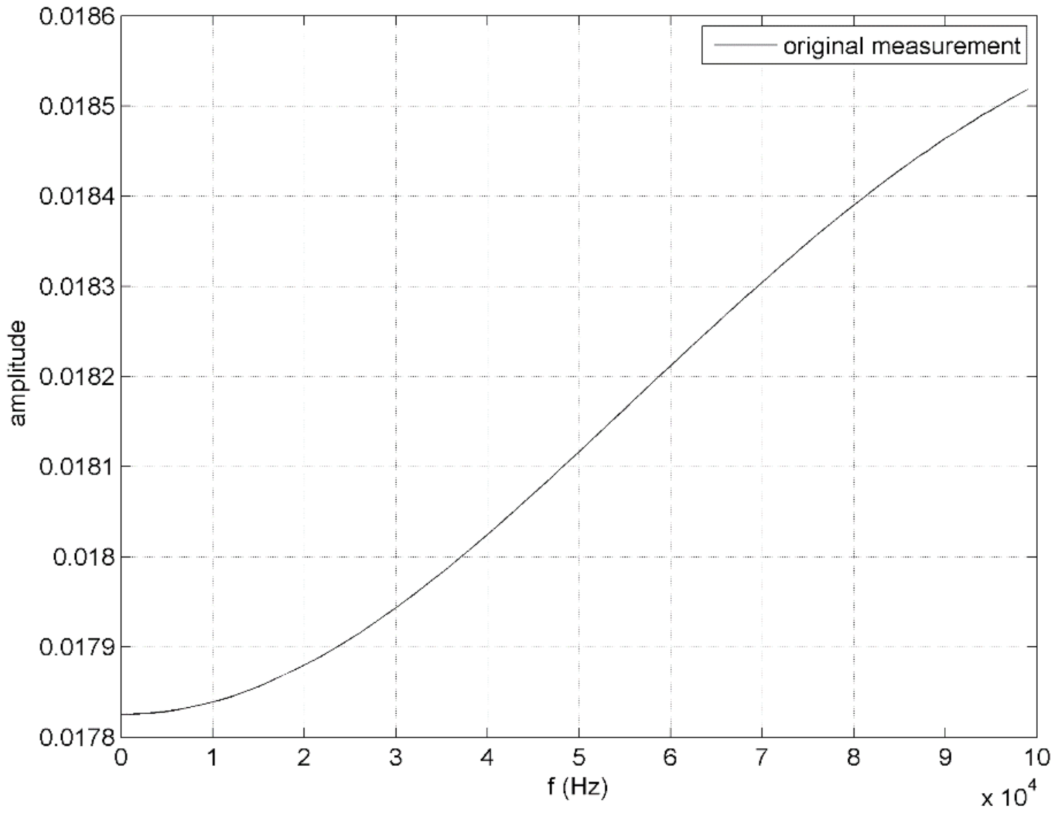
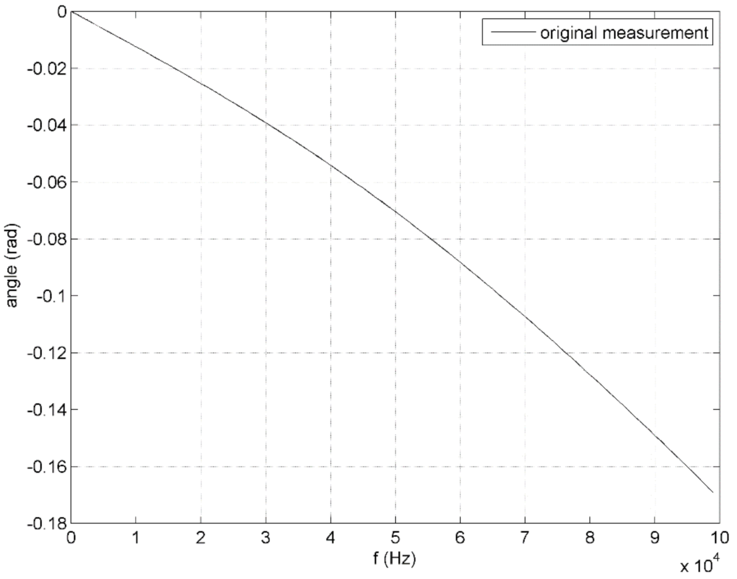
Figure 5 presents the magnitude response of the divider for the frequencies up to 100 kHz.
Figure 6 presents the phase response for the same frequency range. The measurements were taken at the non-uniform frequency-spacing of the samples. Up to 3 kHz the ratio and the phase shift was measured at the multiplies of 50 Hz and 60 Hz, starting from 50 Hz. For the frequency range between 3 kHz and 100 kHz the spacing between frequency samples was 1 kHz. Overall, 197 frequency samples were taken. The sampling frequency was changed adaptively: for frequencies below 1 kHz, it was 50 kS/s, for frequencies between 1 kHz and 10 kHz it was 500 kS/s, for frequencies between 10 kHz and 20 kHz it was 1MS/s, and for the frequency spanning from 20 kHz to 100 kHz it was 5 MS/s.
5. Wiener Compensation
The amplitude and the phase angle of the RVD can be compensated in real-time using a digital filter if the inverse transfer function is physically realizable. Unfortunately, it is not guaranteed that the transfer function of the RVD is the minimum phase. Hence, its inverse can be non-causal. In [
16] the problem of possible non-causality is solved by introducing a short time-delay in the identified inverse transfer function. Therefore, the delayed inverse will be causal since the negative time-portion of the impulse response of the non-causal inverse is shifted in time-axis toward the positive time. For a transfer function of the RVD measured in the frequency domain, the delay is introduced by the multiplication of the measured complex transfer function
H(
) with
. Here,
is the frequency in hertz,
T is sampling period and
is delay in samples. By introducing this delay, the transfer function of the delayed inverse in the z-domain is
. The desired time-delayed inverse frequency response can be expressed as a set of complex-valued elements.
where
defines magnitude response,
defines phase response, and
is the discrete set of frequencies. The frequency-domain synthesis of the finite-impulse-response (FIR) digital compensator can be achieved using an approach based on Wiener filtering, which was already applied in digital compensation of current instrument transformers [
16]. The set of filter coefficients
w of the compensator is defined by the time-discrete Wiener–Hopf equation [
17,
18].
Here,
R denotes the autocorrelation matrix
with the autocorrelations [
19]:
R is a symmetric Toeplitz matrix. Here, L is filter order and
is a positive weighting factor, which can be set individually for each frequency
. In such a way the specification of the transfer function can be held more tightly for some frequencies (with bigger weighting factors) than the others. In this particular application all
were set to 1 thus giving the equal emphasis on each specified frequency. Note that entries of the leading diagonal of
R reduce to:
p is the cross-correlation vector [
19]:
whose elements are cross-correlations
The system of equations defined by the Wiener–Hopf equation will have solution if matrix
R is a non-singular matrix (i.e., if it is invertible). In the frequency domain, it is satisfied with spectrally rich signals. Generally, the solution will exist if there are at least half as many frequency components in the measured response as there are coefficients in the Wiener filter [
18,
20].
6. Results
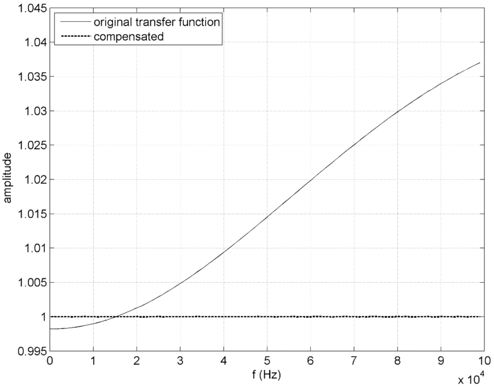
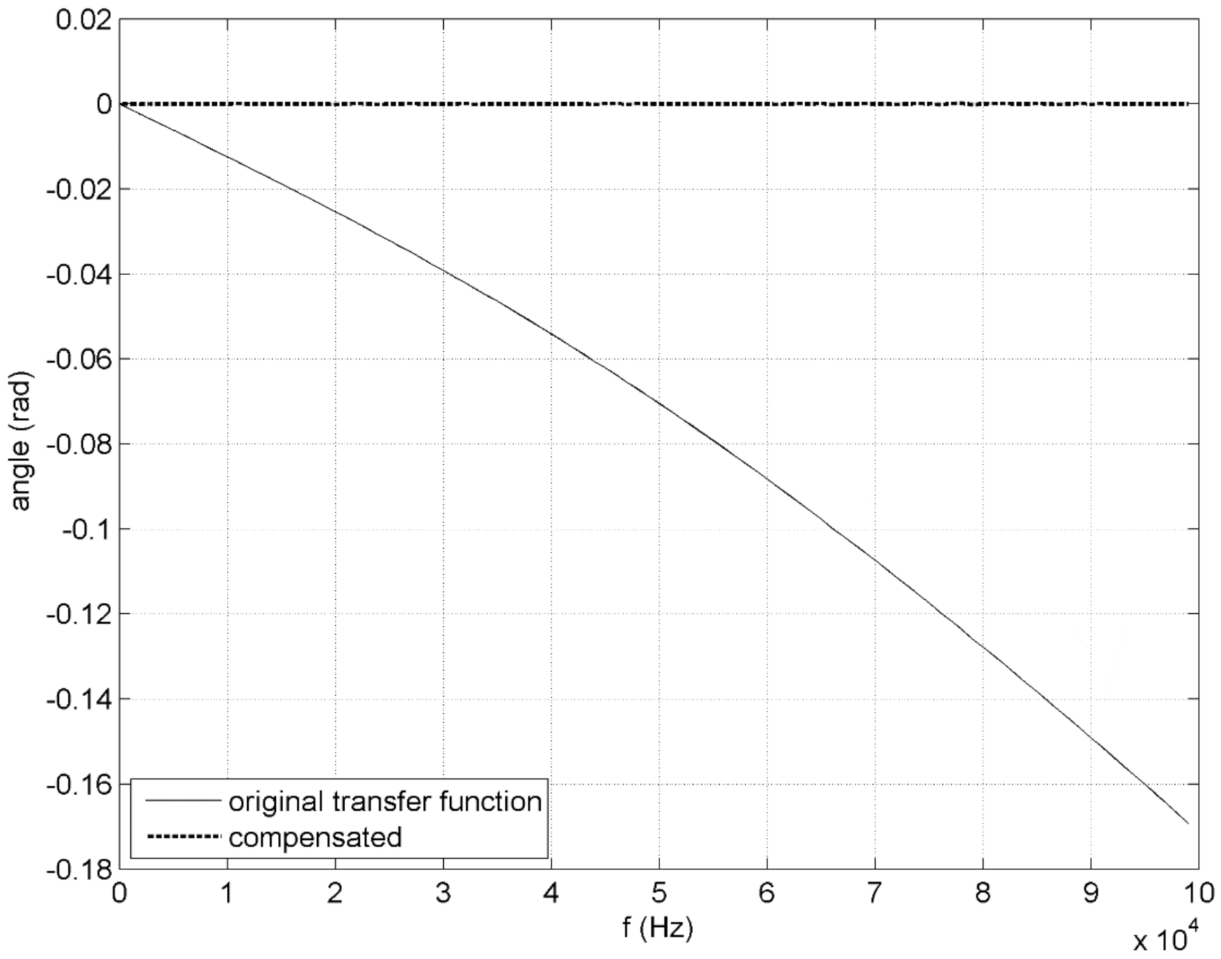
A routine in MATLAB was programmed for the Wiener compensation of the RVD. The filter order was 60, which gives satisfying results in the compensation and keeps additional time-delay low enough. The sampling frequency was 250 kHz, determined by the desired upper frequency limit in the compensation. Prior to the design of the FIR compensator, the measured transfer function was normalized by multiplication with the theoretical nominal ratio of the divider, e.g., with
. In such a way, the overall transfer function of the RVD and its digital compensator will have the magnitude response equal to the theoretical nominal ratio
K. Using the MATLAB routine, filters with added time delays from 0 to L/2 rounded were designed. On the basis of the minimum least-squares difference between measured and calculated responses, the optimum delay was determined. This optimal delay was 11 samples or 84 μs.
Figure 7 and
Figure 8 present the comparison of the normalized original transfer function and its digital compensation in MATLAB (magnitude and phase), after removal of time delay. The maximum errors of this fitting are below 40 ppm for relative magnitude error and 150 μrad for overall phase angle error.
Transfer function of the real-time implementation was measured using modified PXI-based system, applied in measurement for the system identification. The sampling function was set to 250 kHz, according to the filter design. Note that in system identification sampling frequency was changed adaptively for each frequency of interest. The same PXI system (
Figure 2) was also used for realization of Wiener compensation. All acquired data in measurement were processed through FIR function with coefficients defined by proposed procedure. Coefficients of FIR digital compensator are programmed into FIR.vi virtual instrumentation function from LabVIEW. The period of each measurement acquisition is long enough to preserve time for data processing and FIR compensation of RVD in real-time on PXI side.
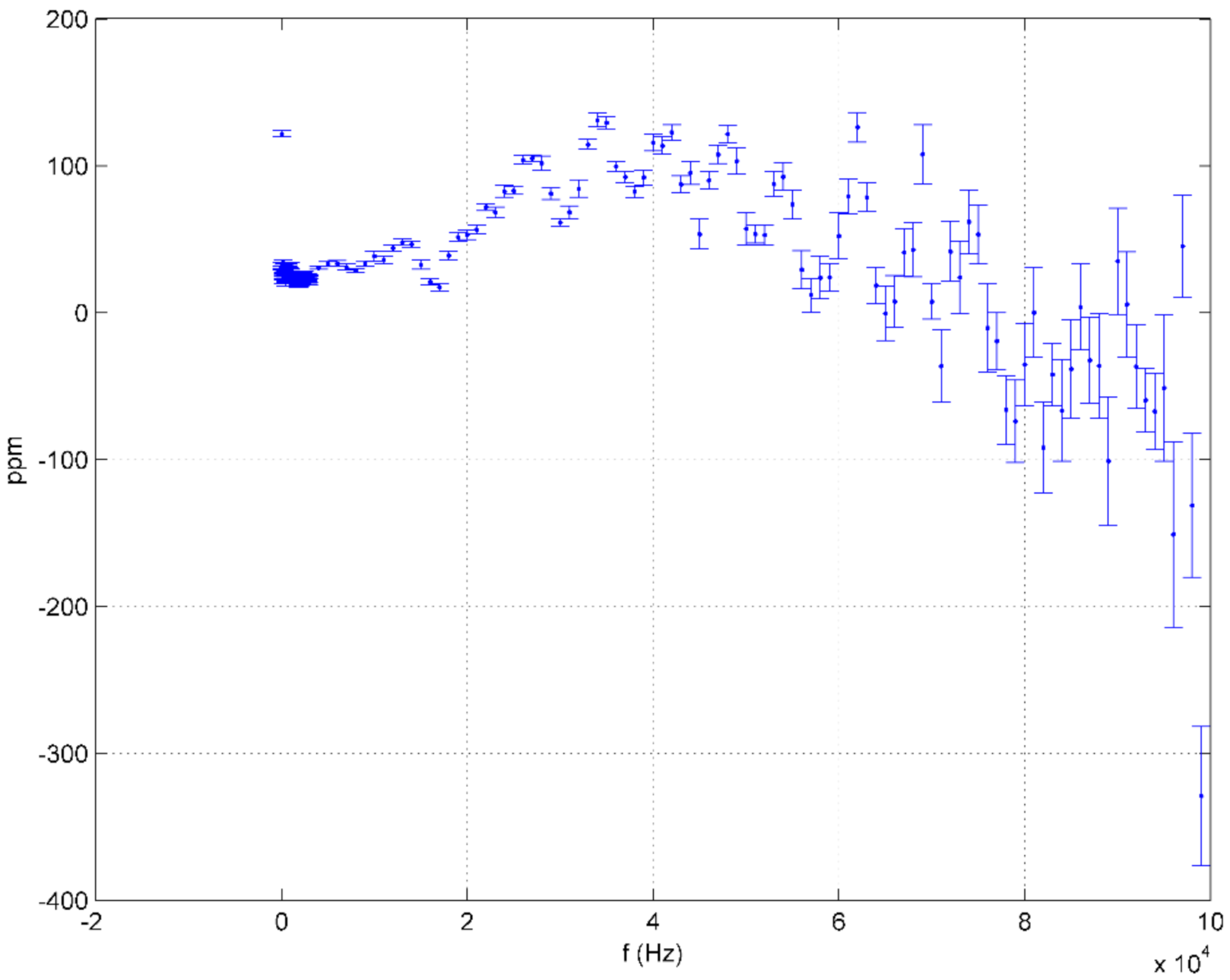
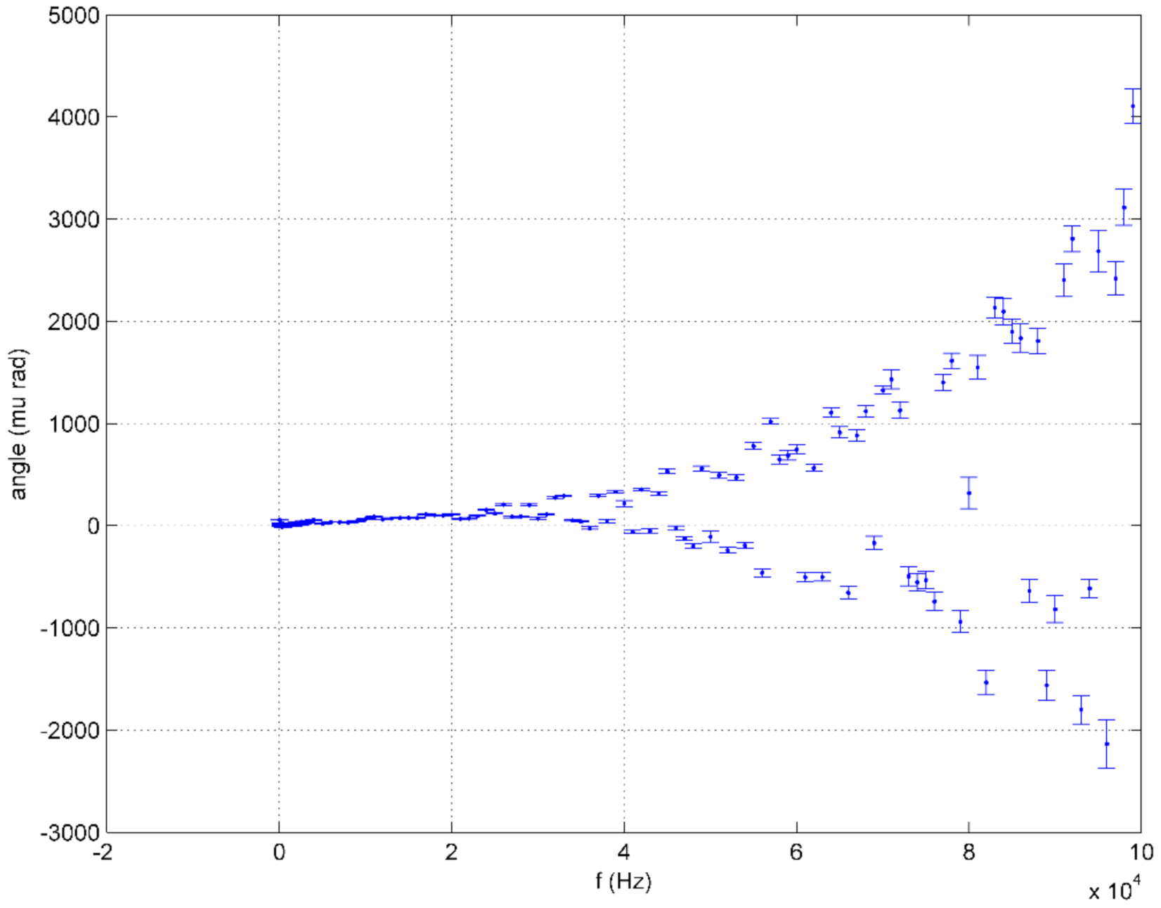
Figure 9 and
Figure 10 present magnitude error and phase angle error of the real-time compensated RVD after removal of time delay. The respective confidence intervals are indicated at each measurement frequency with error bars. At each examined frequency, the magnitude and phase angle were calculated based on
n = 100 independent successive measurements and associated standard deviation
s was calculated. Assuming normal distribution, the confidence intervals are calculated with coverage factor
k = 2, thus giving confidence level 95.44 % and confidence bounds
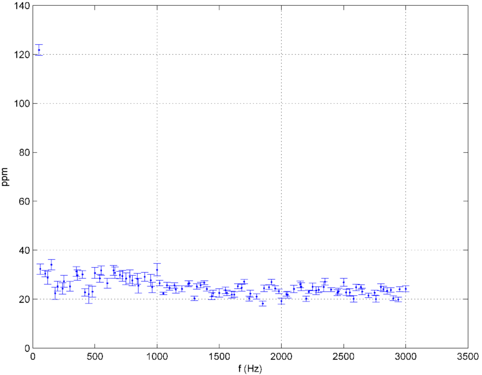
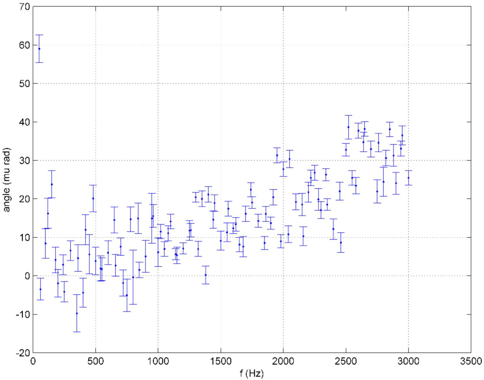
of the measured quantities. For the relative magnitude error in ppm, which is calculated (derived) from measured magnitude response, the associated confidence intervals were also recalculated from the confidence bounds of the magnitude response. To better visualize RVD errors in the power quality frequency range,
Figure 11 and
Figure 12 depict magnitude error and phase angle error in the frequency band spanning from 50 Hz to 3 kHz.
7. Conclusions
The digitally compensated resistive voltage divider intended for use in a sampling wattmeter application is developed. The proposed digital compensation, using FIR digital filtration and NI PXI DAQs, gives maximum magnitude error below 400 ppm and the phase angle error below 4500 μrad, in the frequency band 50 Hz–100 kHz. Those errors can mostly be attributed to the hardware and software limitations in the real-time implementation, while the proposed algorithm can mathematically fit the compensating transfer function with magnitude error below 40 ppm and overall phase angle error below 150 μrad, in the same frequency band. In the power quality frequency range (50 Hz–3 kHz) these errors were reduced below 130 ppm (maximum magnitude error) and 65 μrad (maximum phase angle error). The proposed approach with the digital compensation of RVDs allows the application of the same RVD with different DAQs and DMMs, and with different cable lengths, where digital compensation can be performed separately for different load impedances. As well, as the part of the re-calibration of the system, the re-calculation of the filter coefficients can be performed on the regular basis even for the same DAQ, thus allowing the fine-tuning of the compensation to adjust to the possible change in the original transfer function due to the aging of the components (RVD itself, cables, and DAQs). The proposed algorithm of the digital compensation allows use of non-uniform spacing of the frequency samples used for the determination of the FIR filter coefficients, which allows putting a greater emphasis on more important frequencies: the line frequency and its higher harmonics. The RVD will be used in wattmeter application in line with a set of precise current shunts of the cage type already developed at our laboratory.
Author Contributions
Conceptualization, M.D.; Methodology, M.D., P.M., and R.M., Software, M.D., P.M. and J.K.; Investigation, M.D., P.M., R.M. and J.K. All authors have read and agreed to the published version of the manuscript.
Funding
This paper is fully supported by Croatian Science Foundation under the projects Eddy current losses in open core of transformer under Grant IP-2020-02-2369 and Metrology infrastructure for support of the intelligent power grid under Grant IP-2019-04-7354.
Conflicts of Interest
The authors declare no conflict of interest.
References
- Konjevod, J.; Malaric, R.; Jurcevic, M.; Mostarac, P.; Dadic, M. Comparison of Digitizers for High-Precision Sampling Power Meters. IEEE Trans. Instrum. Meas. 2020, 69, 3719–3728. [Google Scholar] [CrossRef]
- Martinovic, Z.; Dadic, M.; Ivsic, B.; Malaric, R. An Adiabatic Coaxial Line for Microcalorimeter Power Measurements in Wireless Communication for Smart Grid. Energies 2019, 12, 4194. [Google Scholar] [CrossRef]
- Houtzager, E.; Rietveld, G.; Brom, H.E.V.D. Switching Sampling Power Meter for Frequencies Up to 1 MHz. IEEE Trans. Instrum. Meas. 2013, 62, 1423–1427. [Google Scholar] [CrossRef]
- Svensson, S. A watt meter standard for the audio frequency range. In Proceedings of the 1998 Conference on Precision Electromagnetic Measurements Digest (Cat. No.98CH36254), Washington, DC, USA, 6–10 July 1998; pp. 546–547. [Google Scholar]
- Kibble, B.P.; Rayner, G.H. Coaxial AC Bridges; Adam Hilger Ltd.: Bristol, UK, 1984. [Google Scholar]
- Hagen, T.; Budovsky, I. Development of a precision resistive voltage divider for frequencies up to 100 kHz. CPEM 2010 2010, 195–196. [Google Scholar] [CrossRef]
- Rydler, K.-E.; Svensson, S.; Tarasso, V. Voltage dividers with low phase angle errors for a wideband power measuring system. In Proceedings of the Conference Digest Conference on Precision Electromagnetic Measurements, Ottawa, ON, Canada, 16–21 June 2002; pp. 382–383. [Google Scholar]
- Mohns, E.; Ihlenfeld, W.G.K. A Precise Active Voltage Divider for Power Measurements. In Proceedings of the 2004 Conference on Precision Electromagnetic Measurements, London, UK, 27 June–2 July 2004; pp. 84–85. [Google Scholar]
- Wang, L.; Zhu, Z.; Huang, H.; Li, M.; Liu, L.; Lu, Z. Resistive voltage divider with two stage voltage buffer for harmonic measurement. In Proceedings of the 2012 Conference on Precision electromagnetic Measurements, Washington, DC, USA, 1–6 July 2012. [Google Scholar]
- Dadić, M.; Sandrić, B.; Mostarac, P.; Malarić, R. A Resistive Voltage Divider for Power Measurements. J. Energy-Energ. 2020, 69, 3–6. [Google Scholar] [CrossRef]
- De Souza, L.A.A.; Pinto, M.V.V.; Martins, M.B.; Lima, A.C.S. Modeling of a Resistive Voltage Divider by Rational Functions: Uncertainty Evaluation. IEEE Trans. Instrum. Meas. 2021, 70, 1–8. [Google Scholar] [CrossRef]
- Souza, L.A.; Pinto, M.V.V.; Martins, M.B.; De Lima, A. Modeling of a Resistive Voltage Divider by Rational Functions for Power Quality. In Proceedings of the 2020 Conference on Precision Electromagnetic Measurements (CPEM), Denver, CO, USA, 24–28 August 2020; pp. 1–2. [Google Scholar]
- Available online: http://www.ni.com/pdf/manuals/371843d.pdf (accessed on 1 September 2020).
- Available online: http://www.ni.com/pdf/manuals/370968a.pdf (accessed on 1 September 2020).
- Available online: http://www.ni.com/tutorial/3675/en/ (accessed on 1 September 2020).
- Dadic, M.; Mostarac, P.; Malaric, R. Wiener Filtering for Real-Time DSP Compensation of Current Transformers over a Wide Frequency Range. IEEE Trans. Instrum. Meas. 2017, 66, 3023–3031. [Google Scholar] [CrossRef]
- Stearns, S.D.; David, R.A. Signal Processing Algorithms; Prentice Hall: Englewood Cliffs, NJ, USA, 1988. [Google Scholar]
- Goodwin, G.C.; Sin, K.S. Adaptive Filtering: Prediction and Control; Prentice Hall: Englewood Cliffs, NJ, USA, 1984. [Google Scholar]
- Widrow, B.; Stearns, S.D. Adaptive Signal Processing; Prentice Hall: Upper Saddle River, NJ, USA, 1985. [Google Scholar]
- Nelson, P.A.; Elliot, S.J. Active Control of Sound; Academic Press: London, UK, 1992. [Google Scholar]
| Publisher’s Note: MDPI stays neutral with regard to jurisdictional claims in published maps and institutional affiliations. |
© 2021 by the authors. Licensee MDPI, Basel, Switzerland. This article is an open access article distributed under the terms and conditions of the Creative Commons Attribution (CC BY) license (http://creativecommons.org/licenses/by/4.0/).


