Article

The Characteristics of Aluminum-Gallium-Zinc-Oxide Ultraviolet Phototransistors by Co-Sputtering Method

1
Institute of Microelectronics & Department of Electrical Engineering, National Cheng Kung University, Tainan 70101, Taiwan
2
Institute of Microelectronics & Department of Electrical Engineering, Department of Photonics, National Cheng Kung University, Tainan 70101, Taiwan
*
Author to whom correspondence should be addressed.
Electronics 2021, 10(5), 631; https://doi.org/10.3390/electronics10050631
Submission received: 13 February 2021 / Revised: 3 March 2021 / Accepted: 4 March 2021 / Published: 9 March 2021
(This article belongs to the Special Issue Ultrasensitive Photodetectors and Applications)

Abstract

:
In this thesis, Aluminum-Gallium-Zinc oxide (AGZO) photo thin film transistors (PTFTs) fabricated by the co-sputtered method are investigated. The transmittance and absorption show that AGZO is highly transparent across the visible light region, and the bandgap of AGZO can be tuned by varying the co-sputtering power. The AGZO TFT demonstrates high performance with a threshold voltage (VT) of 0.96 V, on/off current ratio of 1.01 × 10⁷, and subthreshold swing (SS) of 0.33 V/dec. Besides, AGZO has potential for solar-blind applications because of its wide bandgap. The AGZO PTFT of this research can achieve a rejection ratio of 4.31 × 10⁴ with proper sputtering power and a rising and falling time of 35.5 s and 51.5 s.

1. Introduction

Oxide semiconductor materials have attracted considerable research in recent years due to their functions such as high transparency [1,2], flexibility [3,4], and low processing temperature [5]. Owing to the advantages above, oxide semiconductors have then been considered as high-performance thin film transistor (TFT) application candidates. Zinc oxide (ZnO), a II-VI compound semiconductor, has been widely reported for several advantages such as low toxicity, high conductivity, low cost because of its abundance on earth, large bandgap of 3.37 eV, and so on [6,7,8,9,10]. However, even though ZnO holds the edge as a candidate for device applications, innate defects such as oxygen vacancies and zinc interstitial, which may affect the performance of the device, cannot be ignored. Plenty of researchers have worked on this issue by incorporating appropriate metals into ZnO film. For example, Martins et al. demonstrated Indium-Zinc-Oxide (IZO) TFT with enhanced performances compared with ZnO TFT [11]. Other alloy oxide compounds such as ZTO [12], IGZO [3,13], ITZO [14,15], AZO [16,17], GZO [18,19] etc. have also been published.
Ultraviolet (UV) photodetectors (PD) also grab lots of interest these days because of their applications in ozone detectors, biological sensors, optical communication, remote controls, and military applications [20,21,22,23,24,25,26]. According to the wavelength, the UV can be divided into three regions: UV-A (λ from 320 nm to 400 nm), UV-B (λ from 280 nm to 320 nm), and UV-C (λ from 200 nm to 280 nm). Gallium oxide (Ga2O3), an ultrawide bandgap of larger than 4.4 eV oxide semiconductor, is then considered as a potential candidate of UV application, especially in the UV-C region. Although low carrier concentration and low mobility of Ga2O3 limit its application on devices, research on high power devices and ultraviolet photodetectors using the Ga2O3 compound as a channel layer can also be widely seen [3,13,27,28,29,30,31]. However, aluminum-gallium oxide (AGO) is still seldom mentioned in the academic literature.
In this study, we demonstrate thin film transistors with channel layers of aluminum-gallium-zinc-oxide (AGZO) with different ratios of ZnO and AGO. We adjust the composition of the channel layer by changing the radio frequency (RF) power of AGO. It is expected that with the ultrawide bandgap of AGO and carriers supplied by ZnO, a high-performance phototransistor can be obtained. The electrical and optoelectrical properties of the TFTs are also discussed.

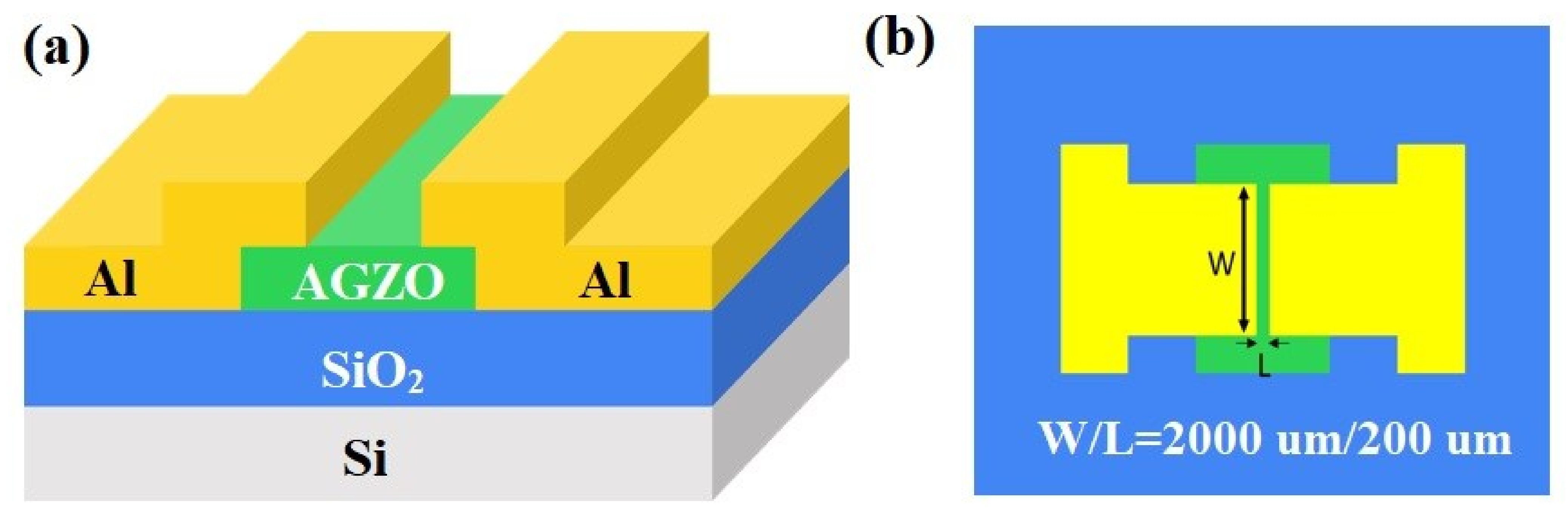
2. Materials and Methods

Before the fabrication of the device, the p-type silicon substrates (2 cm × 2 cm) with 200 nm SiO2 on top were cleaned with acetone, isopropyl alcohol, and deionized water for five minutes each in the ultrasonic oscillator. When it comes to the channel layer, we used the RF sputtering system to deposit the AGZO thin film. With the aids of RF sputtering system with an independent power source, we can easily vary the composition of the sputtered film by co-sputtering. During the sputtering process, the substrates were transferred into the co-sputtering chamber with background pressure and working pressure kept below 5 × 10⁻⁶ Torr and around 5 mTorr, respectively. The flow rate of Ar was fixed at 50 sccm and the substrates rotation speed of 15 rotations per minute to ensure the uniformity. One single target of ZnO and another single target of AGO (Al2O3:Ga2O3 = 5:95 in at%) were used. The sputtering power of the ZnO target was fixed at 60 W, while that of the AGO target varied from 20 W to 60 W with a step of 20 W. The total thickness of the channel was controlled at 20 nm. After deposition of the channel layer, we deposited 60 nm-thick Al electrodes on the samples by thermal evaporation. All the patterns are defined by shadow masks, and the schematic structure is illustrated in Figure 1.
TEM (JEM-2100F Electron Microscope, JEOL, Tokyo, Japan) was carried out to analyze the structure and composition of the device. The transmittance of the 100-nm-thick AGZO thin films deposited on quartz substrates (2 cm × 2 cm) was analyzed by UV-Vis-NIR spectrophotometer (U 4100, Hitachi, Tokyo, Japan). In order to analyze the content of oxygen vacancies, XPS (PHI 5000 VersaProbe, ULVAC, Japan) analysis was also conducted. The current-voltage (I–V) characteristics were obtained by Agilent B1500A semiconductor parameter analyzer (Agilent, Santa Clara, CA, USA). For the responsivity measurements, the monochromatic light, whose power was measured with a silicon photodiode, extracted from a 250-watt Xe arc lamp was used during the measurement of the photocurrent.

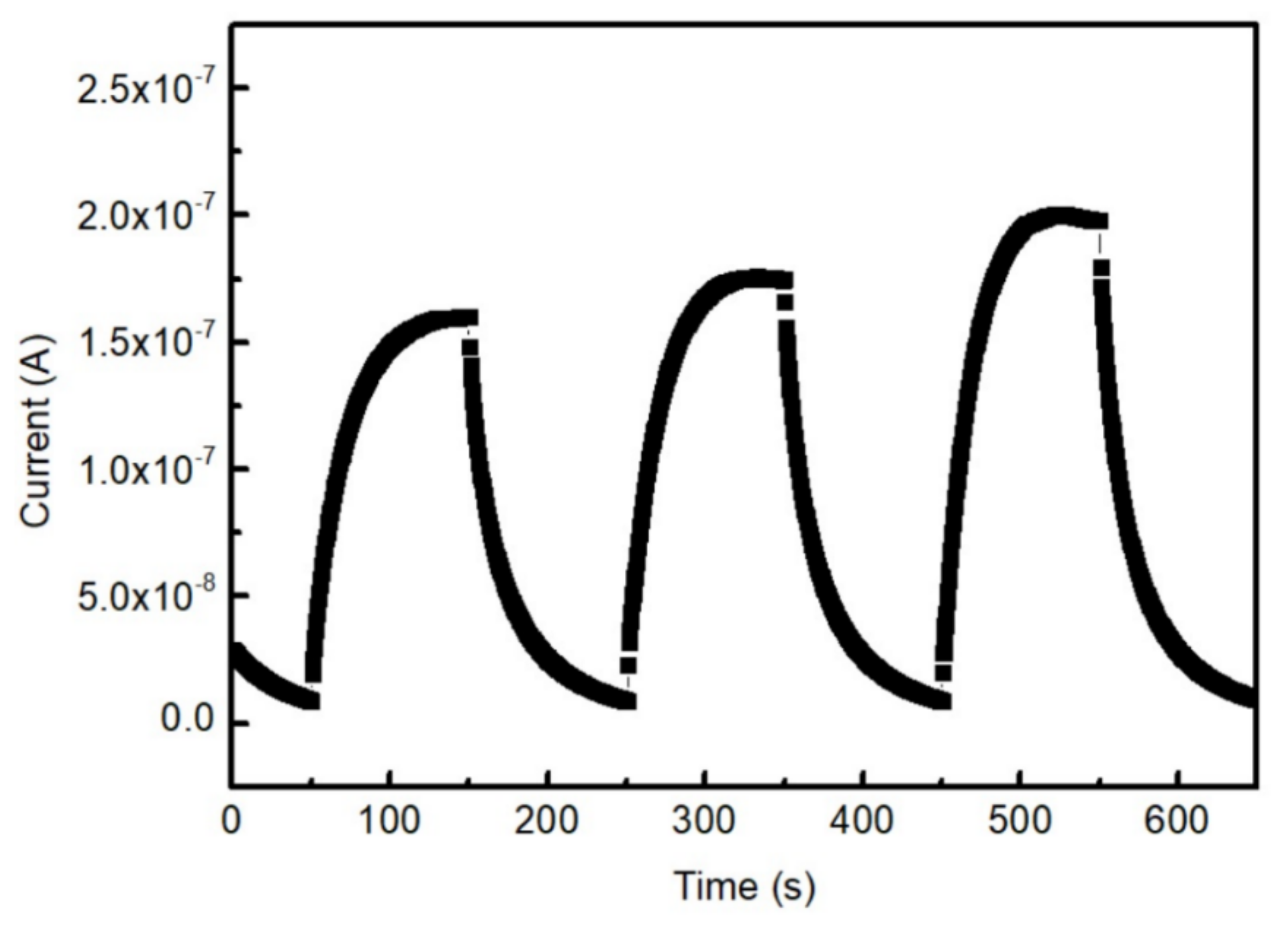
3. Results and Discussion

The TEM images of the AGZO PTFT sample with sputtering power ratio of 60:60 (W) (AGO:ZnO) are shown in Figure 2a. The device in the image is clearly separated into four layers, from bottom to top showing Si (bottom gate), SiO2 (gate dielectric), AGZO (channel layer), and Al (source and drain electrode). The thicknesses of the SiO2, channel layer, and Al electrode are 203.8 nm, 20 nm, and 60.56 nm, which are close to the estimated thicknesses. As a result, the thickness of each material while processing is well controlled. There is no significant lattice arrangement in the channel layer from HR-TEM image as shown in Figure 2b, which indicates that the as-deposited film is amorphous. With the aids of EDS analysis during TEM imaging, we can confirm the components of each layer as shown in Figure 2c.
To verify the bandgap of AGZO thin film with different sputtering power, the transmittance spectra of 100-nm-thick film under each power condition is shown in Figure 3. The three samples all depict high transparency over the visible region and start to absorb the light of wavelength shorter than about 400 nm, which indicates that AGZO is a promising material for UV photodetector applications. Besides, it is also observed that when the sputtering power of AGO grows from 20 W to 60 W, the transmittance curves result in a blueshift. From the Tauc equation, which describes the relationship of (αhν) and photon energy, can be written as (αhν)n = A(hν − Eg), where α is the absorption coefficient, h is the Planck’s constant, ν is the frequency of an incident light, A is a constant, and Eg is the bandgap energy [32]. Based on research conducted by Norlida et al. and Lee et al., who propose that ZnO and AGO are considered as direct bandgap material [33,34], we can infer that the compound AGZO which is co-sputtered by the two materials would stay the same. We use n = 2 due to the direct bandgap property of AGZO, and the Tauc plot could be obtained, as shown in the inset of Figure 3. The optical bandgap can then be estimated by obtaining the x-intercept (α = 0) of the tangent line to the inflection point of the (αhv)2 versus hv curve. As a result, the bandgaps of AGZO with different powers are 3.42 eV, 3.61 eV, and 4.03 eV when the power of AGO increases from 20 W to 60 W. Because the power of AGO increases, the bandgap is then dominated by AGO instead of ZnO, which leads to a larger bandgap. Table 1 summarized the composition of elements of the three samples according to the XPS analysis.
Figure 4a illustrates a typical n-type transfer characteristic from the AGZO TFT with different power ratio. The device was measured with drain voltage (VD) equal to 2 V and gate voltage (VG) sweep from −7 V to 15 V. Some important parameters are summarized in Table 2. The difference between the three samples can be explained by the content of oxygen vacancies in the channel layer. Figure 4b–d depicts the Gaussian fitting curves from the XPS result of the O1s peak of different AGZO thin films. The O1s peaks were deconvoluted into three peaks at 530.3 eV, 531.5 eV, and 532.2 eV, which are assigned to the well-bonded oxygen with metal cation (M–O), oxygen vacancies (Vo), and metal hydroxide species (M–OH), respectively. The content of oxygen vacancies can be obtained by calculating the area below the green curve divided by the total area of the sum. With power of AGO increasing from 20 W to 60 W, the content of oxygen vacancies can be extracted as 55%, 37%, and 26%, respectively; besides, the content of metal hydroxide species can be extracted as 18%, 21%, and 26%, which did not vary a lot. The higher power of AGO will result in more AGO in the film, which can suppress the oxygen vacancies. As a result, the film with power ratio of 60:60 has the least defect in the channel, the gate electrode thus has strong capability to take control of the channel, which leads to a better performance. The device with AGO: ZnO power ratio of 60:60 measured under illumination of wavelength from 240 nm to 500 nm is shown in Figure 5a. It is worth noting that the current at off-state increases when under illumination. Here, we can express the total drain current as ID’ = ID + Iphoto, where ID is the original current controlled by VG, and Iphoto is the photoconductive current generated by illumination [35]. When the TFT is operated in a dark environment, ID dominates ID’ at both off-state and on-state and results in a typical n-type transfer curve. However, when the TFT is under illumination, more and more photo-generated electron and hole pairs show up in the AGZO channel layer and increase the Iphoto. As a result, the drain current at off-state is then dominated by photo-induced current. Figure 5b illustrates the ID-VD output characteristics in dark and under illumination of 280 nm. It is obviously that the ID under illumination is much greater than in the dark.
To our knowledge, few groups have published semiconductor bandpass PTFTs or photodetectors. AlGaN is a candidate to fabricate bandpass optical devices, but it still needs to combine with other materials to reach this goal [36,37]. However, AGZO indicates a natural bandpass responsivity, which declines on both short and long wavelength sides, as shown in Figure 6. The responsivity is defined as the total current under illumination minus dark current and is divided by the light power. Figure 6a–c demonstrates the responsivity of devices with different power ratios. UV-to-visible rejection ratio (RR) is also an important parameter to identify a device. In this study, RR is defined as the responsivity measured at 270 nm divided by that measured at 440 nm. Besides, the best RR value appears at different VG of the three samples. According to Figure 6, the larger RR value usually appears at VG less than 0 V. When VG is positive, the total current would be mainly controlled by VG instead of the light, thus the responsivity under illumination and in the dark shows no significant difference and results in a smaller RR value. However, when VG is negative, the total current in the dark may also increase and lower the RR value [38,39,40]. Therefore, there is an optimized VG for each device to reach a higher RR value. The results are summarized in Table 3.
There is another interesting phenomenon that can be observed in Figure 6. Both responsivity in Figure 6a,b show a gradually decrease from a wavelength of 300 nm to 400 nm while it sharply cuts off in Figure 6c. This result can be explained by the responsivity of ZnO. Compared with AGZO TFT, the TFT with only ZnO as a channel layer is able to respond to a broad range of wavelengths, especially the light with wavelengths around 365 nm. The gradual decrease of the responsivity as mentioned might be attributed to more content of ZnO. Besides, owing to the high resistivity of Ga2O3 and its ability to suppress defects, when there is more Ga2O3 in the film, the responsivity of wavelength above approximately 320 nm will be smaller and will enhance the RR.
Since we recognized that the optimized power of AGO:ZnO is 60:60, the switching characteristics of the PTFT were analyzed. The current-time (I–T) characteristics of the devices were measured by switching the light source between off and on (wavelength of 280 nm) when operated at VG = −3 V and VD = 2 V, and the result is shown in Figure 7. The light source was kept for 100 s for each state and then switched to another for three cycles. The rise time refers to the time needed when the current increases from 10% to 90% of the peak value, and the fall time is the time needed when the current decreases from 90% to 10% of the peak value. The two parameters are crucial because they are indicators of how fast a photodetector can respond to the variation of the environment. The rise time and the fall time of the device was 35.5 s and 51.5 s, respectively. Furthermore, each cycle shows a similar current and reveals a similar off-current after turning off the light source. In summary, the result indicates that the AGZO PTFT has an excellent reliability and repeatability.

4. Conclusions

In this work, a TFT with AGZO as a channel layer was successfully fabricated by a co-sputtering AGO target and ZnO target. The influence of different power for each target on the performance was discussed. The TFT with AGO:ZnO equal to 60:60 depicted the best performance with Vt of 0.96 V, mobility of 0.04 cm2/Vs, on/off current ratio of 1.01 × 10⁷, and SS of 0.33 V/dec, respectively. Besides, the UV applications were also carried out. The AGZO TFT demonstrates a natural bandpass responsivity with highest responsivity of 0.014 A/W when under illumination of 270 nm and shows a high RR of 4.31 × 10⁴. I–T characteristics demonstrate that the device has quiet excellent reliability and repeatability with rise time and falling time of 35.5 s and 51.5 s. In summary, the fabricated TFT indicates that AGZO is a potential candidate for both the TFT switching device and UV sensing device. Through proper bandgap engineering, both innate of Ga2O3 and ZnO can be compensated by each other and can result in a potential material for future application.

Author Contributions

W.-L.H., C.-H.L. and S.-P.C. designed and performed the experiments, conceptualization and methodology, and analyzed the data. W.-L.H. and C.-H.L. wrote the manuscript in consultation with S.-J.C. and S.-P.C. All authors have read and agreed to the published version of the manuscript.

Funding

This research received no external funding.

Acknowledgments

This work was supported by the Ministry of Science and Technology under contract number MOST 107-2221-E-006-146; and the Advanced Optoelectronic Technology Center, National Cheng Kung University, for projects from the Ministry of Education. The authors gratefully acknowledge the use of JEOL JEM-2100F CS STEM equipment belonging to the Instrument Center of National Cheng Kung University.

Conflicts of Interest

The authors declare no conflict of interest.

References

  1. Nomura, K.; Ohta, H.; Ueda, K.; Kamiya, T.; Hirano, M.; Hosono, H. Thin-film transistor fabricated in single-crystalline transparent oxide semiconductor. Science 2003, 300, 1269–1272. [Google Scholar] [CrossRef]
  2. Fortunato, E.M.; Barquinha, P.M.; Pimentel, A.; Gonçalves, A.M.; Marques, A.J.; Pereira, L.M.; Martins, R.F. Fully transparent ZnO thin-film transistor produced at room temperature. Adv. Mater. 2005, 17, 590–594. [Google Scholar] [CrossRef]
  3. Nomura, K.; Ohta, H.; Takagi, A.; Kamiya, T.; Hirano, M.; Hosono, H. Room-temperature fabrication of transparent flexible thin-film transistors using amorphous oxide semiconductors. Nature 2004, 432, 488–492. [Google Scholar] [CrossRef]
  4. Sheraw, C.; Zhou, L.; Huang, J.; Gundlach, D.; Jackson, T.N.; Kane, M.; Hill, I.; Hammond, M.; Campi, J.; Greening, B. Organic thin-film transistor-driven polymer-dispersed liquid crystal displays on flexible polymeric substrates. Appl. Phys. Lett. 2002, 80, 1088–1090. [Google Scholar] [CrossRef]
  5. Lee, J.S.; Chang, S.; Koo, S.M.; Lee, S.Y. High-Performance a-IGZO TFT With ZrO2 Gate Dielectric Fabricated at Room Temperature. IEEE Electron Device Lett. 2010, 31, 225–227. [Google Scholar]
  6. Sun, B.Q.; Peterson, R.L.; Sirringhaus, H.; Mori, K. Low-temperature sintering of in-plane self-assembled ZnO nanorods for solution-processed high-performance thin film transistors. J. Phys. Chem. C 2007, 111, 18831–18835. [Google Scholar] [CrossRef]
  7. Janotti, A.; Van de Walle, C.G. Fundamentals of zinc oxide as a semiconductor. Rep. Prog. Phys. 2009, 72, 29. [Google Scholar] [CrossRef] [Green Version]
  8. Sung, Y.C.; Kwon, O.K. Low-cost TFT-LCDs with pre-emphasis driving method for large-size and high-definition TVs. IEEE Trans. Consum. Electron. 2007, 53, 1674–1681. [Google Scholar] [CrossRef]
  9. Li, J.Y.; Chang, S.P.; Hsu, M.H.; Chang, S.J. High responsivity MgZnO ultraviolet thin-film phototransistor developed using radio frequency sputtering. Materials 2017, 10, 126. [Google Scholar] [CrossRef] [PubMed] [Green Version]
  10. Gruzintsev, A.; Volkov, V.; Yakimov, E. Photoelectric properties of ZnO films doped with Cu and Ag acceptor impurities. Semiconductors 2003, 37, 259–262. [Google Scholar] [CrossRef]
  11. Martins, R.; Barquinha, P.; Ferreira, I.; Pereira, L.; Goncalves, G.; Fortunato, E. Role of order and disorder on the electronic performances of oxide semiconductor thin film transistors. J. Appl. Phys. 2007, 101, 044505. [Google Scholar] [CrossRef]
  12. Huang, W.L.; Yang, C.C.; Chang, S.P.; Chang, S.J. Photoresponses of Zinc Tin Oxide Thin-Film Transistor. J. Nanosci. Nanotechnol. 2020, 20, 1704–1708. [Google Scholar] [CrossRef]
  13. Kamiya, T.; Nomura, K.; Hosono, H. Present status of amorphous In-Ga-Zn-O thin-film transistors. Sci. Technol. Adv. Mater. 2010, 11, 23. [Google Scholar] [CrossRef] [PubMed]
  14. Tomai, S.; Nishimura, M.; Itose, M.; Matuura, M.; Kasami, M.; Matsuzaki, S.; Kawashima, H.; Utsuno, F.; Yano, K. High-Performance Thin Film Transistor with Amorphous In2O3-SnO2-ZnO Channel Layer. Jpn. J. Appl. Phys. 2012, 51, 5. [Google Scholar] [CrossRef]
  15. Lee, D.Y.; Lee, J.R.; Lee, G.H.; Song, P.K. Study on In-Zn-Sn-O and In-Sn-Zn-O films deposited on PET substrate by magnetron co-sputtering system. Surf. Coat. Technol. 2008, 202, 5718–5723. [Google Scholar] [CrossRef]
  16. Cai, J.; Han, D.; Geng, Y.; Wang, W.; Wang, L.; Zhang, S.; Wang, Y. High-performance transparent AZO TFTs fabricated on glass substrate. IEEE Trans. Electron Devices 2013, 60, 2432–2435. [Google Scholar] [CrossRef]
  17. Ahn, C.H.; Kong, B.H.; Kim, H.; Cho, H.K. Improved electrical stability in the Al doped ZnO thin-film-transistors grown by atomic layer deposition. J. Electrochem. Soc. 2010, 158, H170. [Google Scholar] [CrossRef]
  18. Park, W.J.; Shin, H.S.; Ahn, B.D.; Kim, G.H.; Lee, S.M.; Kim, K.H.; Kim, H.J. Investigation on doping dependency of solution-processed Ga-doped ZnO thin film transistor. Appl. Phys. Lett. 2008, 93, 083508. [Google Scholar] [CrossRef]
  19. Nam, T.; Lee, C.W.; Kim, H.J.; Kim, H. Growth characteristics and properties of Ga-doped ZnO (GZO) thin films grown by thermal and plasma-enhanced atomic layer deposition. Appl. Surf. Sci. 2014, 295, 260–265. [Google Scholar] [CrossRef]
  20. Zhang, Y.; Wang, J.; Zhu, H.; Li, H.; Jiang, L.; Shu, C.; Hu, W.; Wang, C. High performance ultraviolet photodetectors based on an individual Zn 2 SnO 4 single crystalline nanowire. J. Mater. Chem. 2010, 20, 9858–9860. [Google Scholar] [CrossRef]
  21. Yadav, H.K.; Sreenivas, K.; Gupta, V. Enhanced response from metal/ZnO bilayer ultraviolet photodetector. Appl. Phys. Lett. 2007, 90, 172113. [Google Scholar] [CrossRef]
  22. Jiang, Q.; Wu, C.; Feng, L.; Gong, L.; Ye, Z.; Lu, J. High-response of amorphous ZnSnO sensors for ultraviolet and ethanol detections. Appl. Surf. Sci. 2015, 357, 1536–1540. [Google Scholar] [CrossRef]
  23. Shan, C.; Zhang, J.; Yao, B.; Shen, D.; Fan, X.; Choy, K. Ultraviolet photodetector fabricated from atomic-layer-deposited ZnO films. J. Vac. Sci. Technol. B Microelectron. Nanometer Struct. Process. Meas. Phenom. 2009, 27, 1765–1768. [Google Scholar] [CrossRef]
  24. Wang, W.; Pan, X.; Dai, W.; Zeng, Y.; Ye, Z. Ultrahigh sensitivity in the amorphous ZnSnO UV photodetector. RSC Adv. 2016, 6, 32715–32720. [Google Scholar] [CrossRef]
  25. Tian, W.; Zhai, T.; Zhang, C.; Li, S.L.; Wang, X.; Liu, F.; Liu, D.; Cai, X.; Tsukagoshi, K.; Golberg, D. Low-cost fully transparent ultraviolet photodetectors based on electrospun ZnO-SnO2 heterojunction nanofibers. Adv. Mater. 2013, 25, 4625–4630. [Google Scholar] [CrossRef] [PubMed]
  26. Dai, J.; Xu, C.; Xu, X.; Guo, J.; Li, J.; Zhu, G.; Lin, Y. Single ZnO microrod ultraviolet photodetector with high photocurrent gain. ACS Appl. Mater. Interfaces 2013, 5, 9344–9348. [Google Scholar] [CrossRef] [PubMed]
  27. Higashiwaki, M.; Sasaki, K.; Kuramata, A.; Masui, T.; Yamakoshi, S. Gallium oxide (Ga2O3) metal-semiconductor field-effect transistors on single-crystal beta-Ga2O3 (010) substrates. Appl. Phys. Lett. 2012, 100, 3. [Google Scholar] [CrossRef]
  28. Pearton, S.J.; Yang, J.C.; Cary, P.H.; Ren, F.; Kim, J.; Tadjer, M.J.; Mastro, M.A. A review of Ga2O3 materials, processing, and devices. Appl. Phys. Rev. 2018, 5, 56. [Google Scholar] [CrossRef] [Green Version]
  29. Higashiwaki, M.; Sasaki, K.; Murakami, H.; Kumagai, Y.; Koukitu, A.; Kuramata, A.; Masui, T.; Yamakoshi, S. Recent progress in Ga2O3 power devices. Semicond. Sci. Technol. 2016, 31, 11. [Google Scholar] [CrossRef]
  30. Green, A.J.; Chabak, K.D.; Heller, E.R.; Fitch, R.C.; Baldini, M.; Fiedler, A.; Irmscher, K.; Wagner, G.; Galazka, Z.; Tetlak, S.E.; et al. 3.8-MV/cm Breakdown Strength of MOVPE-Grown Sn-Doped beta-Ga2O3 MOSFETs. IEEE Electron Device Lett. 2016, 37, 902–905. [Google Scholar] [CrossRef]
  31. Huang, W.L.; Li, C.H.; Chang, S.P.; Chang, S.J. The Effect of Oxygen Partial Pressure and Annealing Process on the Characteristics of ZnGa2O4 MSM UV Photodetector. ECS J. Solid State Sci. Technol. 2019, 8, Q3213. [Google Scholar] [CrossRef] [Green Version]
  32. Tauc, J.; Grigorovici, R.; Vancu, A. Optical properties and electronic structure of amorphous germanium. Phys. Status Solidi B 1966, 15, 627–637. [Google Scholar] [CrossRef]
  33. Kamarulzaman, N.; Kasim, M.F.; Rusdi, R. Band gap narrowing and widening of ZnO nanostructures and doped materials. Nanoscale Res. Lett. 2015, 10, 1–12. [Google Scholar] [CrossRef] [Green Version]
  34. Lee, H.Y.; Liu, J.T.; Lee, C.T. Modulated Al2O3-alloyed Ga2O3 materials and deep ultraviolet photodetectors. IEEE Photonics Technol. Lett. 2018, 30, 549–552. [Google Scholar] [CrossRef]
  35. Li, J.Y.; Chang, S.P.; Hsu, M.H.; Chang, S.J. Photo-Electrical Properties of MgZnO Thin-Film Transistors With High-Dielectrics. IEEE Photonics Technol. Lett. 2017, 30, 59–62. [Google Scholar] [CrossRef]
  36. Ko, T.; Chang, S.J.; Sheu, J.K.; Shei, S.C.; Chiou, Y.Z.; Lee, M.; Shen, C.; Chang, S.; Lin, K. AlGaN/GaN Schottky-barrier UV-B bandpass photodetectors with ITO contacts and LT-GaN cap layers. Semicond. Sci. Technol. 2006, 21, 1064. [Google Scholar] [CrossRef]
  37. Lee, M.; Sheu, J.K.; Shu, Y.R. Ultraviolet bandpass Al0.17Ga0.83N/GaN heterojunction phototransitors with high optical gain and high rejection ratio. Appl. Phys. Lett. 2008, 92, 053506. [Google Scholar] [CrossRef]
  38. Matsuda, T.; Umeda, K.; Kato, Y.; Nishimoto, D.; Furuta, M.; Kimura, M. Rare-metal-free high-performance Ga-Sn-O thin film transistor. Sci. Rep. 2017, 7, 44326. [Google Scholar] [CrossRef] [PubMed] [Green Version]
  39. Seo, J.S.; Jeon, J.H.; Hwang, Y.H.; Park, H.; Ryu, M.; Park, S.H.K.; Bae, B.S. Solution-processed flexible fluorine-doped indium zinc oxide thin-film transistors fabricated on plastic film at low temperature. Sci. Rep. 2013, 3, 2085. [Google Scholar] [CrossRef]
  40. Kim, U.K.; Rha, S.H.; Kim, J.H.; Chung, Y.J.; Jung, J.; Hwang, E.S.; Lee, J.; Park, T.J.; Choi, J.H.; Hwang, C.S. Study on the defects in metal–organic chemical vapor deposited zinc tin oxide thin films using negative bias illumination stability analysis. J. Mater. Chem. C 2013, 1, 6695–6702. [Google Scholar] [CrossRef]
Figure 1. (a) Schematic structure of AlGaZnO phototransistor; (b) Top view of the device.
Electronics 10 00631 g001
Figure 2. (a) Cross-sectional image of photo thin film transistors (PTFT) with Aluminum-Gallium-Zinc oxide (AGZO) power ratio of 60:60 from TEM result; (b) HR-TEM image of the AGZO channel layer; (c) Line scan profile of thin film transistor (TFT) from TEM image.
Electronics 10 00631 g002
Figure 3. Transmittance spectra of 100-nm AGZO films and the inset is the Tauc plot (the mark represents the power ratio of AGO:ZnO).
Electronics 10 00631 g003
Figure 4. (a) Transfer characteristics of AGZO TFT with different power ratio. XPS analysis of the AGZO thin film with different power ratios of (b) 20:60; (c) 40:60 and (d) 60:60.
Electronics 10 00631 g004
Figure 5. (a) Transfer characteristics of TFT (power of AGO:ZnO = 60:60) under illumination; (b) Output characteristics of TFT (power of AGO:ZnO = 60:60) under illumination and in the dark. Red curves are the results measured under illumination and the blue curves are in the dark. The symbols represent the operated gate voltage.
Electronics 10 00631 g005
Figure 6. Responsivity of PTFTs sputtered with power ratios of AGO:ZnO equal to (a) 20:60; (b) 40:60; and (c) 60:60.
Electronics 10 00631 g006
Figure 7. I–T characteristics of AGZO PTFT (AGO:ZnO = 60:60) in the dark and under illumination of 280 nm with VG = −3 V and VD = 2 V.
Electronics 10 00631 g007
Table 1. Element composition of AGZO thin film with different co-sputtering power.
AGO:ZnO
Power Ratio (W)
AlGaZnO
20:60<0.11.655.143.3
40:60<0.114.742.043.3
60:600.720.832.246.3
Table 2. Characteristics of AGZO TFT with different power ratios.
AGO:ZnO
Power Ratio (W)
gm
(F/s)
Vt (V)Mobility
(cm2/Vs)
On/Of
fRatio
SS
(V/dec)
Nt
(cm−2)
20:603.05 × 10⁻⁹−0.150.0295.19 × 1031.903.33 × 1012
40:601.67 × 10⁻⁹−0.110.0232.60 × 1050.741.23 × 1012
60:601.39 × 10−80.960.041.01 × 1070.334.85 × 1012
Table 3. AGZO PTFT measured in the dark and under illumination.
AGO:ZnO
Power Ratio (W)
VG of the Highest RRResponsivity
(270 nm) (A/W)
RR
(270 nm/440 nm)
20:60−7 V0.266.12 × 103
40:60−5 V0.0802.94 × 104
60:60−3 V0.0144.31 × 104
Publisher’s Note: MDPI stays neutral with regard to jurisdictional claims in published maps and institutional affiliations.

