Abstract
The use of different sources to energize a load is convenient in many applications, particularly those where two or more renewable energy sources are employed, such as energy harvesting, hybrid vehicles, and off-grid systems. In these cases, a multi-input converter is able to admit sources with different characteristics and, if necessary, select the output power of each source. Several topologies of multi-input converters have been proposed to this aim; however, most of them are based on multistage designs, which decreases efficiency and increases control complexity, particularly when more than two sources are used. In this work, a three-input step-up converter, easy to control in open loop condition, is analyzed. A designed procedure is described, and experimental results are presented for a 1 kW power converter. The implemented converter results in a higher voltage gain and less storage element, keeping high efficiency compared to similar topologies. Using the procedure here proposed, this converter that was initially designed for photovoltaic applications is enabled to be used in medium- and high-power applications, for example, when renewable energy sources are used.
1. Introduction
An intense research effort has been made to increase the use of renewable energy in all human activities. Techniques to take advantage of solar [1], wind [2] and hydrogen-based energy [3], among other clean energies, have been developed. In some applications, it is necessary to jointly use several of these sources to feed a single load. Frequently, it is a convenient scheme where, if a single source is not enough, a second source may be used; if both are not sufficient, a third can be used, and so on. To make such scheme possible, a multi-input converter is necessary [4]. Among the applications where this scheme is used are energy harvesting for wireless sensors [5], smart buildings [6], hybrid and electric vehicles [7], off-grid systems in rural areas [8], etc.
Multi-input step-up converters have been reported in the literature; some of them are based on the boost converter. For example, experimental results for a multi-input multi-output step-up converter for a 1 kW prototype are presented in [9]; this topology presents some disadvantages, like a high number of energy storage elements and a low switching frequency operation, that increase the magnetic component’s size. In [10], a dual-input step-up converter is presented for a 125 W prototype with a high efficiency of 97%, but the number of switching power devices are two per input. The number of semiconductor devices increases severely in the dual step-up converter presented in [11] for a 200 W output power and an efficiency of 87%.
In [12], a model for the dual-input case of the topology proposed in [13] was derived and analyzed, and a 500 W converter was evaluated. However, the real difficulty with the existing multi-input converters arises when more than two inputs are used, and a higher power is required. In this context, to make sure that the model and design procedure match the experimental results, a 1 kW prototype for three input voltages is implemented in this work, considering an open loop control. Efficiency and reliability of the converter are also evaluated.
2. Principle of Operation
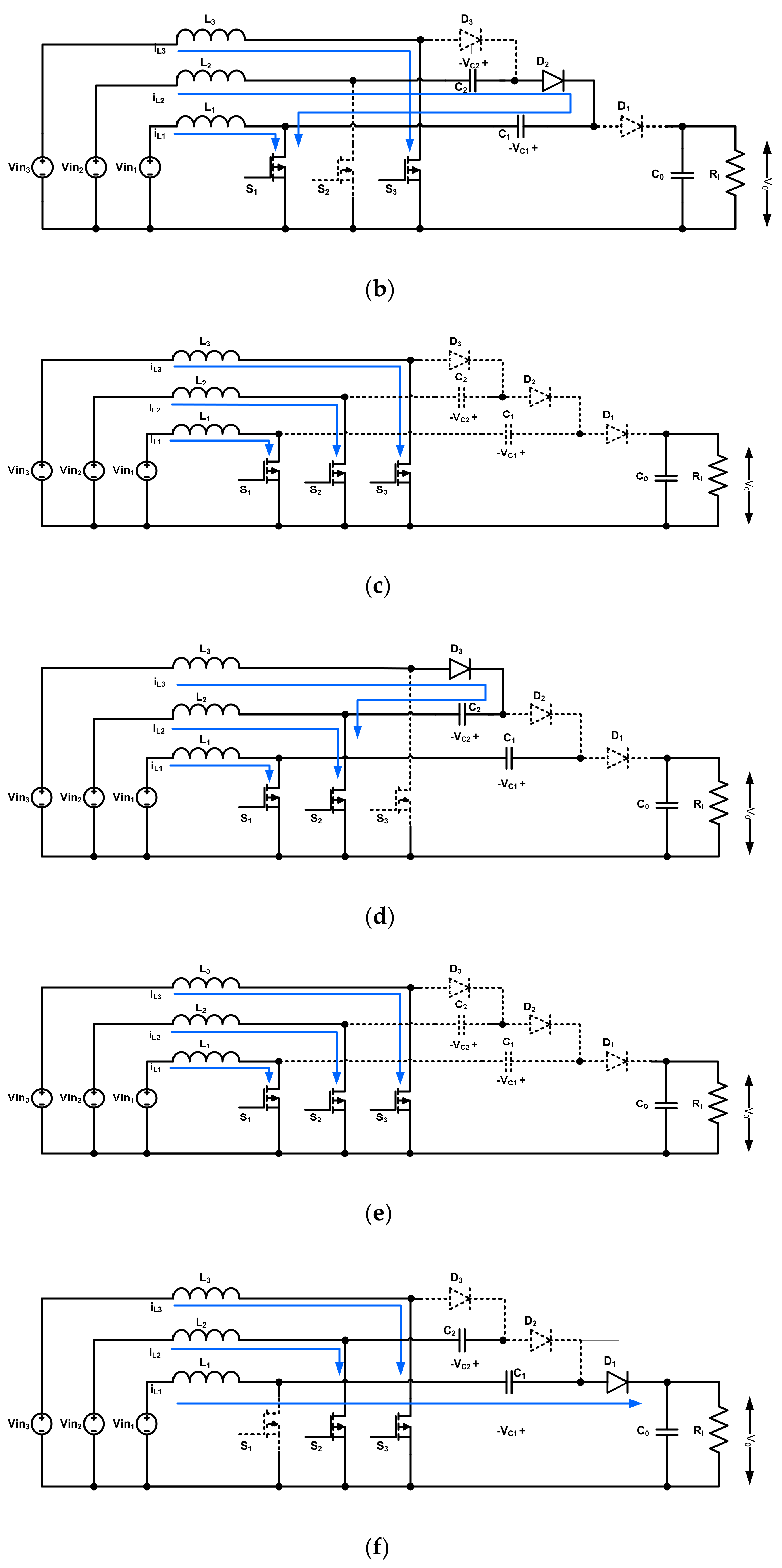
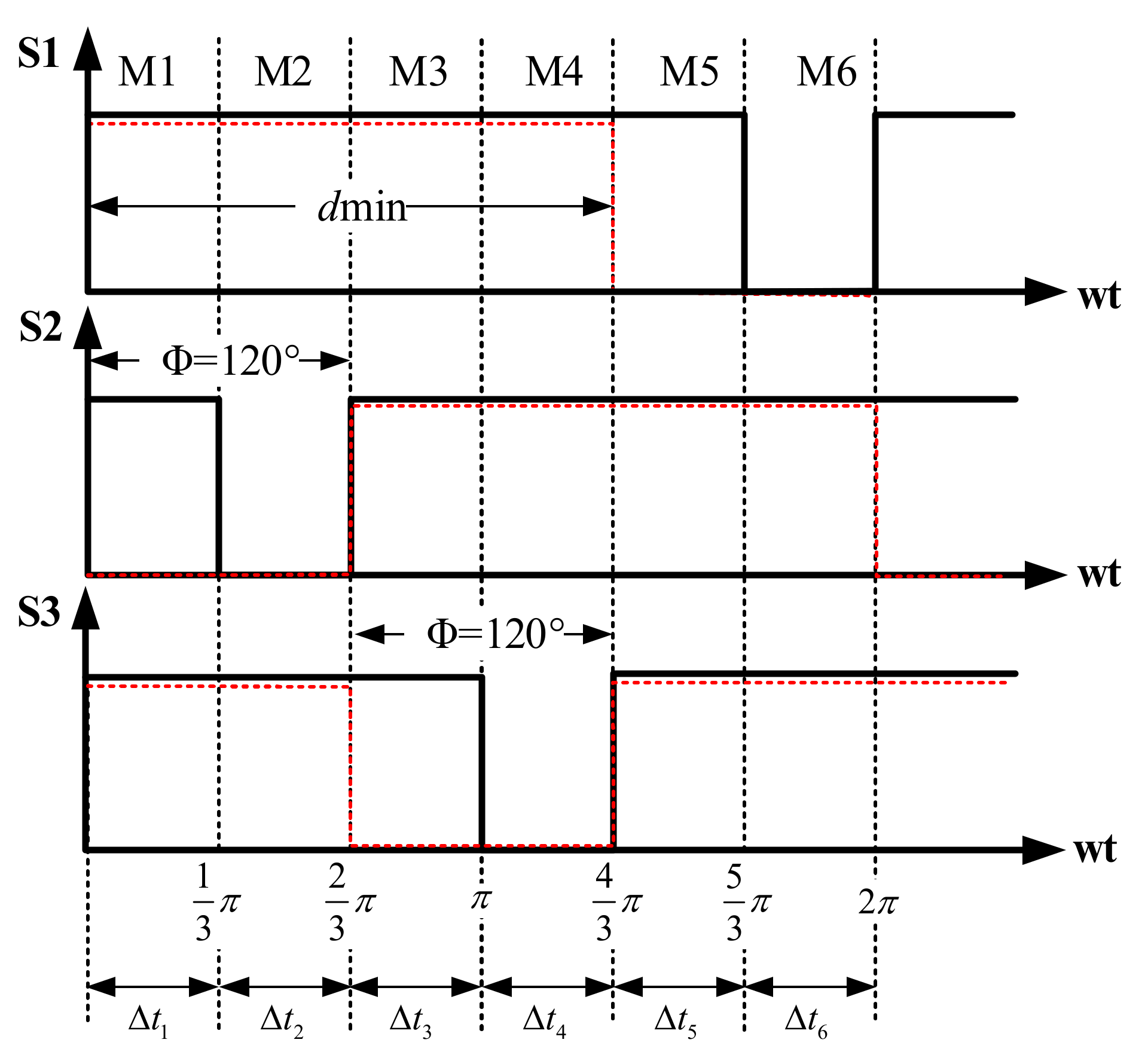
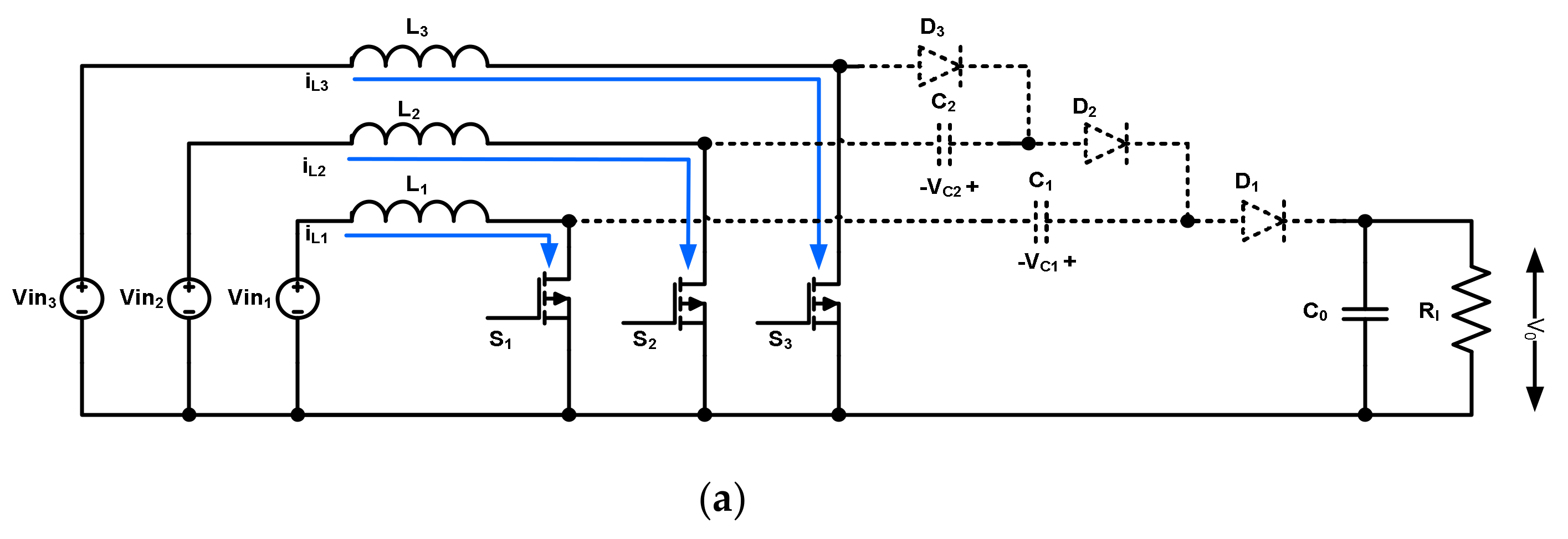
The converter analyzed in this paper is shown in Figure 1. It was first proposed in [13] for a low power application (100 W) for two inputs. The number of components is one MOSFET to each input source added; in this case, three input voltages are considered: Vin1, Vin2 and Vin3. Since the basic construction block is the boost converter, the only added component per input is a capacitor. To obtain the control switching signals, two basic conditions need to be considered: the phase shift in the control signals, φ = 360°/inputs = 360°/3 = 120°, and the minimum duty cycle, which is given by dmin = 1 − (1/inputs) = 0.66.

Figure 1.
Operating modes of the three-input step-up converter: (a) Mode 1, S1 = S2 = S3 = On, (b) Mode 2, S1 = S3 = On, S2 = Off, (c) Mode 3, S1 = S2 = S3 = On, (d) Mode 4, S1 = S2 = On, S3 = Off, (e) Mode 5, S1 = S2 = S3 = On, (f) Mode 6, S2 = S3 = On, S1 = On.
The six operating modes are shown in Figure 1. The control signals that generate these modes (M1 to M6) are presented in Figure 2. The control signals for dmin are indicated in red; it can be observed that, at any timeframe, there are two switches in conduction, at most.
Figure 2.
Control signals and operating modes in the three-input step-up converter.
To analyze the operation of each mode, the following initial conditions are considered: IL1, IL2 and IL3 currents are greater than zero, and C1 and C2 are charged to +VC1 and +VC2. The conditions in each operating mode are as follows:
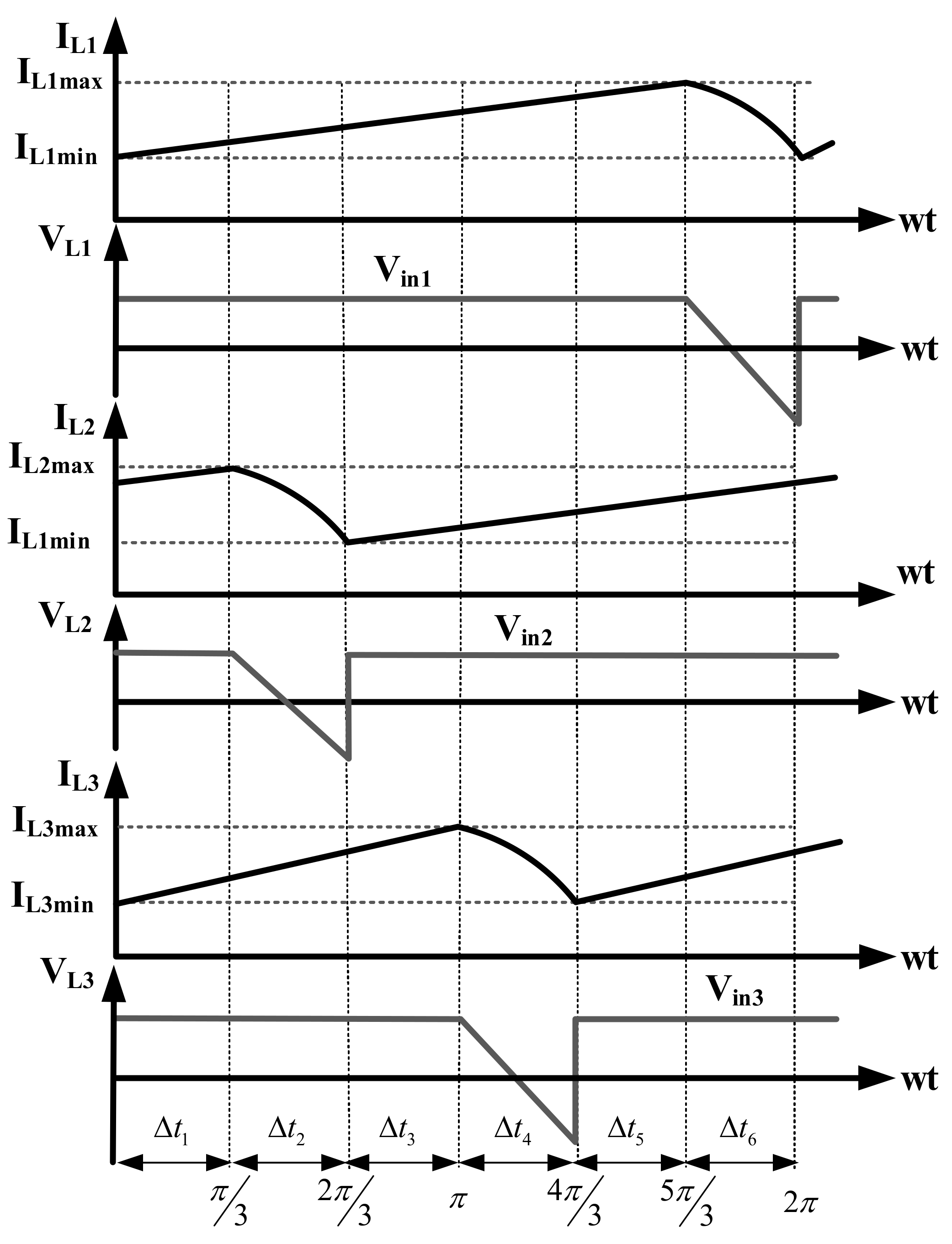
Mode 1, ∆t1 (see Figure 1a): This mode starts by turning on switches S1, S2 and S3 at the same timeframe; diodes D1, D2 and D3 are state–off. In this interval, inductors L1, L2 and L3 are charged by Vin1, Vin2 and Vin3, respectively. Currents IL1, IL2 and IL3 increase linearly from its minimum value to its maximum. Considering that the average currents through capacitor C1, C2 and Co are zero, voltages VC1, VC2 and VCo are constant. This mode ends when switch S2 is turned off at ∆t2.
Mode 2, ∆t2 (see Figure 1b). In this mode, S2 is turned off, and D2 is activated, allowing current of inductor L2 flows through C1 and C2. Thus, IL2 decreases linearly and charges C1 and C2, increasing their voltages. This mode ends when switch S2 is turned on at ∆t3.
Mode 4, ∆t4 (see Figure 1d). In this mode, S3 is turned off, and D3 is activated, allowing the current of inductor L3 flows through C2. Thus, IL3 decreases linearly and charges C2. This mode ends when switch S3 is gated ON at ∆t5.
Mode 6, ∆t6 (see Figure 1f). In this mode, S1 is turned off, and D1 is activated, allowing the current of inductor L1 flows through C1 and Co. Hence IL1 decreases linearly and begins to charge Co; at the same timeframe, C1 is discharged to RL. This mode ends when switch S1 is gated ON.
Although modes 1, 3 and 5 are the same, they are shown for completeness.
Converter stationary ideal waveforms obtained from analysis of its six operation modes are qualitative depicted in Figure 3.
Figure 3.
Ideal waveforms of three-input step-up converter.
Model Based on a State Variable Equations
To obtain a model of the converter based on the state space analysis, the state variables are chosen according to:
According to the procedure described in [12], the state space equations for the six operating modes are shown in Table 1.
Table 1.
State space equations.
Let us introduce the notation for every switch state:
Then, the following general state space representation can be obtained:
3. Design Procedure and Simulation Results
Although the converter uses three different input voltages, components are designed considering the lowest voltage, Vin min; due to inductors, current is maximum under this condition.
The complete development of the converter design equations was derived in [12] for the two-input case. Generalization of these equations was obtained from the operating modes described in the previous section. The gain for a three-input converter, MVDC, is:
where d is the duty cycle of switching devices operation, and Iinn is the input current for each source. The duty cycle is determined according to an open loop control, where the output power or the voltage gain, MVDC, are specified. To calculate inductance values, note that the inputs of the converter are the same as the conventional boost converter, hence:
where is the ripple current of inductor, and is the switching frequency.
Capacitors C1 and C2 were carefully designed, since a small value may generate an inadequate conversion ratio, and a very large value will affect the time response and create output voltage oscillations. Note that voltage on capacitors C1 and C2 affect the output voltage only through inductor currents. This can be observed from state equations, particularly from the output voltage equation; the output voltage derivative only depends on the output voltage, itself, the current x1, the load and the output capacitor. Hence, ripple voltage in these capacitors can have a wide range, since this ripple is not reflected at the converter output. As it is proved in [12], the capacitors can be calculated according to:
where Io is the output current and are the ripple voltage of C1, C2 and Co respectively.
The converter output voltage is given by:
Using Equations (10)–(13), the final component values are obtained and listed in Table 2, together with the design conditions. A simulation was performed in Saber™ using ideal components to validate the design procedure and the correct operation of the three-input step-up converter.
Table 2.
Test parameters and components.
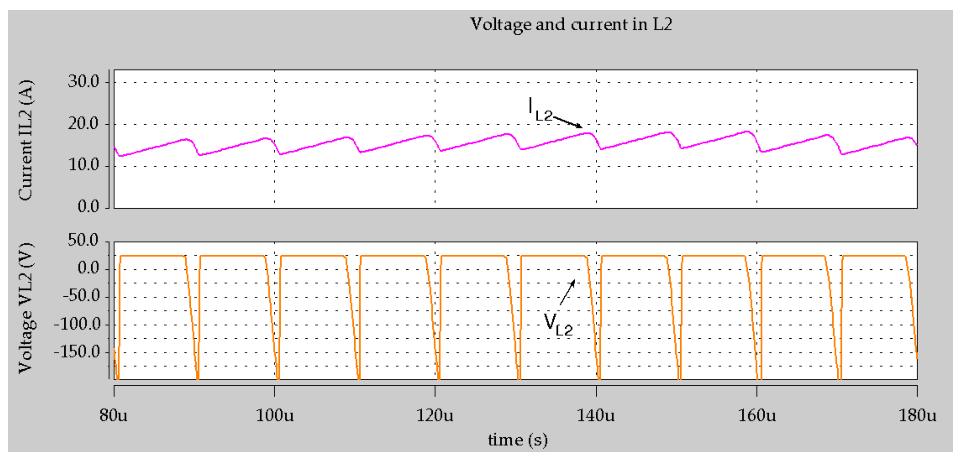
Control signals S1, S2 and S3 are shown in Figure 4 with a phase shift φ = 120° and d = 0.72 The voltages VL1, VL2 and VL3 and currents IL1, IL2 and IL3 are shown in Figure 5, Figure 6 and Figure 7, respectively. They can be contrasted with the ideal waveforms of Figure 3 to verify the correct operation of the converter.
Figure 4.
Simulation results for digital control signal S1, S2, S3 with φ = 120° and d = 0.72.
Figure 5.
Simulation results for IL1 and VL1.
Figure 6.
Simulation results for IL2 and VL2.
Figure 7.
Simulation results for IL3 and VL3.
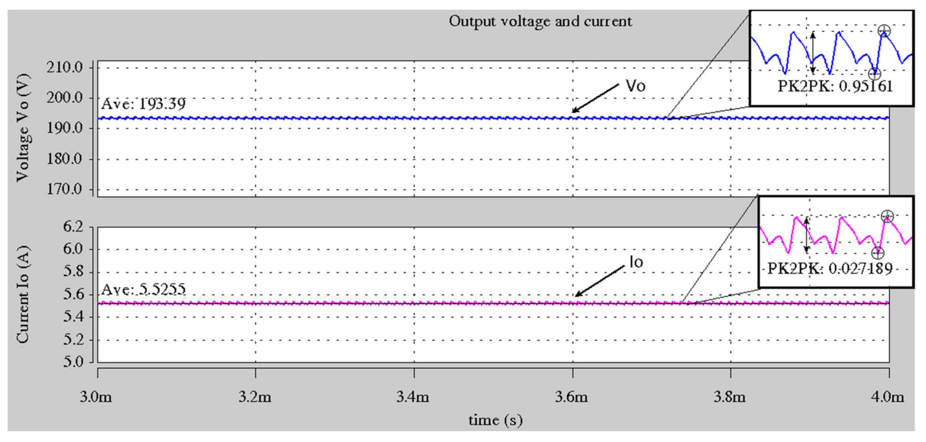
Simulation results for output voltage and current, Vo and Io are shown in Figure 8 with DC (average) values VODC = 193.39 V and IODC = 5.52 A, getting an output power of Po = 1.067 kW. The ripple voltage obtained ΔVo = 951 mV.
Figure 8.
Simulation results for Vo and Io.
4. Experimental Results
Considering that the maximum drain-source voltage is the output voltage, SiC transistors CMF20120 and diodes C3 D06060 were employed to reduce switching losses in the implemented prototype. The NXP TWR−KV 58 F220 microcontroller was used to generate the PWM pulses with a phase shifted of 120°. Inductors were designed and constructed, following the methodology presented in [14].
The efficiency of the converter is determined by:
The measure input current values were:
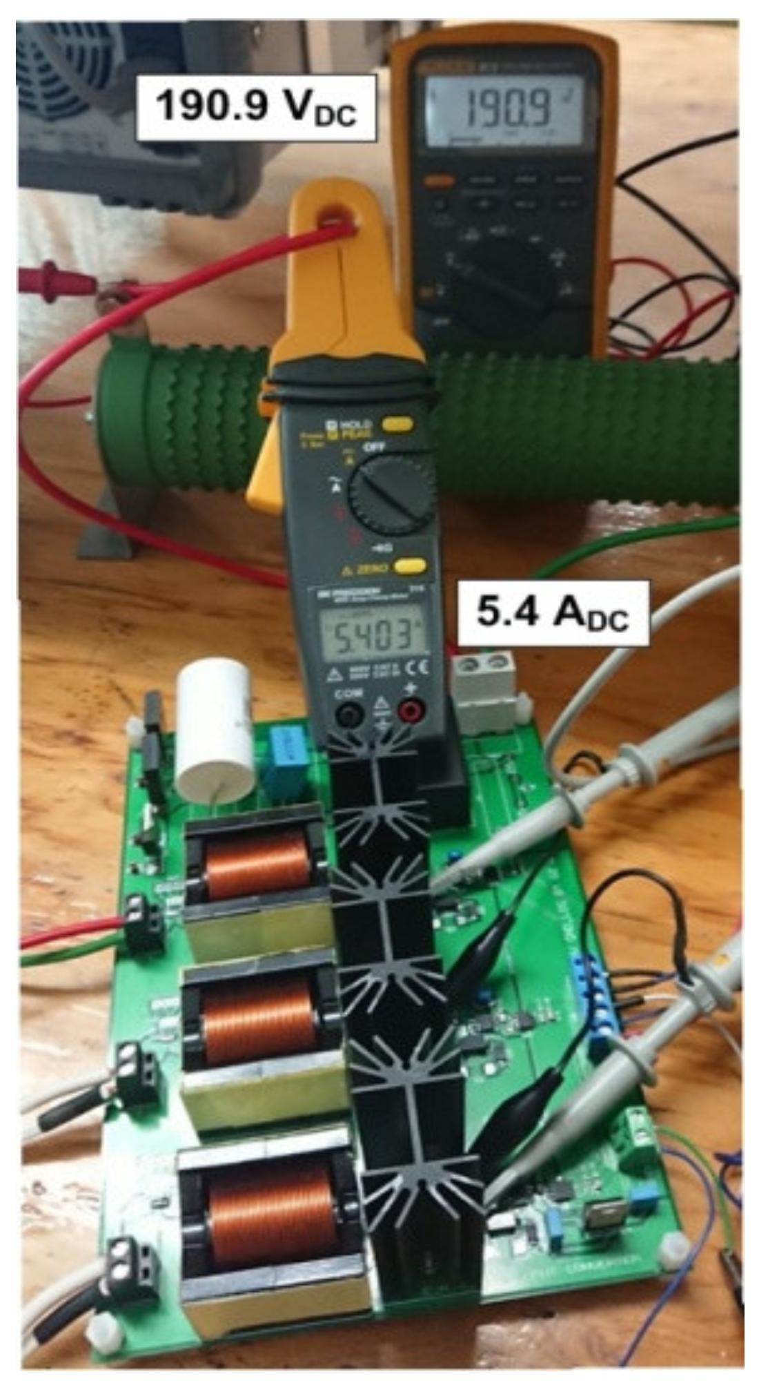
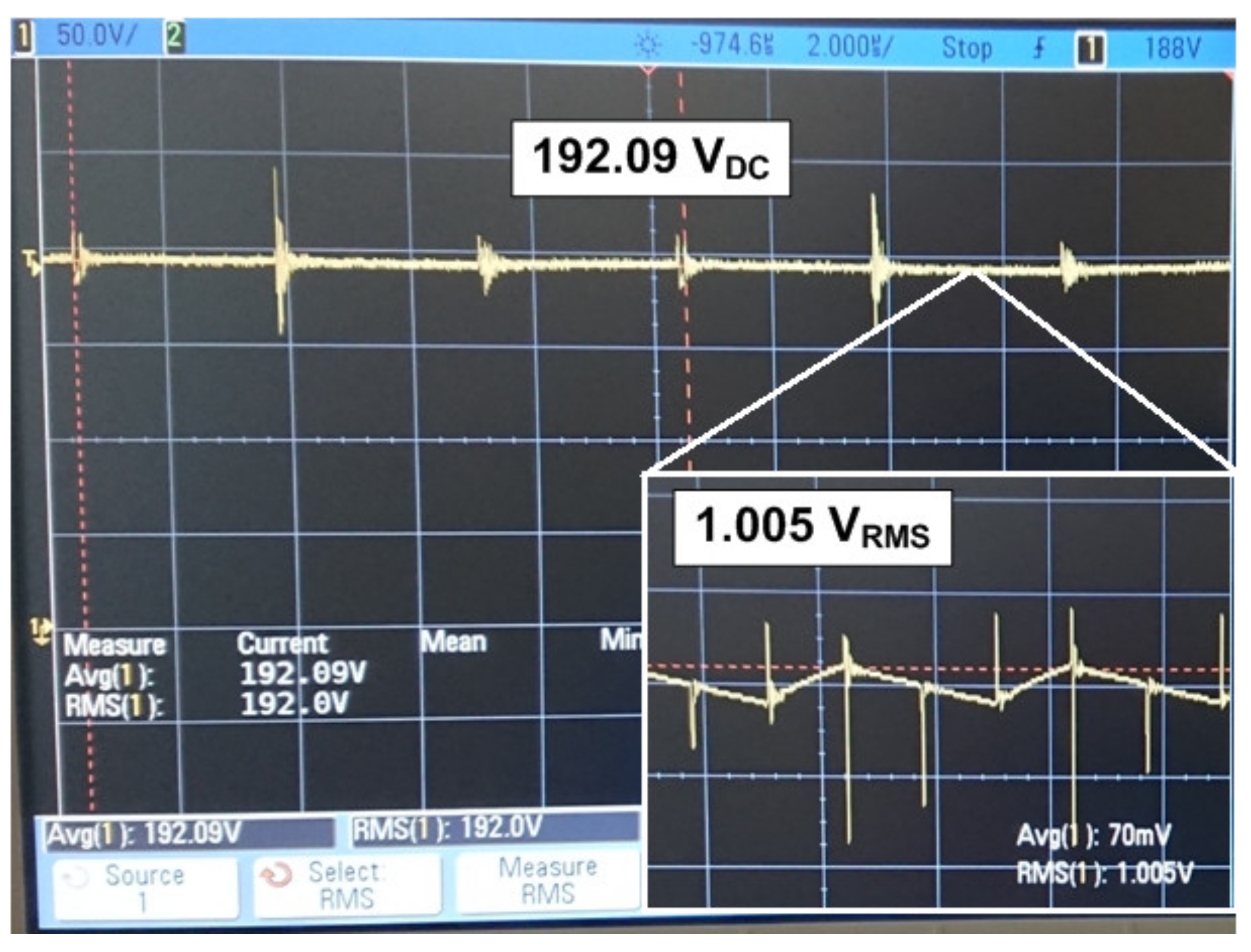
The implemented prototype can be seen in Figure 9, where the main components are indicated. Output voltage and current are shown in Figure 10; obtained multimeter measurements are 190.9 VDC and 5.4 ADC. In Figure 11, it can be seen that the output voltage is 192.09 VDC, with ripple voltage of 1.005 VRMS, resulting in an output power of Po = 1.037 kW.
Figure 9.
Implemented 1 kW prototype.
Figure 10.
Implemented 1 kW prototype with voltage and current measurement.
Figure 11.
Experimental results Vo = 192.09 VDC, ΔVo = 1.005 V.
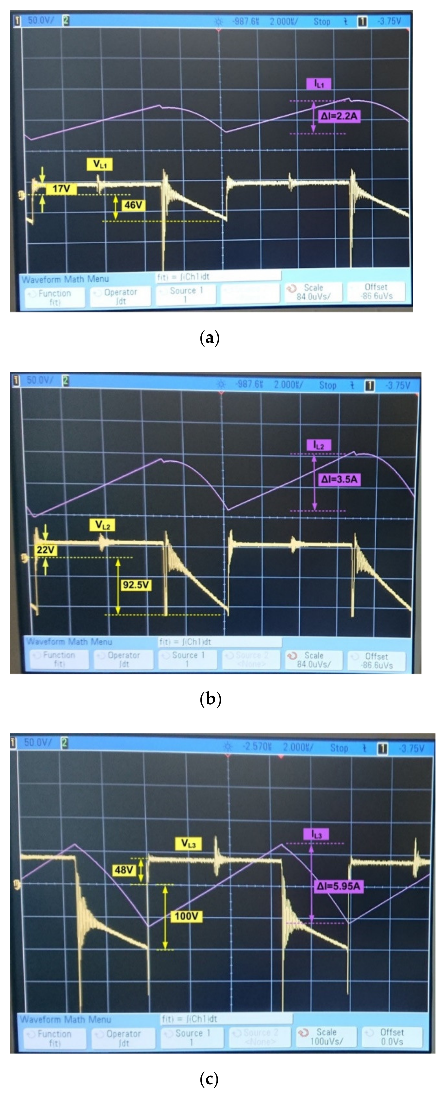
In Figure 12, voltage and current waveforms of inductors L1, L2 and L3 are shown. Positive amplitudes in voltage waveforms are approximately equal to the value of the corresponding input voltage supply. A comparison of these waveforms with the ideal waveforms of Figure 3 and Figure 5, Figure 6, Figure 7, Figure 8 shows their similarity, validating the experimental results. Spikes and high-amplitude ripples observed in the experimental waveforms show the existence of parasitic components that are not considered in simulation.
Figure 12.
Experimental results: (a) VL1 and IL1, input voltage Vin1 = 12 V, (b) VL2 and IL2, input voltage Vin2 = 24 V, (c) VL3 and IL3, input voltage Vin2 = 48 V.
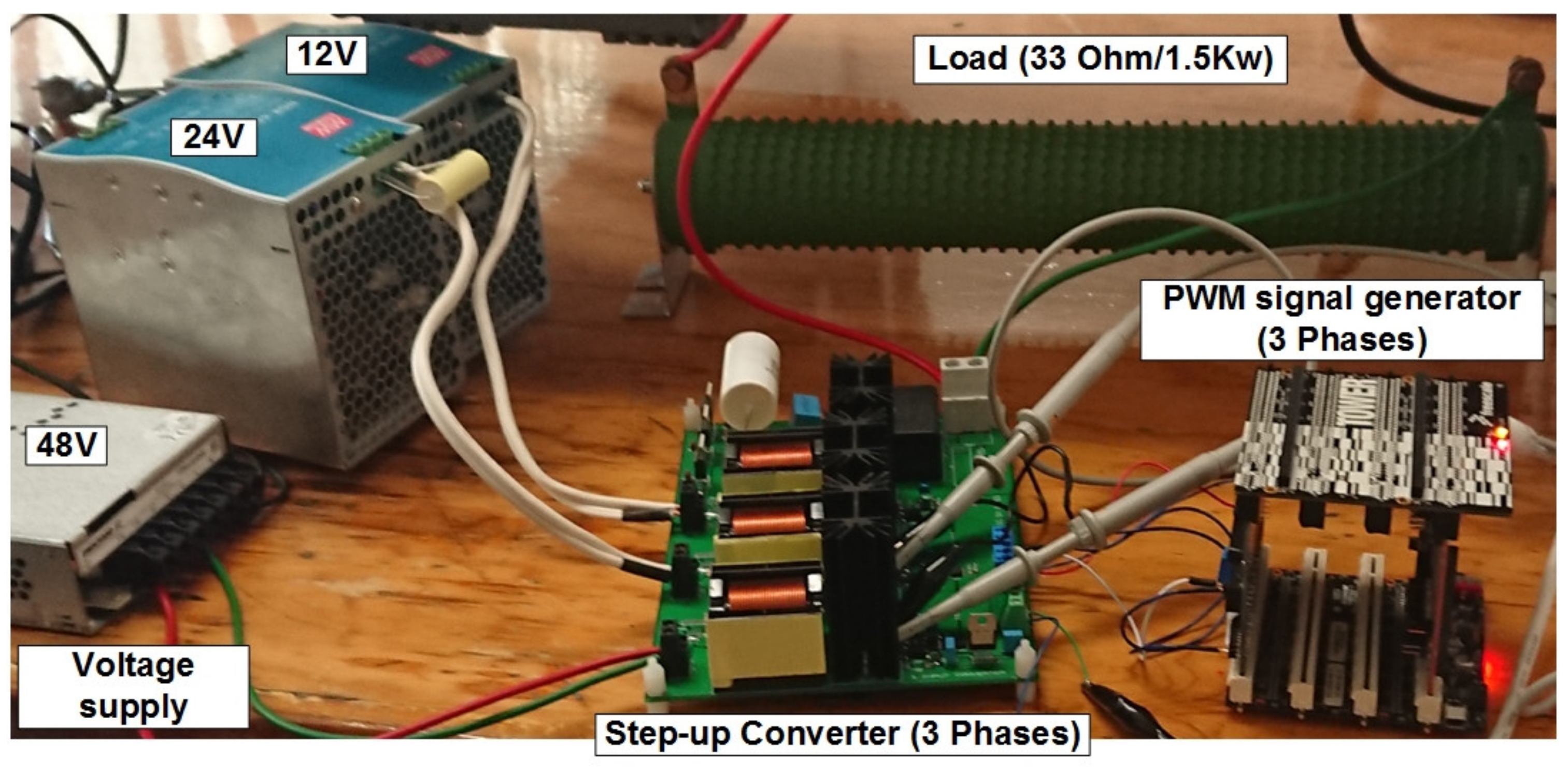
According to Equation (15), and using the input voltages and currents, the efficiency obtained is η = 90.51%. Figure 13 shows the experimental set up: (a) three-input step-up converter, (b) three input voltage sources, (c) the PWM signal generator and (d) the 33 Ω output load.
Figure 13.
Experimental prototype with three input voltage sources, 33 Ω output load and the PWM signal generator.
A comparison between the proposed converter and similar topologies is summarized in Table 3. The implemented converter provides the highest output power, keeping a high efficiency, considering three voltage sources in its design. The number of energy storage elements is less than the converters proposed in [9,10,11,12,15,16]. The high switching frequency (100 kHz) is a factor to reduce its implementation size.
Table 3.
A comparison between the proposed converter and similar topologies.
5. Conclusions
A high-gain three-input step-up converter of 1 kW was analyzed, designed and implemented. The design procedure was validated through experimental results. In addition, the converter efficiency and reliability were verified, obtaining a power of 1037 W, with an efficiency of 90.51%, which is superior to similar proposals. The converter topology can be used for a wide range of applications; in particular, the topology could be used as a low-cost alternative to jointly use several renewable sources that may be backed up by a nonrenewable source, allowing the prioritization of power sources at any time. Based on the obtained results, it can be said that the converter topology can be used for higher powers and more inputs.
Author Contributions
Conceptualization, E.N.-H., L.H.-G. and D.C.; data curation, J.R.-H. and D.C.; formal analysis, L.H.-G., D.C. and J.R.-H.; funding acquisition, E.N.-H. and L.H.-G.; investigation, E.N.-H., L.H.-G., D.C. and J.R.-H.; methodology, E.N.-H. and L.H.-G.; project administration, L.H.-G.; resources, D.C. and J.R.-H.; software, E.N.-H., L.H.-G. and J.R.-H.; supervision, L.H.-G. and D.C.; validation, E.N.-H. and L.H.-G.; visualization, E.N.-H. and L.H.-G.; writing, original draft, E.N.-H. and L.H.-G.; writing, review and editing, D.C. and J.R.-H. All authors have read and agreed to the published version of the manuscript.
Funding
This research was funded by Instituto Politécnico Nacional.
Acknowledgments
The authors are grateful to the Instituto Politécnico Nacional (IPN) for their encouragement and kind economic support to realize the research project.
Conflicts of Interest
The authors declare no conflict of interest.
Nomenclature
| Vin1, Vin2, Vin3 | Three input voltages |
| Φ | Control signals phase shift |
| d | Duty cycle in switching devices |
| dmin | Minimum duty cycle |
| S1, S2, S3 | Digital control signals in each transistor |
| L1, L2, L3 | Inductors for each input voltage source |
| IL1, IL2, IL3 | Currents in inductor L1, L2 and L3 |
| ΔI1, ΔI2, ΔI3 | Ripple current in L1, L2 and L3 |
| C1, C2 | Capacitors in boost circuits in first and second inputs |
| VC1, VC2 | Voltage in capacitors C1 and C2 |
| D1, D2, D3 | Diodes in boost circuits for each input |
| Co | Output capacitor |
| Vo | Output DC voltage |
| RL | Output load |
| ∆t1 to ∆t6 | Time interval in each operating mode |
| M1 to M6 | Operating modes 1 to 6 |
| x1 to x6 | State variables in state space analysis |
| Vin min | Minimum input voltage |
| MVDC | Voltage gain |
| fs | Switching frequency |
| swn, n = 1, 2, 3 | State of switches S1, S2 and S3 |
| Io | Output current |
| ΔVc1, ΔVc2 | Ripple voltage in C1 and C2 |
| Vo | Output voltage |
| ΔVo | Output voltage ripple |
| Po | Output power |
| Pin1, Pin2, Pin3 | Input power for each voltage source |
| η | Converter efficiency |
References
- Prasanth, J.; Rajasekar, N. A Novel Flower Pollination Based Global Maximum Power Point Method for Solar Maximum Power Point Tracking. IEEE Trans. Power Electron. 2015, 32, 8486–8499. [Google Scholar] [CrossRef]
- Yaramasu, V.; Dekka, A.; Durán, M.; Kouro, S.; Wu, B. PMSG-based wind energy conversion systems: Survey on power converters and controls. IET Electr. Power Appl. 2017, 11, 956–968. [Google Scholar] [CrossRef]
- Teng, Y.; Wang, Z.; Li, Y.; Ma, Q.; Hui, Q.; Li, S. Multi-energy storage system model based on electricity heat and hydrogen coordinated optimization for power grid flexibility. CSEE J. Power Energy Syst. 2019, 5, 266–274. [Google Scholar]
- Liu, Y.-C.; Chen, Y.-M. A Systematic Approach to Synthesizing Multi-Input DC–DC Converters. IEEE Trans. Power Electron. 2009, 24, 116–127. [Google Scholar] [CrossRef]
- Chew, Z.J.; Ruan, T.; Zhu, M. Power Management Circuit for Wireless Sensor Nodes Powered by Energy Harvesting: On the Synergy of Harvester and Load. IEEE Trans. Power Electron. 2018, 34, 8671–8681. [Google Scholar] [CrossRef]
- Pooranian, Z.; Abawajy, J.H.; Vinod, P.; Mauro, C. Scheduling Distributed Energy Resource Operation and Daily Power Consumption for a Smart Building to Optimize Economic and Environmental Parameters. Energies 2018, 11, 348. [Google Scholar] [CrossRef]
- Zhang, Y.; He, J.; Ionel, D.M. Modelling and Control of a Multiport Converter based EV Charging Station with PV and Battery. In Proceedings of the IEEE Transportation Electrification Conference, Detroit, MI, USA, 1–5 June 2019. [Google Scholar]
- Schumacher, D.; Beik, O.; Emadi, A. Standalone Integrated Power Electronics System: Applications for Off-Grid Rural Locations. IEEE Electrif. Mag. 2018, 6, 73–82. [Google Scholar] [CrossRef]
- Mohseni, P.; Hossein, H.S.; Sabahi, M.; Jalilzadeh, T.; Maalandish, M. A New High Step-Up Multi-Input Multi-Output DC–DC Converter. IEEE Trans. Ind. Electron. 2019, 66, 5197–5208. [Google Scholar] [CrossRef]
- Faraji, R.; Farzanehfard, H.; Kampitsis, G.; Mattavelli, M.; Matioli, E.; Esteki, M. Fully Soft-Switched High Step-Up Nonisolated Three-Port DC–DC Converter Using GaN HEMTs. IEEE Trans. Ind. Electron. 2010, 67, 8371–8380. [Google Scholar] [CrossRef]
- Varesi, K.; Hossein, H.S.; Sabahi, M.; Babaei, E. Modular non-isolated multi-input high step-up dc–dc converter with reduced normalised voltage stress and component count. IET Power Electron. 2018, 11, 1092–1100. [Google Scholar] [CrossRef]
- Netzahuatl, E.; Cortes, D.; Ramirez-Salinas, M.A.; Resa, J.; Hernandez, L.; Hernandez, F.D. Modeling, Design Procedure and Control of a Low-Cost High-Gain Multi-Input Step-Up Converter. Electronics 2019, 8, 424. [Google Scholar] [CrossRef]
- Zhou, L.; Zhu, B.; Luo, Q. High step-up converter with capacity of multiple input. IET Power Electron. 2012, 5, 524–531. [Google Scholar] [CrossRef]
- McLyman, C.W.T. Transformer and Inductor Design Handbook; CRC Press: Boca Raton, FL, USA, 2017; ISBN 9781439836880. [Google Scholar]
- Varesi, K.; Hossein, H.S.; Sabahi, M.; Babei, E.; Vosoughi, N. Performance and design analysis of an improved non-isolated multiple input buck DC–DC converter. IET Power Electron. 2017, 10, 1034–1045. [Google Scholar] [CrossRef]
- Sun, Z.; Bae, S. Multiple-input Soft-switching Ćuk Converter. In Proceedings of the IEEE Energy Conversion Congress and Exposition, Cincinnati, OH, USA, 1–5 October 2017. [Google Scholar]
Publisher’s Note: MDPI stays neutral with regard to jurisdictional claims in published maps and institutional affiliations. |
© 2021 by the authors. Licensee MDPI, Basel, Switzerland. This article is an open access article distributed under the terms and conditions of the Creative Commons Attribution (CC BY) license (http://creativecommons.org/licenses/by/4.0/).