
Analysis of a DC-DC Flyback Converter Variant for Thermoelectric Generators with Partial Energy Processing

 ,
, 
 ,
,  ,
,  , ,
, ,  and
and
Abstract
1. Introduction
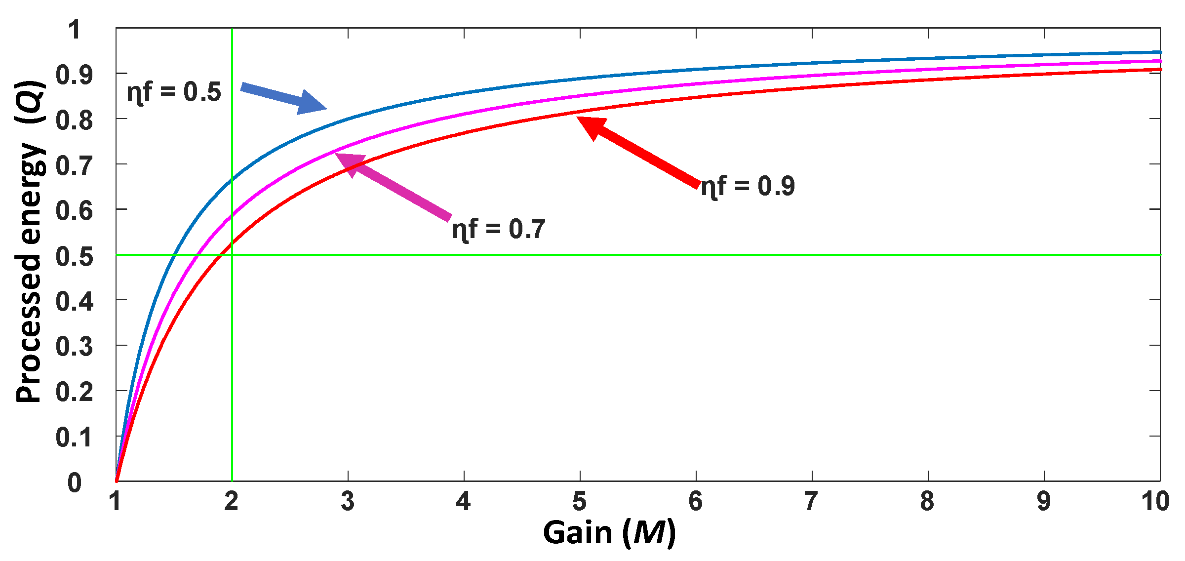
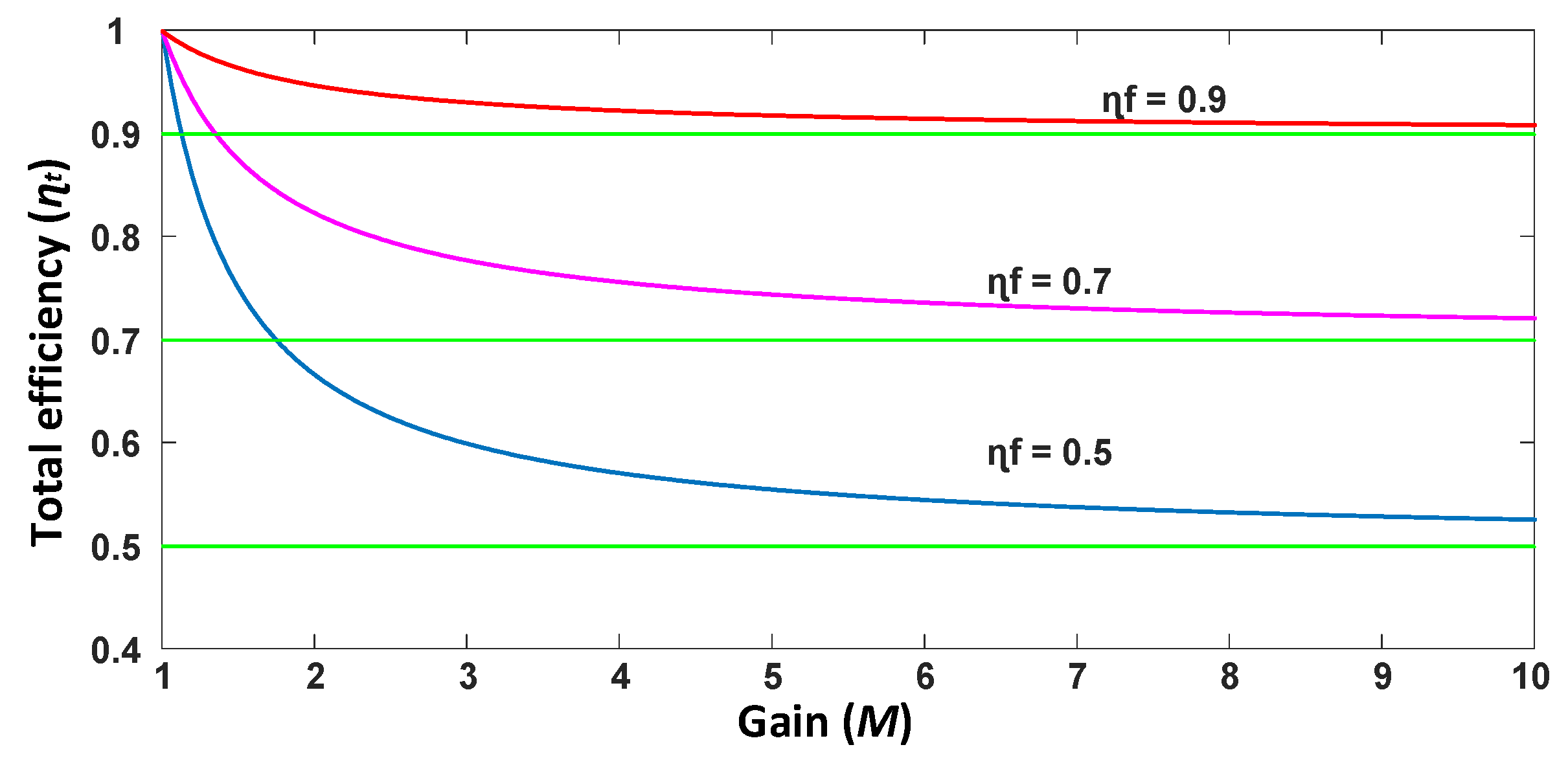
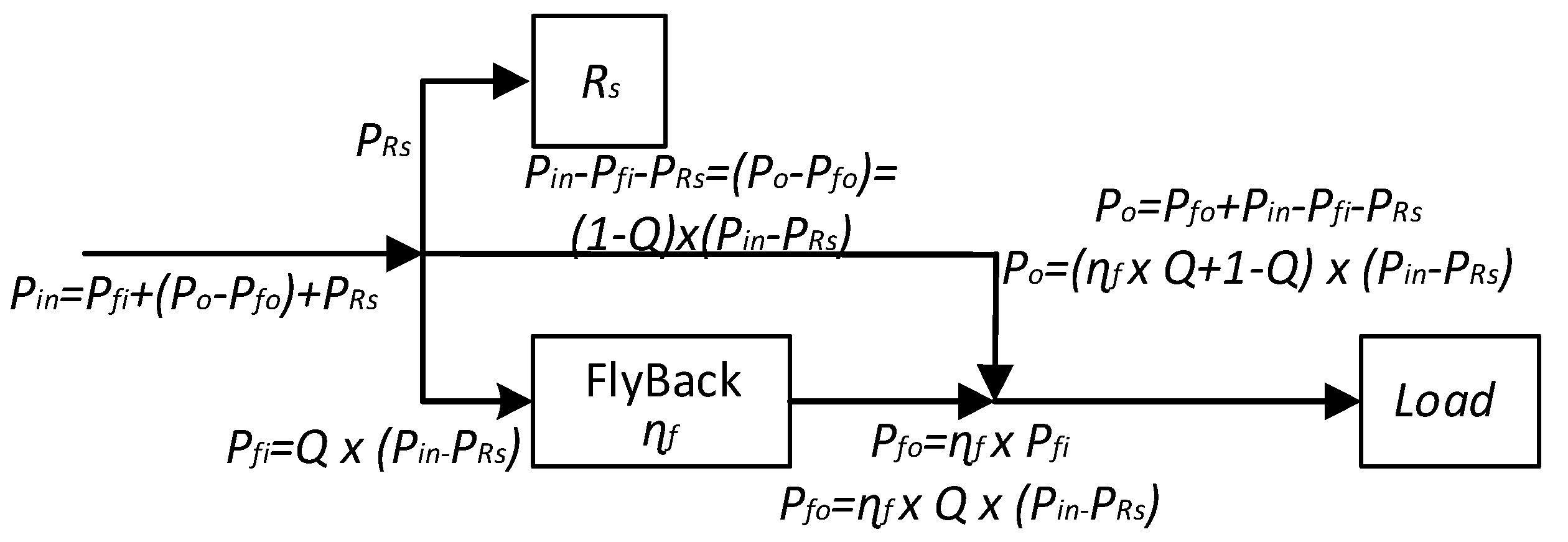
2. Analysis of the Flyback Converter
2.1. Without Internal Resistance in the Source
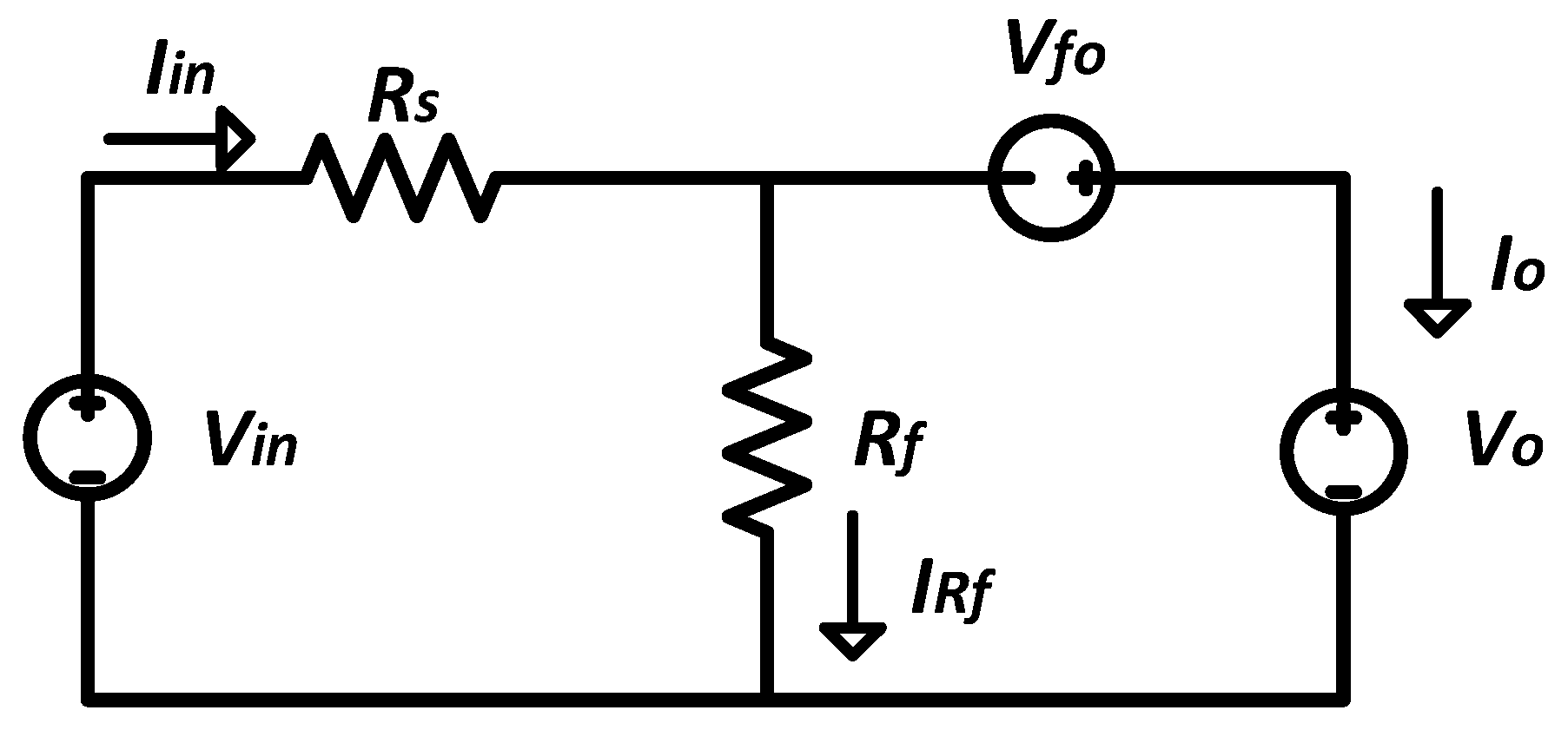
2.2. With Internal Resistance in the Source
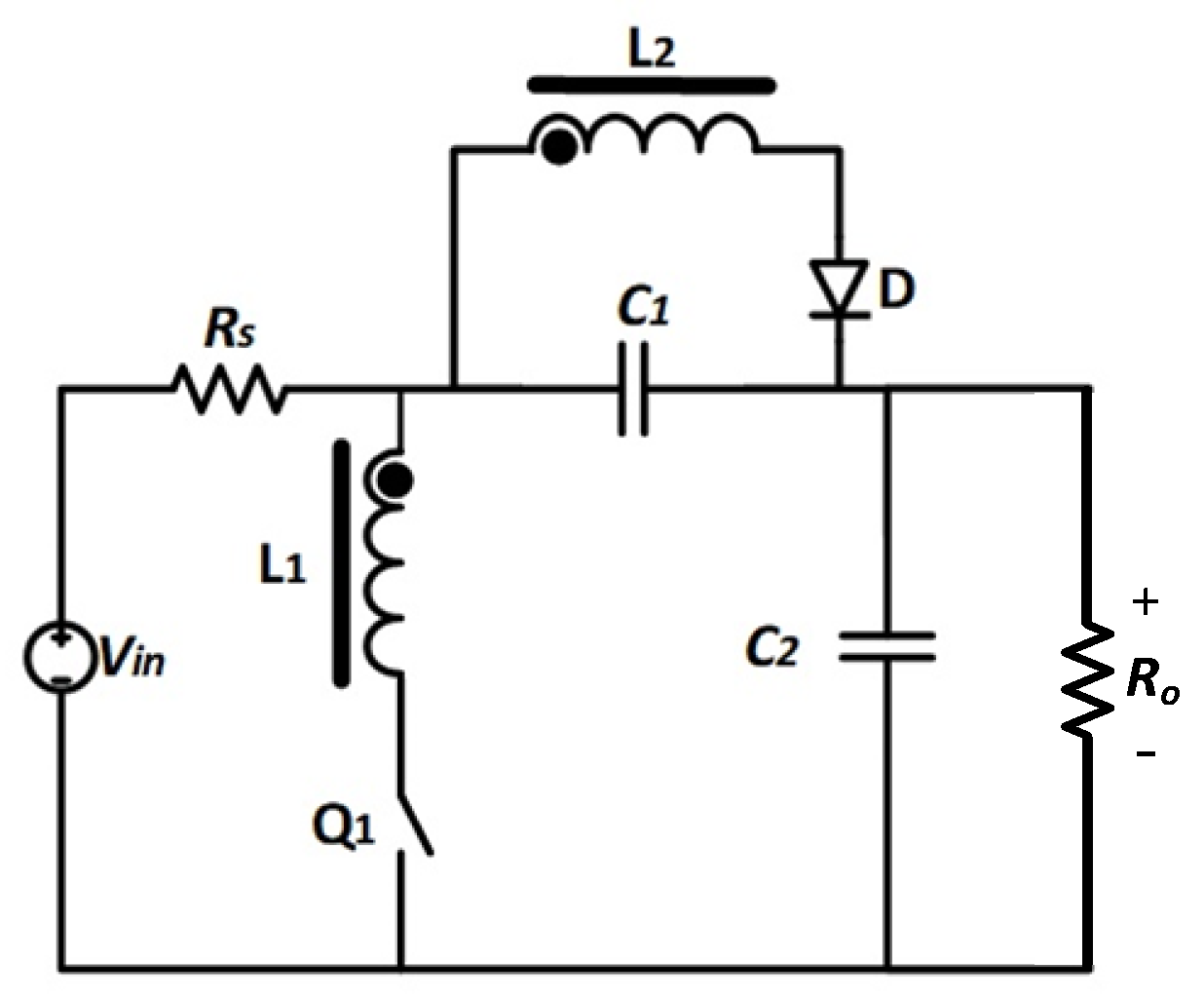
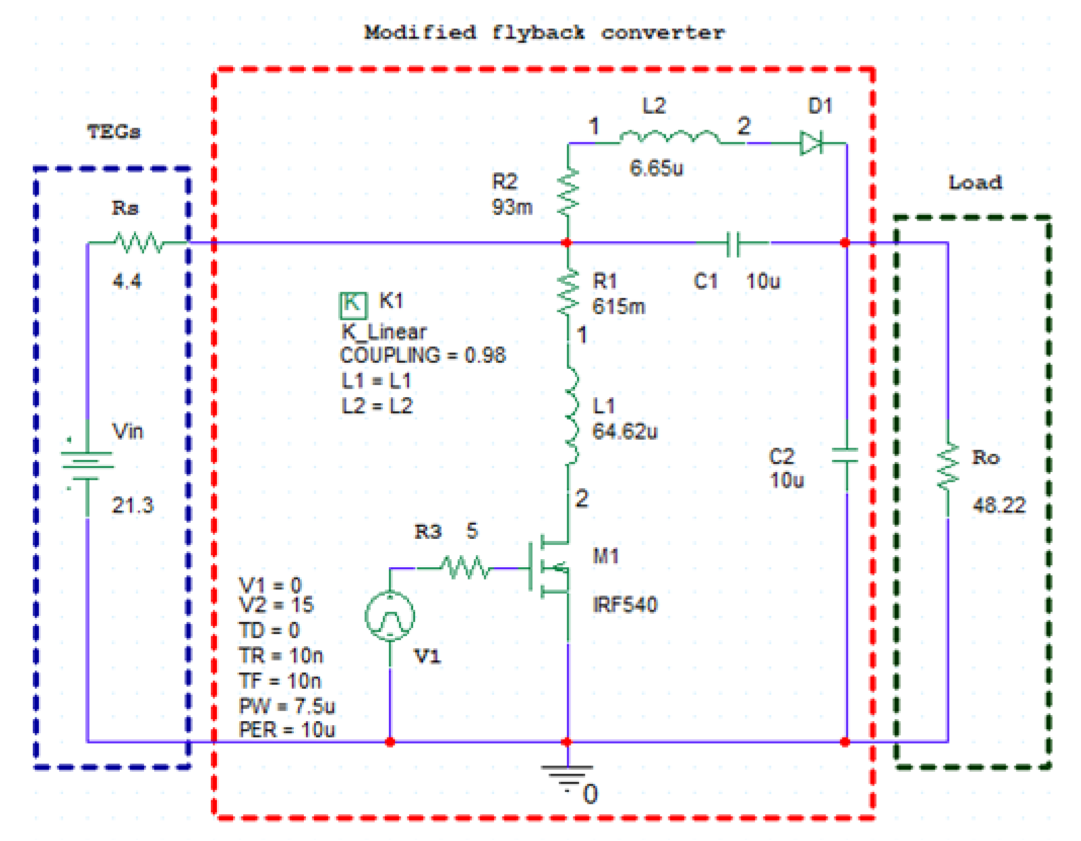
3. Design of the Rearranged Flyback Converter
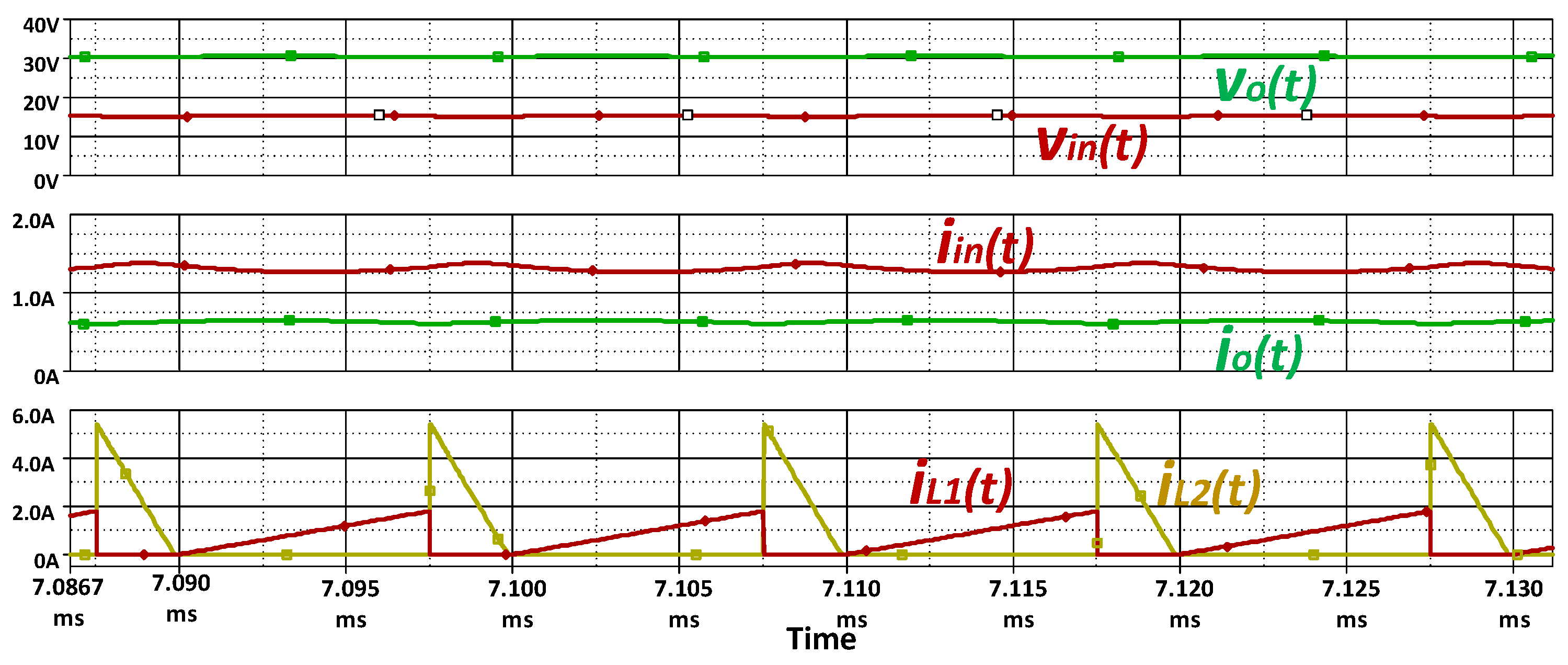
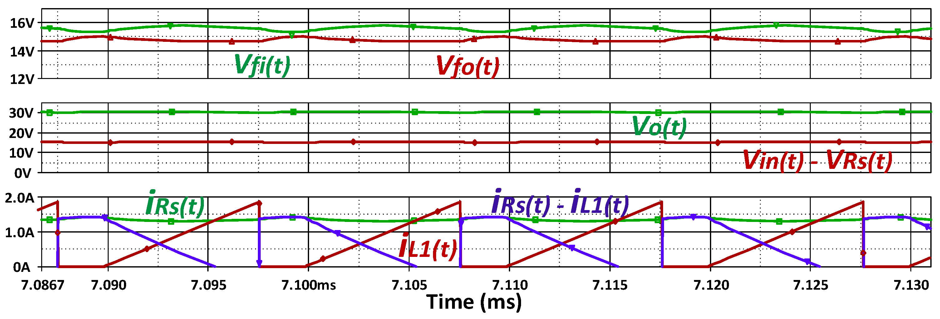
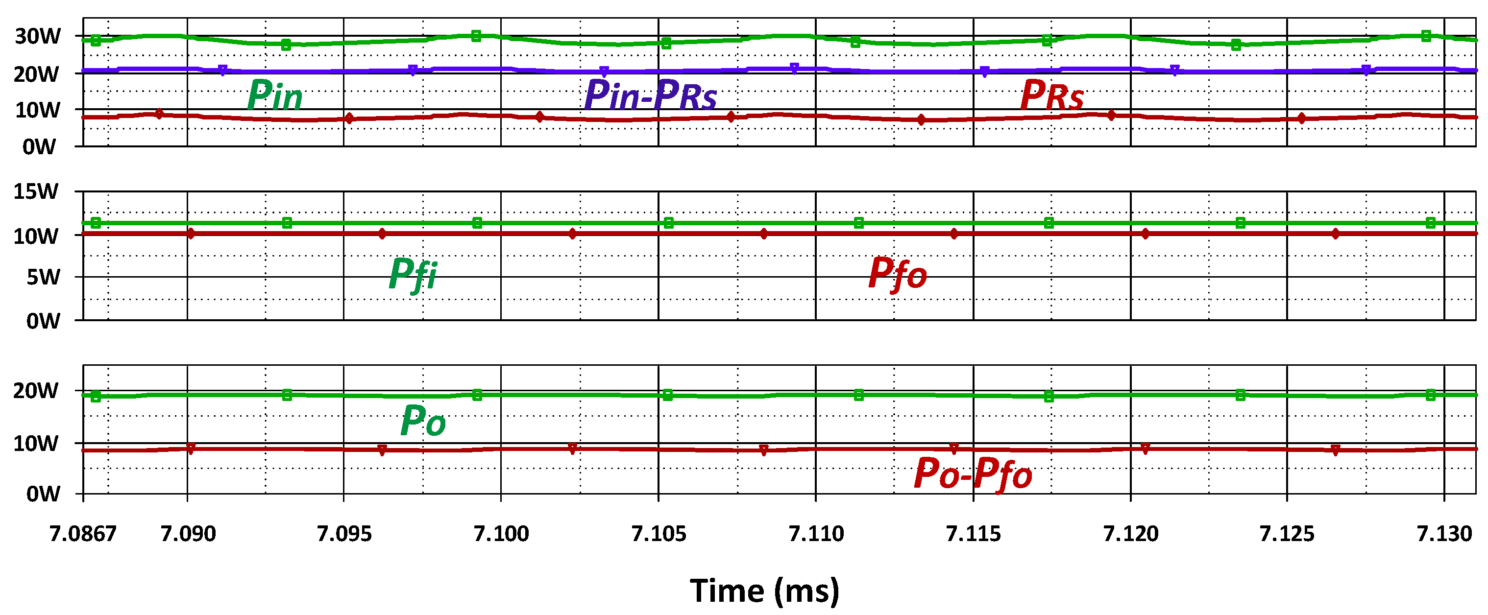
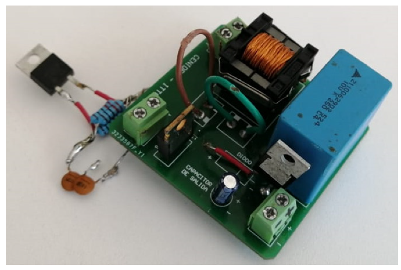
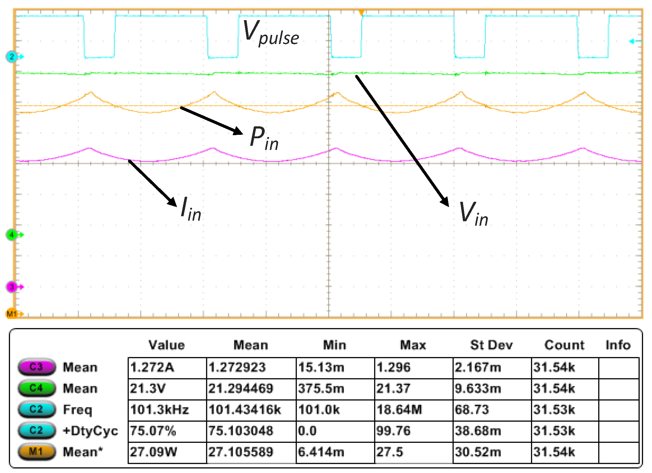
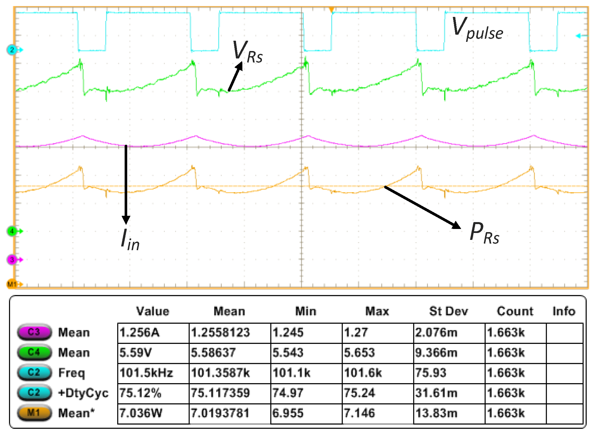
4. Experimental Results
5. Conclusions
Author Contributions
Funding
Conflicts of Interest
References
- Lv, S.; He, W.; Jiang, Q.; Hu, Z.; Liu, X.; Chen, H.; Liu, M. Study of different heat exchange technologies influence on the performance of thermoelectric generators. Energy Convers. Manag. 2018, 156, 167–177. [Google Scholar] [CrossRef]
- Sudharshan, K.; Kumar, V.P.; Barshilia, H.C. Performance evaluation of a thermally concentrated solar thermo-electric generator without optical concentration. Sol. Energy Mater. Sol. Cells 2016, 157, 93–100. [Google Scholar] [CrossRef]
- Maran, A.L.O.; Henao, N.C.; Silva, E.A.; Schaeffer, L.; Junior, O.H.A. Use of the Seebeck Effect for Energy Harvesting. IEEE Lat. Am. Trans. 2016, 14, 4106–4114. [Google Scholar] [CrossRef]
- Datas, A.; Martí, A. Thermophotovoltaic energy in space applications: Review and future potential. Sol. Energy Mater. Sol. Cells 2017, 161, 285–296. [Google Scholar] [CrossRef]
- Cao, Q.; Luan, W.; Wang, T. Performance enhancement of heat pipes assisted thermoelectric generator for automobile exhaust heat recovery. Appl. Therm. Eng. 2018, 130, 1472–1479. [Google Scholar] [CrossRef]
- Kumar, T.K.; Kumar, S.A.; Ram, K.K.; Goli, K.R.; Prasad, V.S. Analysis of thermo electric generators in automobile applications. Mater. Today Proc. 2020. [Google Scholar] [CrossRef]
- Sornek, K.; Filipowicz, M.; Żołądek, M.; Kot, R.; Mikrut, M. Comparative analysis of selected thermoelectric generators operating with wood-fired stove. Energy 2019, 166, 1303–1313. [Google Scholar] [CrossRef]
- Dalala, Z.M.; Hamdan, Z.S.; Al-Taani, H.; Al-Addous, M.; Albatayneh, A. Battery Charging Application with Thermoelectric Generators as Energy Harvesters. Acad. Res. Community Publ. 2019, 3, 248. [Google Scholar] [CrossRef]
- Ebling, D.G.; Krumm, A.; Pfeiffelmann, B.; Gottschald, J.; Bruchmann, J.; Benim, A.C.; Ádám, M.; Labs, R.; Herbertz, R.R.; Stunz, A. Development of a System for Thermoelectric Heat Recovery from Stationary Industrial Processes. J. Electron. Mater. 2016, 45, 3433–3439. [Google Scholar] [CrossRef]
- Francioso, L.; De Pascali, C.; Sglavo, V.; Grazioli, A.; Masieri, M.; Siciliano, P. Modelling, fabrication and experimental testing of an heat sink free wearable thermoelectric generator. Energy Convers. Manag. 2017, 145, 204–213. [Google Scholar] [CrossRef]
- Ma, Q.; Fang, H.; Zhang, M. Theoretical analysis and design optimization of thermoelectric generator. Appl. Therm. Eng. 2017, 127, 758–764. [Google Scholar] [CrossRef]
- Yu, H.; Chen, M.; Wu, C.; Tang, K.-T.; Wang, G. A batteryless and single-inductor DC-DC boost converter for thermoelectric energy harvesting application with 190mV cold-start voltage. In Proceedings of the 2018 IEEE International Symposium on Circuits and Systems (ISCAS), Florence, Italy, 27–30 May 2018; pp. 1–4. [Google Scholar]
- Moreno, J.M.; Vazquez, A.S.M.; Barragan, C.A.B.; Gonzalez, J.M.V.; Rosas, J.C.A. Radio Frequency Energy Harvesting System Making Use of 180° Hybrid Couplers and Multiple Antennas to Improve the DC Output Voltage. IEEE Lat. Am. Trans. 2020, 18, 604–612. [Google Scholar] [CrossRef]
- Chen, I.-C.; Liang, C.-W.; Tsai, T.-H. A Single-Inductor Dual-Input Dual-Output DC–DC Converter for Photovoltaic and Piezoelectric Energy Harvesting Systems. IEEE Trans. Circuits Syst. II Express Briefs 2019, 66, 1763–1767. [Google Scholar] [CrossRef]
- Twaha, S.; Zhu, J.; Yan, Y.; Li, B.; Huang, K. Performance analysis of thermoelectric generator using dc-dc converter with incremental conductance based maximum power point tracking. Energy Sustain. Dev. 2017, 37, 86–98. [Google Scholar] [CrossRef]
- Bhattacharya, A.; Majumdar, S. Design of a 22 W (0.7 A) Current Controlled DC-DC Flyback Converter Operating in DCM Mode. In Emerging Trends in Electrical, Communications, and Information Technologies; Springer: New York, NY, USA, 2020; pp. 247–258. [Google Scholar]
- CPesce, C.; Riedemann, J.; Pena, R.; Jara, W.; Maury, C.; Villalobos, R. A Modified Step-Up DC-DC Flyback Converter with Active Snubber for Improved Efficiency. Energies 2019, 12, 2066. [Google Scholar]
- Boeke, U. High efficiency flyback converter technology. In Proceedings of the 2007 Power Conversion Conference-Nagoya, Nagoya, Japan, 2–5 April 2007; pp. 1268–1273. [Google Scholar]
- Eshkevari, A.L.; Mosallanejad, A.; Sepasian, M.S. Design, modelling, and implementation of a modified double-switch flyback-forward converter for low power applications. IET Power Electron. 2019, 12, 739–748. [Google Scholar] [CrossRef]
- Fathabadi, H. Novel solar-powered photovoltaic/thermoelectric hybrid power source. Renew. Energy 2020, 146, 426–434. [Google Scholar] [CrossRef]
- Giang, V.T.; Vinh, V.T. Highly Efficient step-up Boost-Flyback coupled magnetic integrated converter for photovoltaic energy. Int. J. Circuits Electron. 2018, 3, 14–18. [Google Scholar]
- Somiruwan, G.; Gunawardena, L.; Nayanasiri, D.; Li, Y. High-Step-Up Boost Converter Based on Coupled Inductor, Voltage Lift and Clamp Cells. In Proceedings of the 2019 IEEE Applied Power Electronics Conference and Exposition (APEC), Anaheim, CA, USA, 17–21 March 2019; pp. 2305–2310. [Google Scholar]
- Camponogara, D.; Ferreira, G.F.; Campos, A.; Costa, M.A.D.; Garcia, J. Offline LED driver for street lighting with an optimized cascade structure. IEEE Trans. Ind. Appl. 2013, 49, 2437–2443. [Google Scholar] [CrossRef]
- Tse, C.K.; Chow, M.H.L.; Cheung, M.K.H. A family of PFC voltage regulator configurations with reduced redundant power processing. IEEE Trans. Power Electron. 2001, 16, 794–802. [Google Scholar] [CrossRef]
- Morales-Saldaña, J.A.; Loera-Palomo, R.; Palacioshernandez, E.R.; González-Martínez, J.L. Modelling and control of a DC–DC quadratic boost converter with R 2 P 2. IET Power Electron. 2014, 7, 11–22. [Google Scholar] [CrossRef]
- Zogogianni, C.G.; Tatakis, E.C.; Vekic, M.S. Non-Isolated Reduced Redundant Power Processing DC/DC Converters: A Systematic Study of Topologies With Wide Voltage Ratio for High-Power Applications. IEEE Trans. Power Electron. 2019, 34, 8491–8502. [Google Scholar] [CrossRef]
- Zogogianni, C.G.; Tatakis, E.C.; Porobic, V. Investigation of a Non-isolated Reduced Redundant Power Processing DC/DC Converter for High-Power High Step-Up Applications. IEEE Trans. Power Electron. 2018, 34, 5229–5242. [Google Scholar] [CrossRef]
- Ponce-Silva, M.; Salazar-Pérez, D.; Rodríguez-Benítez, O.M.; Vela-Valdés, L.G.; Claudio-Sánchez, A.; De León-Aldaco, S.E.; Cortés-García, C.; Saavedra-Benítez, Y.I.; Lozoya-Ponce, R.E.; Aquí-Tapia, J.A. Flyback Converter for Solid-State Lighting Applications with Partial Energy Processing. Electronics 2020, 10, 60. [Google Scholar] [CrossRef]
- Zapata, J.W.; Kouro, S.; Carrasco, G.; Renaudineau, H. Step-Up Partial Power DC-DC Converters for Two-Stage PV Systems with Interleaved Current Performance. Energies 2018, 11, 357. [Google Scholar] [CrossRef]
- Montecucco, A.; Knox, A.R. Maximum Power Point Tracking Converter Based on the Open-Circuit Voltage Method for Thermoelectric Generators. IEEE Trans. Power Electron. 2014, 30, 828–839. [Google Scholar] [CrossRef]


| Symbol | Quantity | Value |
|---|---|---|
| Rs | Total internal resistance of TEG’s | 4.4 Ω |
| Desc | Discharge cycle | 0.25 |
| Vin | Open circuit voltage of TEG’s | 21.3 V |
| Po | Output power | 19.29 W |
| Vo | Output voltage | 30.5 V |
| Ro | Load resistance | 48.22 Ω |
| fs | Switching frequency | 100 kHz |
| D | Duty cycle | 0.75 |
| ηf | Proposed efficiency of the converter | 90% |
| Symbol | Quantity | Value |
|---|---|---|
| Io | Output current | 0.6325 A |
| Pin | TEG’s input power | 27.88 W |
| PRs | Power consumed in Rs | 7.537 W |
| Iin | TEG’s input current | 1.390 A |
| L1 | Primary inductor | 64.62 µH |
| L2 | Secondary inductor | 6.65 µH |
| Rf | Loss-free resistance of equivalent circuit in low frequency | 22.975 Ω |
| Vfo | Flyback output voltage on the equivalent circuit in low frequency | 14.959 V |
| VRf | Loss-free resistance voltage | 15.541 V |
| IRf | Loss-free resistance current | 0.676 A |
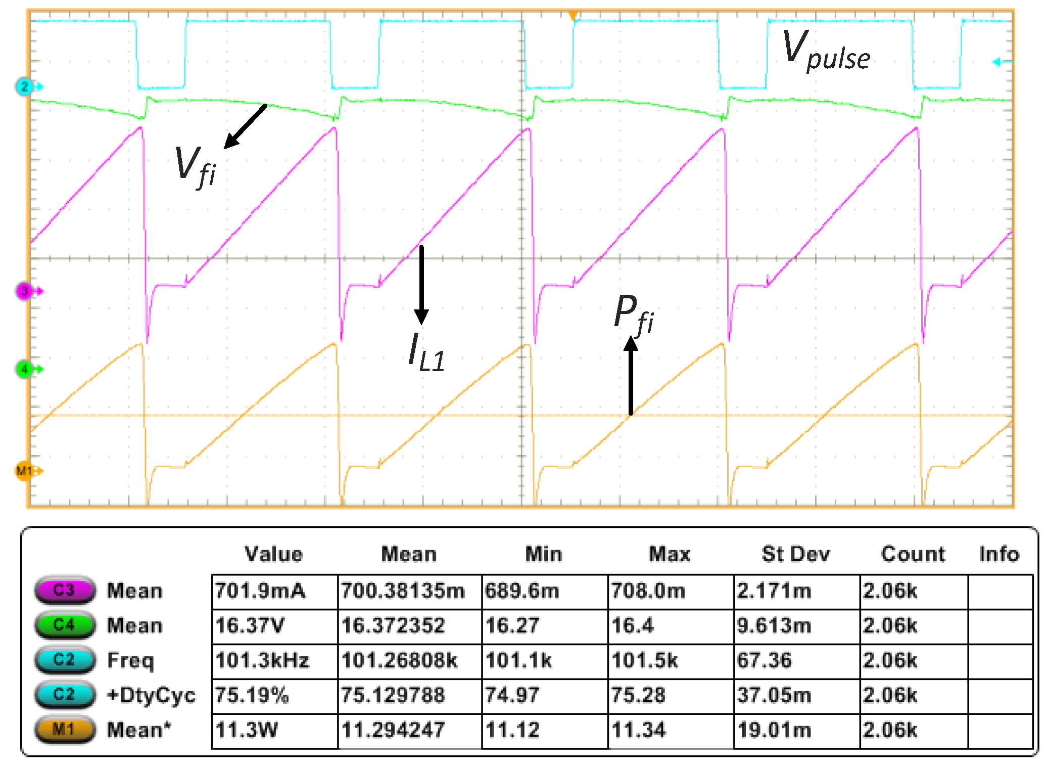
| Pfi | Flyback input power | 10.512 W |
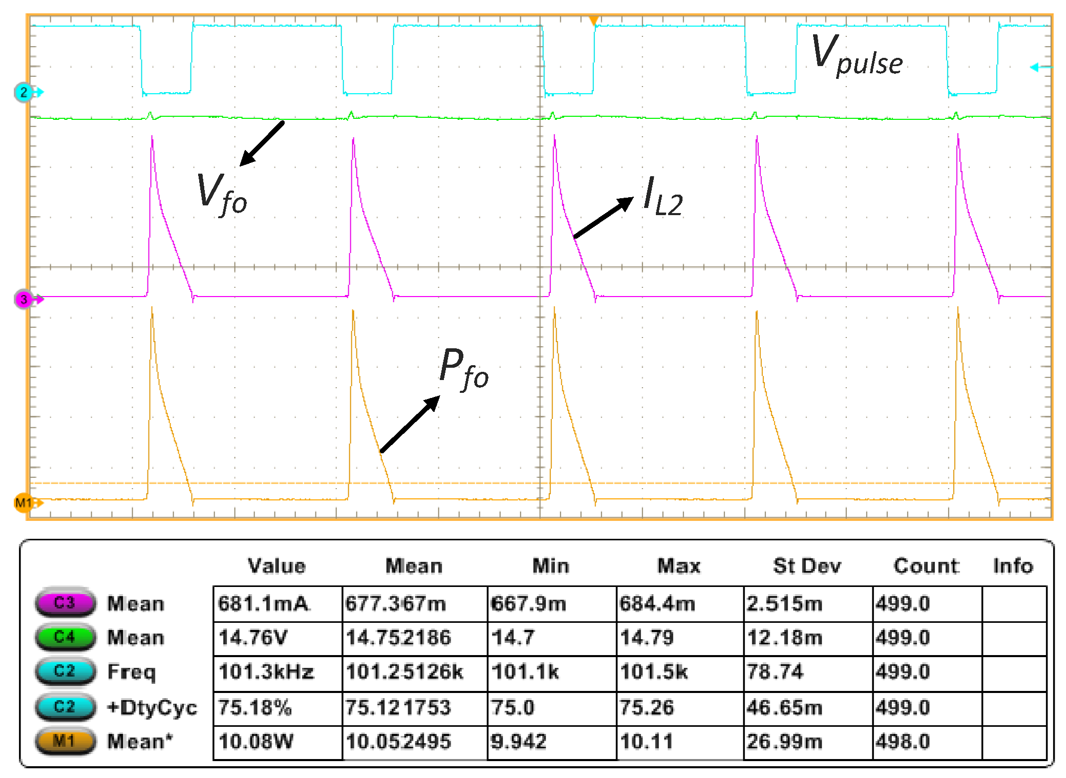
| Pfo | Flyback output power | 9.461 W |
| Q | Processed power in flyback | 51.67% |
| Mf | Flyback converter gain | 0.9625 |
| M | Converter gain | 1.4319 |
| Po-Pfo | Power delivered directly to the load | 9.93 W |
| Symbol | Quantity | Value |
|---|---|---|
| Rs | Total internal resistance of TEGs | 4.4 Ω |
| L1 | Primary inductor | 72.995 µH |
| L2 | Secondary inductor | 5.932 µH |
| Core | B66311 | |
| Coil former | EF20 | |
| Number of threads in L1 | 10 | |
| Number of threads in L2 | 12 | |
| n | Transformation relation | 3.5 |
| Np | Number of turns of primary | 32 |
| Ns | Number of turns of secondary | 9 |
| Wire gauge | 33 awg | |
| C1 | Input capacitor | 10 µF |
| C2 | Output capacitor | 10 µF |
| Ro | Load resistance | 51.8 Ω |
| M1 | MOSFET | IRF540 N |
| D1 | Diode | U1520 |
| Rsnubber | Snubber resistance | 55 Ω |
| Dsnubber | Snubber Diode | U1520 |
| Csnubber | Snubber capacitor | 5 nF |
| Parameter | Ideal | PSpice | Prototype |
|---|---|---|---|
| Input Voltage Vin | 21.3 V | 21.3 V | 21.3 V |
| Internal resistance Rs | 4.4 Ω | 4.4 Ω | 4.4 Ω |
| Input current Iin | 1.309 A | 1.3754 A | 1.272 A |
| Input power Pin | 27.88 W | 29.296 W | 27.09 W |
| Power consumed in Rs | 7.537 W | 8.4514 W | 7.036 W |
| Primary inductor L1 | 64.62 µH | 64.62 µH | 72.995 µH |
| Secondary inductor L2 | 6.65 µH | 6.65 µH | 5.932 µH |
| Flyback input power Pfi | 10.512 W | 11.945 W | 11.3 W |
| Flyback output power Pfo | 9.461 W | 10.733 W | 10.08 W |
| Load Ro | 48.22 Ω | 48.22 Ω | 51.8 Ω |
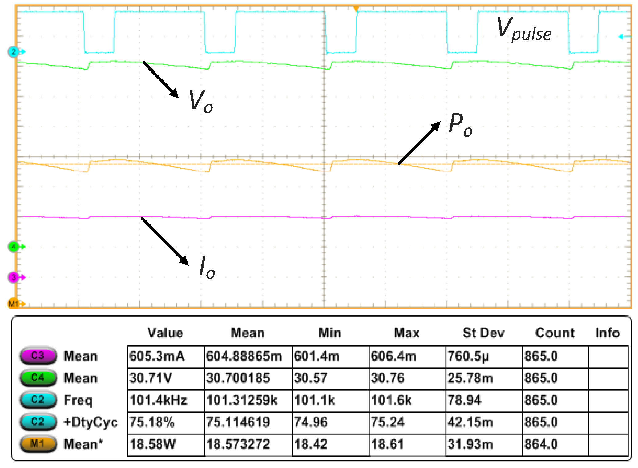
| Output voltage Vo | 30.5 V | 30.514 V | 30.71 V |
| Output current Io | 0.6325 A | 0.6328 A | 0.6053 A |
| Output power Po | 19.29 W | 19.31 W | 18.58 W |
| Processed power in flyback Q | 51.67% | 57.3% | 56.34% |
| Flyback efficiency ɳf | 90% | 89.85% | 89.2% |
| Real system efficiency ɳs | 94.82% | 92.638% | 92.65% |
| Parameter | Ideal-PSpice | PSpice-Prototype | Ideal-Prototype |
|---|---|---|---|
| Input Voltage Vin | 0.0% | 0.0% | 0.0% |
| Internal resistance Rs | 0.0% | 0.0% | 0.0% |
| Input current Iin | 5.1% | 7.5% | 2.8% |
| Input power Pin | 5.1% | 7.5% | 2.8% |
| Power consumed in Rs | 12.1% | 16.7% | 6.6% |
| Primary inductor L1 | 0.0% | 13.0% | 13.0% |
| Secondary inductor L2 | 0.0% | 10.8% | 10.8% |
| Flyback input power Pfi | 13.6% | 5.4% | 7.5% |
| Flyback output power Pfo | 13.4% | 6.1% | 6.5% |
| Load Ro | 0.0% | 7.4% | 7.4% |
| Output voltage Vo | 0.0% | 0.6% | 0.7% |
| Output current Io | 0.0% | 4.3% | 4.3% |
| Output power Po | 0.1% | 3.8% | 3.7% |
| Processed power in flyback Q | 10.9% | 1.7% | 9.0% |
| Flyback efficiency ɳf | 0.2% | 0.7% | 0.9% |
| Real system efficiency ɳs | 2.3% | 0.0% | 2.3% |
Publisher’s Note: MDPI stays neutral with regard to jurisdictional claims in published maps and institutional affiliations. |
© 2021 by the authors. Licensee MDPI, Basel, Switzerland. This article is an open access article distributed under the terms and conditions of the Creative Commons Attribution (CC BY) license (http://creativecommons.org/licenses/by/4.0/).
Share and Cite
Marroquín-Arreola, R.; Salazar-Pérez, D.; Ponce-Silva, M.; Hernández-De León, H.; Aquí-Tapia, J.A.; Lezama, J.; Saavedra-Benítez, Y.I.; Escobar-Gómez, E.N.; Lozoya-Ponce, R.E.; Mota-Grajales, R. Analysis of a DC-DC Flyback Converter Variant for Thermoelectric Generators with Partial Energy Processing. Electronics 2021, 10, 619. https://doi.org/10.3390/electronics10050619
Marroquín-Arreola R, Salazar-Pérez D, Ponce-Silva M, Hernández-De León H, Aquí-Tapia JA, Lezama J, Saavedra-Benítez YI, Escobar-Gómez EN, Lozoya-Ponce RE, Mota-Grajales R. Analysis of a DC-DC Flyback Converter Variant for Thermoelectric Generators with Partial Energy Processing. Electronics. 2021; 10(5):619. https://doi.org/10.3390/electronics10050619
Chicago/Turabian StyleMarroquín-Arreola, Ricardo, Daniel Salazar-Pérez, Mario Ponce-Silva, Héctor Hernández-De León, Juan A. Aquí-Tapia, Jinmi Lezama, Yesica I. Saavedra-Benítez, Elías N. Escobar-Gómez, Ricardo E. Lozoya-Ponce, and Rafael Mota-Grajales. 2021. "Analysis of a DC-DC Flyback Converter Variant for Thermoelectric Generators with Partial Energy Processing" Electronics 10, no. 5: 619. https://doi.org/10.3390/electronics10050619
APA StyleMarroquín-Arreola, R., Salazar-Pérez, D., Ponce-Silva, M., Hernández-De León, H., Aquí-Tapia, J. A., Lezama, J., Saavedra-Benítez, Y. I., Escobar-Gómez, E. N., Lozoya-Ponce, R. E., & Mota-Grajales, R. (2021). Analysis of a DC-DC Flyback Converter Variant for Thermoelectric Generators with Partial Energy Processing. Electronics, 10(5), 619. https://doi.org/10.3390/electronics10050619