Article

Variable Clock and EM Signal Generation Scheme for Foveation-Based Driving OLED Head-Mounted Displays

Department of Information Display, Kyung Hee University, Seoul 02447, Korea
*
Author to whom correspondence should be addressed.
These authors contributed equally to this work.
Electronics 2021, 10(5), 538; https://doi.org/10.3390/electronics10050538
Submission received: 28 January 2021 / Revised: 17 February 2021 / Accepted: 20 February 2021 / Published: 25 February 2021
(This article belongs to the Section Circuit and Signal Processing)

Abstract

:
An image processing pipeline and multi-output shift register of a foveation-based driving scheme are proposed for the realization of immersive head-mounted displays in 2019. In addition, this paper describes a variable clock generation circuit to manipulate output waveforms of shift registers in the foveated display. The EM circuit for OLED displays is also introduced to support the control signal to keep OLEDs of pixels from emitting light during the compensation. Especially, the EM circuit consists of only four TFTs and one capacitor and gives rise to pulses of variable widths corresponding to the resolution of a driven display area. A variable clock generation scheme is verified with 60 Hz 1440 × 2560 monitor, eye-tracker, PSoC board and FPGA board. An EM circuit is simulated by SPICE for 9600 lines and 120 Hz foveated displays.

1. Introduction

Due to the recent global pandemic of coronavirus 2019 (COVID-19), societies are being changed from offline to online. Virtual reality (VR) is one of the key technologies to support these online activities in a variety of fields including education, conference, manufacturing and researching [1,2,3,4,5].
The realization of these VR technologies requires high resolution, wide field-of-view (FoV) and high frame rate displays that make indistinguishable visual experiences possible [6,7,8,9,10]. These high-performance displays can ameliorate screendoor effects, motion artifacts and latency, providing users with immersive experiences. However, it is too difficult to meet these three requirements at the same time. While many studies have focused on the latency reduction by means of the foveated rendering at the graphics processing unit [11], the data bandwidth reduction [12] and the deep learning for motion tracking [13], until recently, there remained one critical problem on the display side. which is the insufficient pixel charging time because of the very high resolution of several thousand lines and the frame rate faster than 60 Hz. Ideally, the visual acuity of 60 pixels per degree (ppd) and horizontal and vertical FoVs of 160 ° and 170 ° for each eye should be satisfied with high resolution displays of around 9600 lines. At this resolution, only a charging time smaller than 0.87 μs, which is too short to charge pixel electrodes fully, is allowed at a 120 Hz frame rate.
On the other hand, this insufficient charging time can be coped with by the foveation-based driving scheme that extends the line time by means of multiple line driving gate driver and foveated rendering in the panel [14]. The multiple lines of the high resolution input image are compressed in a line by different factors according to the distance from the foveation point and the human visual system (HVS). Then, pixels of these multiple lines are charged with the same voltage leading to the reduction on the effective number of lines by 79.0% for the resolution of 9600 lines. As a consequence, the charging time is extended from 0.87 to 4.14 μs.
The previous proposal [14] showed the overall architecture and multi-output shift registers; however, the variable clock generation block is needed to drive those shift registers because variable gate pulses are produced by clock signals. Furthermore, to apply this foveation-based method to organic light-emitting diode (OLED) displays, emission (EM) signals should be applied to the pixel circuits to keep OLEDs from emitting light when the compensation is being conducted over threshold voltage, mobility and supply voltage variations [15,16,17,18,19,20].
This paper proposes variable clock generation scheme for multi-output shift registers and EM signal circuit for the OLED pixel compensation. Consequently, the foveation-based OLED display is fully accomplished with small area multi-output shift register, simple variable clock generation, EM circuit of only four thin film transistors (TFTs) and vertical resolution reduction just by averaging. This leads to the high resolution and high frame rate display by means of line time extension as well as the reduction of data bandwidth and latency.

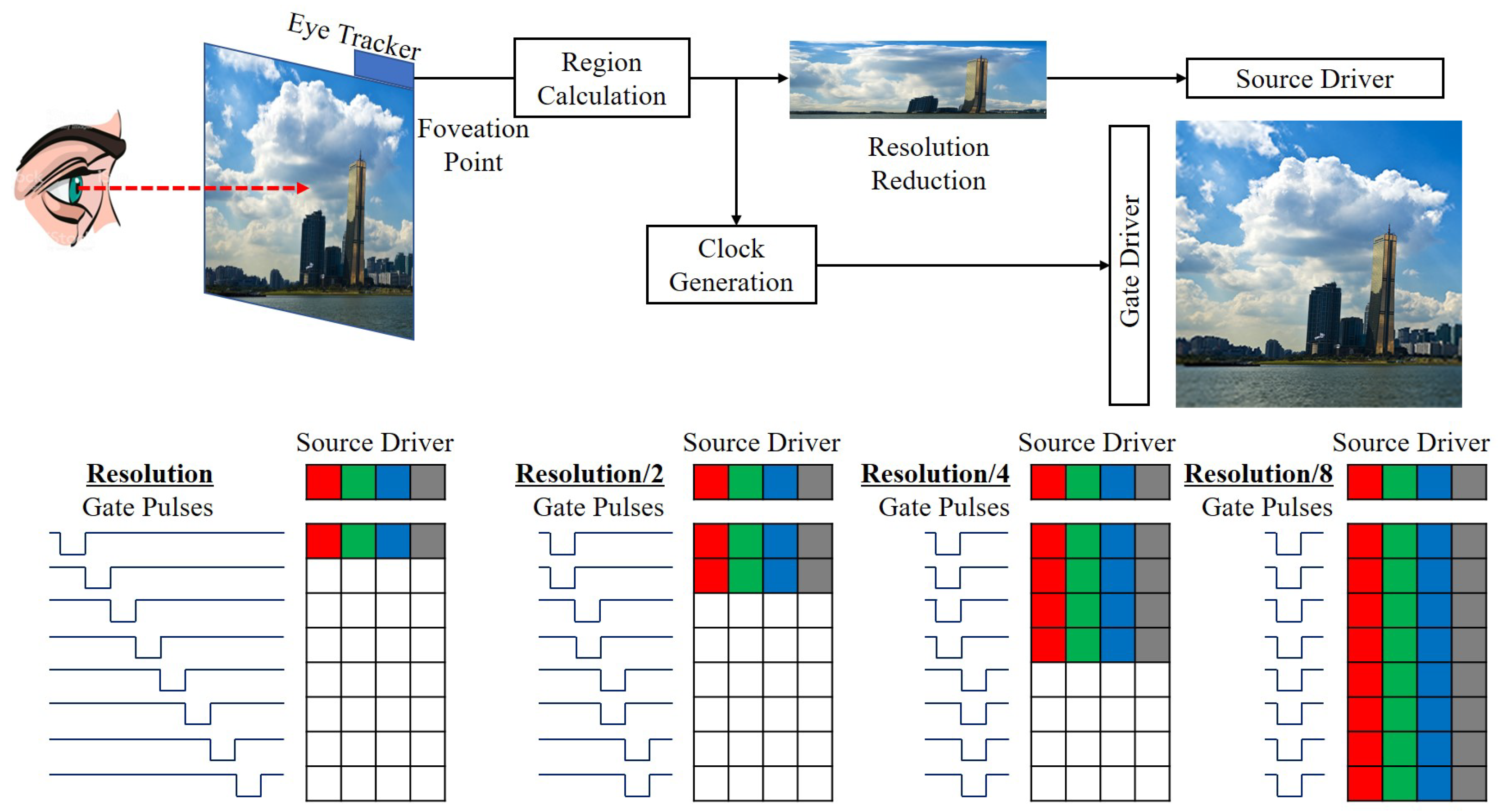
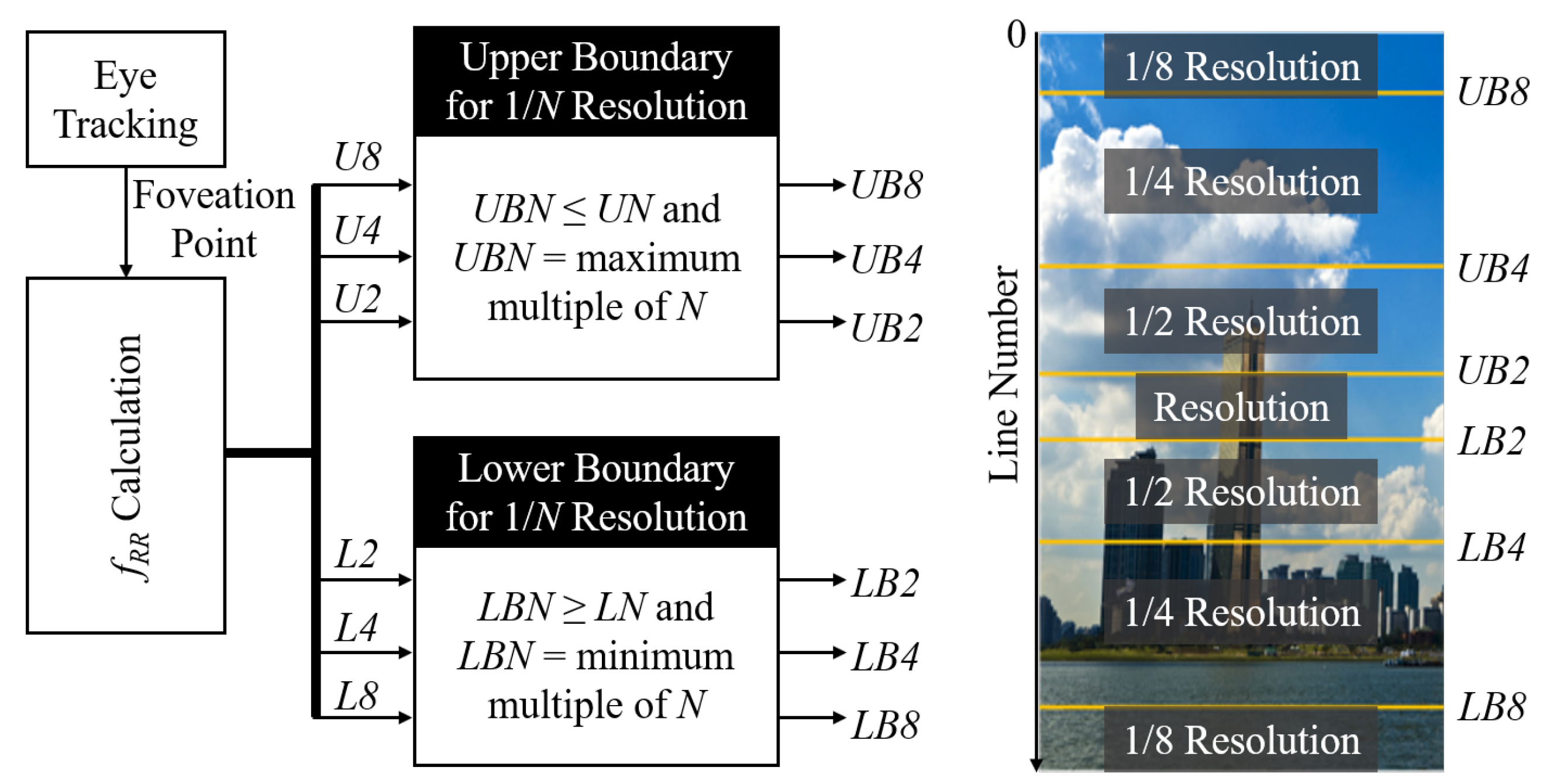
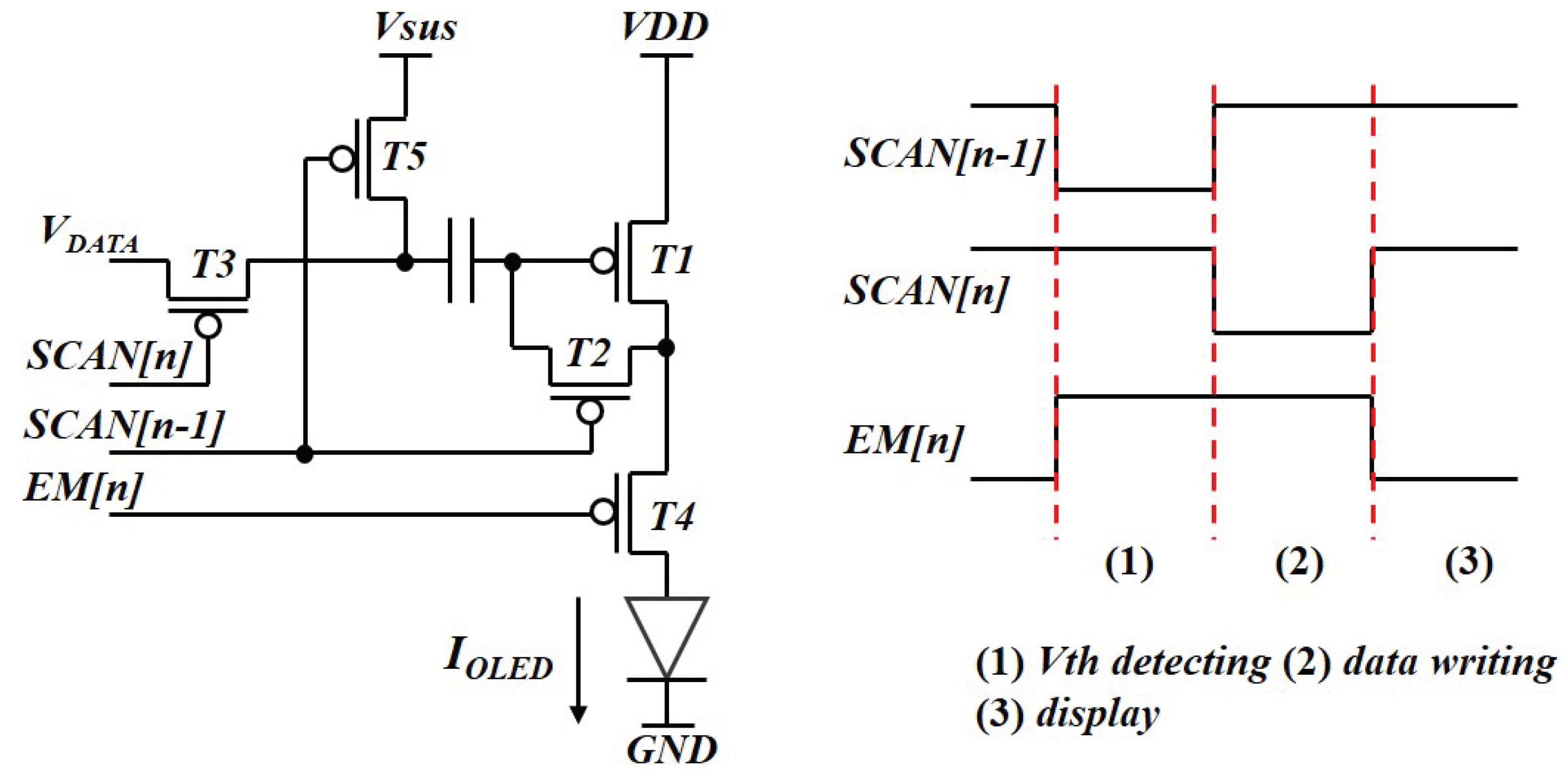
2. Previous Foveation-Based Driving Scheme

The perceivable spatial frequency of a displayed image is limited by the non-uniform distribution of receptor cells in the retina of HVS and the finite resolution of a display. Consequently, the maximum perceivable frequency ( f H V S ) of HVS is expressed by Equation (1) and the display resolution defined as a half Nyquist frequency ( f R E S ) by Equation (2) for the eccentricity (e) that is the distance from the foveation point in the unit of degree. V is the vertical resolution of the display, β V is the viewing distance between eye and head mounted display (HMD), e 2 is a half-resolution eccentricity constant, C T 0 is a minimal contrast threshold and α is a spatial frequency decay constant [21]. The resultant cutoff frequency ( f c ) is obtained as the minimum value among f H V S and f R E S , as expressed in Equation (3).
f H V S ( e ) = e 2 ln C T 0 α ( e 2 + e ) [ c y c l e s / d e g r e e ]
f R E S ( e ) = π β V 360 · cos 2 π e 180 [ c y c l e s / d e g r e e ]
f c = min f H V S , f R E S
When a flat panel display is used as a HMD, f R E S is increasing and f H V S is decreasing over the distance from the foveation point ( d p i x e l ). While f c is equal to f R E S in only some region around the foveation point, f c is determined by f H V S in the outside area. If the resolution is reduced by 2 n (n = 1, 2,… ), the larger region of f c is controlled by the display resolution because a corresponding Nyquist frequency ( f R E S / 2 n ) moves to the lower values. However, there still exists the area dominated by f H V S in the reduced resolutions. Therefore, resolutions of display areas ( f R R ) can be further reduced while the resultant f c is perceptually equivalent to that of the original resolution image without any visible artifacts [14].
The previous foveation-based driving scheme is composed of vertical resolution reduction and multi-output driving gate circuit [22,23], as depicted in Figure 1, where the low-level gate pulses enable the pixel charging by assuming that the display panel is manufactured at a backplane of p-channel TFTs. The vertical resolution reduction curtails the vertical resolution of the input image with the much smaller number of lines by merging multiple-line pixels into one-line pixels with their average values in accordance with f R R . Then, these merged pixel data are driven to pixels of corresponding multiple lines in a panel at a time by the multi-line driving circuit. In the end, the full resolution foveated image is given rise to directly in a panel from the reduced resolution image, which allows the pixel charging time to be extended. While the previous study proposed the overall architecture and the multi-output shift register, this paper introduces the clock generation scheme to support the variable clock waveforms for the multi-output shift register as well as the variable pulse width EM circuit for the pixel compensation in OLED displays.

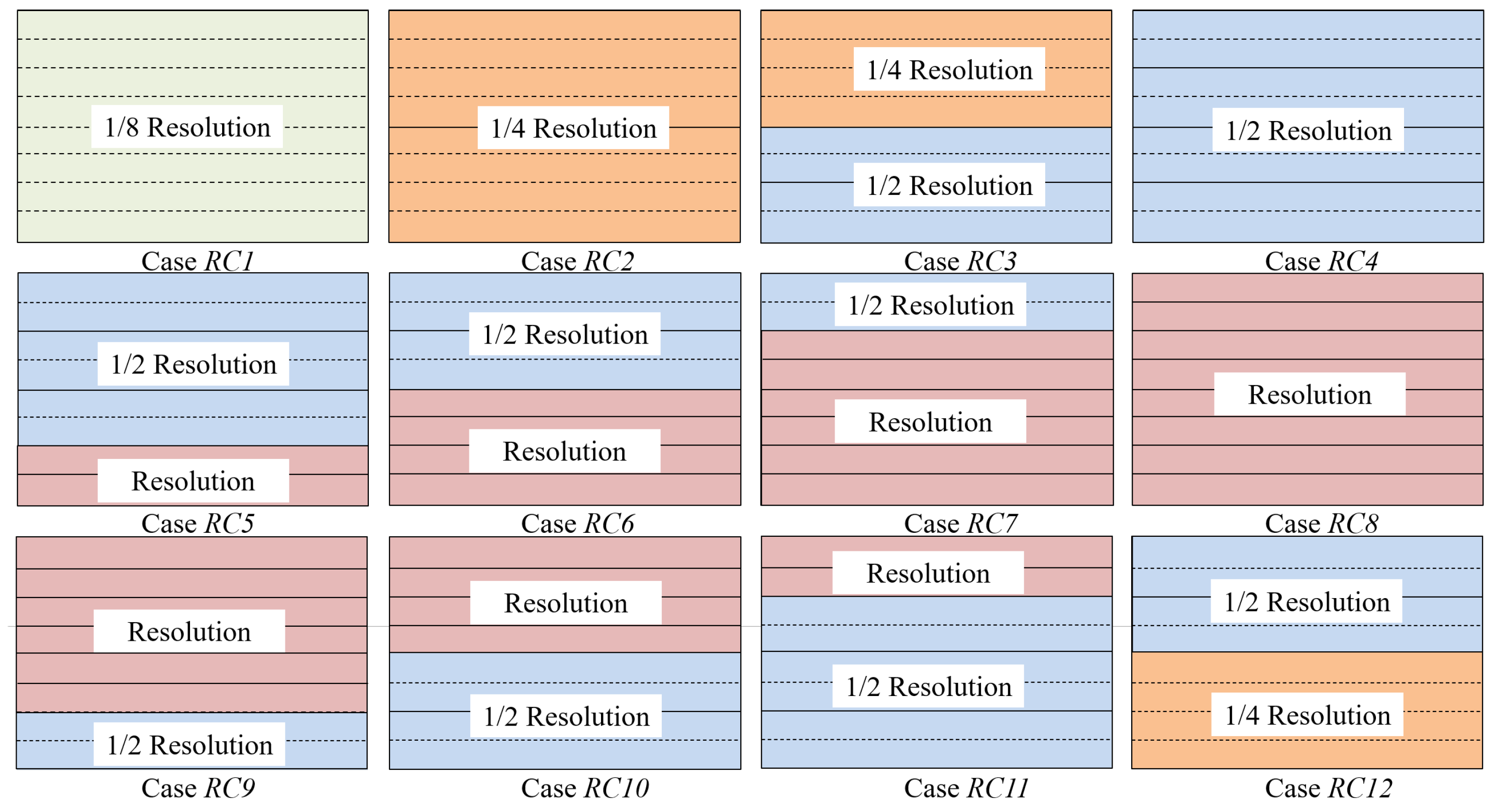
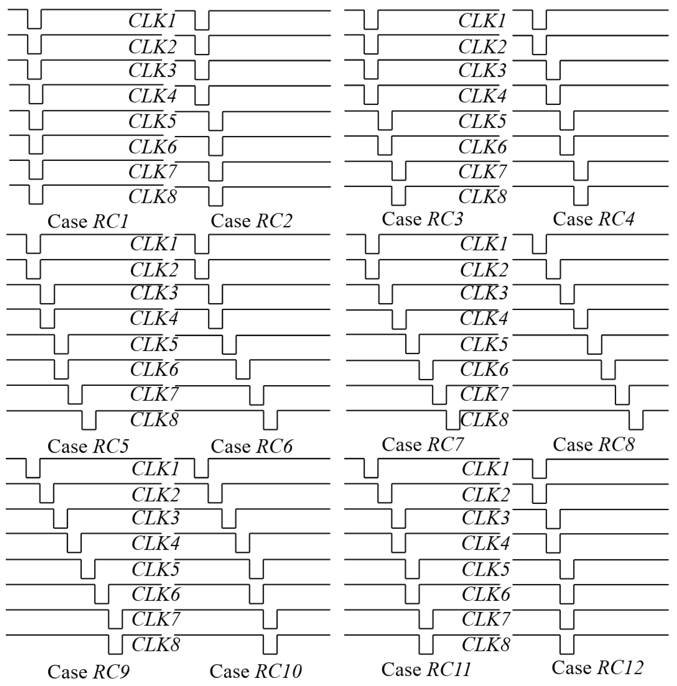
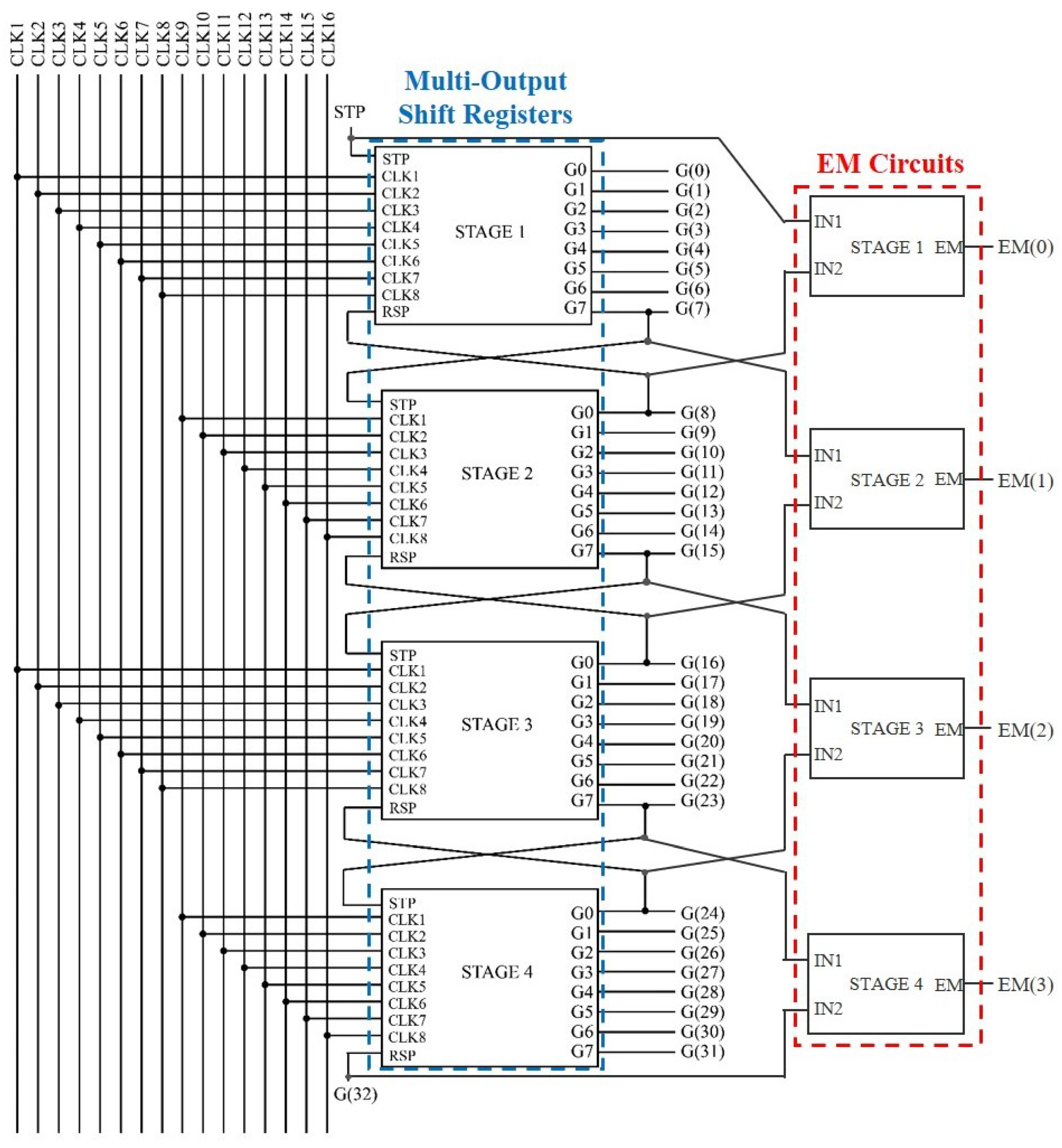
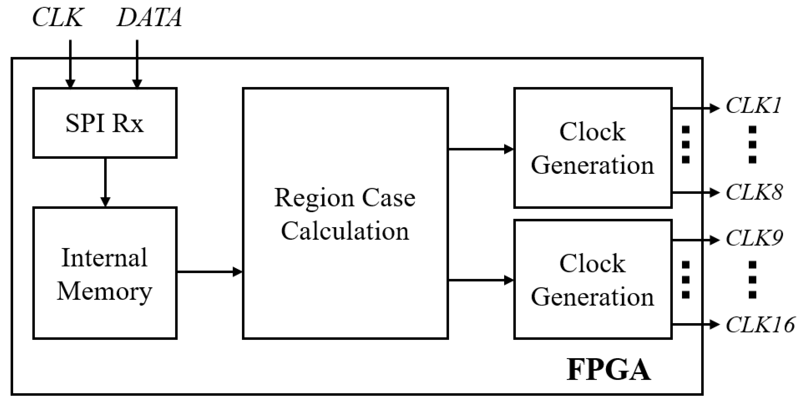
3. Variable Clock Generation

The previous foveated display [14] employed eight-output shift registers in gate driver circuits. While a variety of pulse timings are programmable within the outputs of one shift register, there should exist one-clock shifts between adjacent shift registers. Consequently, it has to be ensured that output pulses of the same timing are generated only in a single shift register. Using the foveation point obtained by an eye tracking module and f R R , upper and lower region boundaries of 1/2, 1/4 and 1/8 resolutions are calculated accordingly, where U2, U4 and U8 are the boundary line numbers for upper regions and L2, L4 and L8 for lower regions. Then, the boundaries of regions are adjusted to be multiples of tw, four and eight, which guarantees that multiple pulses with the equal timing are given rise to in a shift register. For the upper regions, the adjusted values (UB2, UB4 and UB8) are determined to be maximum multiples that are equal to or smaller than U2, U4 and U8. Conversely, the values of the lower regions (LB2, LB4 and LB8) are adjusted to be minimum multiples that are equal to or larger than L2, L4 and L8. As a result, no resolution regions are overlapped over two shift registers. This boundary adjustment is summarized in Figure 2.
After the boundaries are computed, clock pulses are controlled to generate gate pulse waveforms corresponding to regions. Since output pulses of multi-output shift registers are equivalent to clock pulses during their output periods, it is required to change clock waveforms according to the resolution of the panel region driven by gate pulses. In the region of a shift register, there are 12 possible cases, as shown in Figure 3, which can be determined from boundary values. For example, when the foveation point is placed on the center of a display, the top region can be assigned with 1/8 resolution. As the region gets closer to the foveation point, the resolutions increase up to the original resolution through the case RC1 to the case RC8. After passing the center, the resolutions decrease down to 1/8 resolution at the bottom area through the case RC9 to the case RC11, the case RC4, the case RC12 and the cases RC2 and RC1 again. The cases RC3, RC5, RC6, RC7, RC9, RC10, RC11 and RC12 represent that the boundaries are located at the inside of the region controlled by one shift register. After one region case is determined, a corresponding clock waveform is selected among 12 cases, as illustrated in Figure 4, and are transferred to shift registers. In a 1/8 resolution region, all eight clock signals give rise to pulses at the same time. In the same way, in 1/4 and 1/2 resolution regions, four and two clock signals provide pulses at the same time. Then, for the original resolution region, clock signals should be shifted over their previous ones by one pulse width.
On the other hand, as the foveation point moves, the effective number of lines in the reduced resolution image also changes. It has the maximum value for the foveation point in the center of a panel, while it gets to be the minimum for the foveation point in the uppermost and lowermost positions of a panel. To support fixed frame and line times even at this variable effective number of lines, the variation on the vertical blank length, which is recently used to support the variable frame rate in gaming and low power display applications [24,25], maintains the total number of vertical lines including vertical active and blank areas at the constant number. For example, when the effect numbers of lines at the center and uppermost positions are 1456 and 928 for the vertical resolution of 4800 lines [14], the vertical blank lengths are set to be 14 and 542, respectively. Consequently, this vertical blank adjustment leads to the constant total number of vertical lines of 1470 for any foveation points. Unlike the variable frame rate applications, this vertical blank variation scheme causes no flicker problems because the frame rate is maintained at the fixed value [22,26].

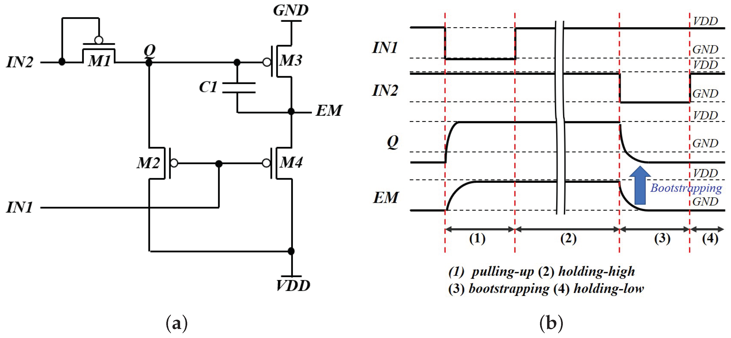
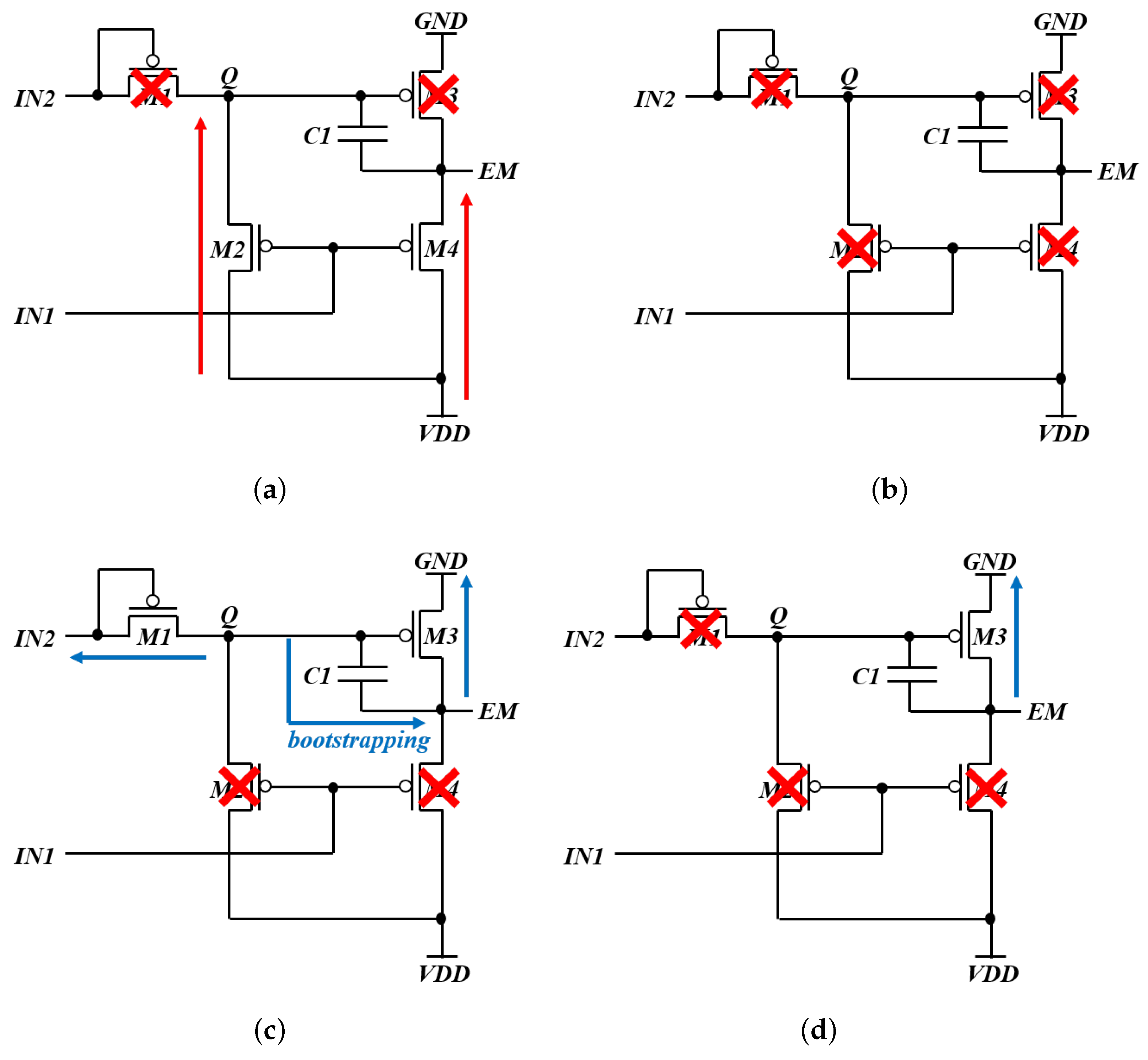
4. EM Signal Generation for OLED Pixels

As mentioned above, high quality OLED displays need to compensate for variations on TFTs’ electrical characteristics over area and time as well as supply voltage drops. The example pixel circuit shown in Figure 5 [27] is able to compensate for both threshold voltage ( V t h ) of T1 and voltage drop of VDD. In the V t h detecting period, the capacitor stores the voltage of V D D | V t h | V s u s and the following data writing period programs the gate voltage of T1 at V D D | V t h | V s u s + V D A T A leading to the OLED current ( I O L E D ) independent of VDD and V t h at the display period, as described in Equation (4), where k is a coefficient.
I O L E D = k 2 ( V s u s V D A T A ) 2
The control signal of EM connected to a p-channel TFT (T4) is applied at the high voltage level to make the drain of T1 floating and to keep the OLED from emitting the undesired light during both V t h detecting and data writing periods. These EM pulses, which are wider than gate pulses, have been generated by additional shift registers with wide clock pulses or programmable pulse width shift registers [28,29,30]. While previous circuits maintain the pulse width of EM signals to be equivalent for all pixels, EM pulse widths for these foveation-based driving pixels should be adjusted differently depending on the resolution of the driven panel area. The proposed scheme assigns one EM signal to eight lines driven by one multi-output shift register. That is, all pixels in these eight lines are turned off during the same period of time that is different according to the resolution of the assigned region.
Assuming that the panel is implemented at the backplane of p-channel TFTs and the high level of the EM pulse turns off the light emission, the proposed EM pulse circuit is simply composed of only four TFTs, as presented in Figure 6a. Whereas the IN1 pulse pulls up the voltage of Q and EM, the IN2 pulse pulls down Q as well as EM. As depicted in Figure 6b, EM is charged during the interval between IN1 and IN2 pulses and is maintained at the low level for the remaining period of time. Because of the Q node voltage bootstrapped through C1, EM can be driven at GND without any voltage rises. Since Q turns into a floating node at GND more quickly than EM due to the smaller capacitive load, the voltage difference between Q and EM is stored across C1, and this difference is maintained during the falling transition of EM. Therefore, Q is bootstrapped to lower than GND. The last output of the previous shift register is applied to IN1, and the first output of the following shift register is asserted to IN2, as illustrated in Figure 7 where CLK1CLK8 are connected to odd shift registers and CLK9CLK16 are used for even shift registers. When the example pixel circuit in Figure 5 is used, the V t h detecting operation takes place at the same time as the last pulse of the previous shift register in all pixels of eight lines and data writing operations work for pixels of corresponding lines to pulses of the current shift register. Then, the first pulse of the next shift register triggers the light emission of those pixels.
The detail operations are explained with four periods of pulling-up, holding-high, bootstrapping and holding-low. In the pulling-up period in Figure 8a, because M1 and M3 are turned off, Q and EM are pulled up to VDD through M2 and M4. Then, in the holding-high period in Figure 8b, Q and EM are retained at VDD as all TFTs from M1 to M4 are turned off. In the bootstrapping period in Figure 8c, M1 and M3 are turned on; however, Q is pulled down more quickly than EM owing to its smaller capacitive load. Therefore, Q becomes a floating node that allows the falling transition of EM to boost the voltage of Q to the lower level than GND by the bootstrapping through C1. Consequently, EM can be pulled down to GND. In the end, in a holding-low period of Figure 8d, Q is kept at the low voltage level to turn M3 on by C1, even though there exist leakage currents at M1 and M2. EM is also held at GND during a frame time. Although this EM circuit is based on the basic structure of a shift register, the connection of M3 to a constant supply GND instead of clocks avoids the fluctuation on Q and EM nodes without additional TFTs [31].

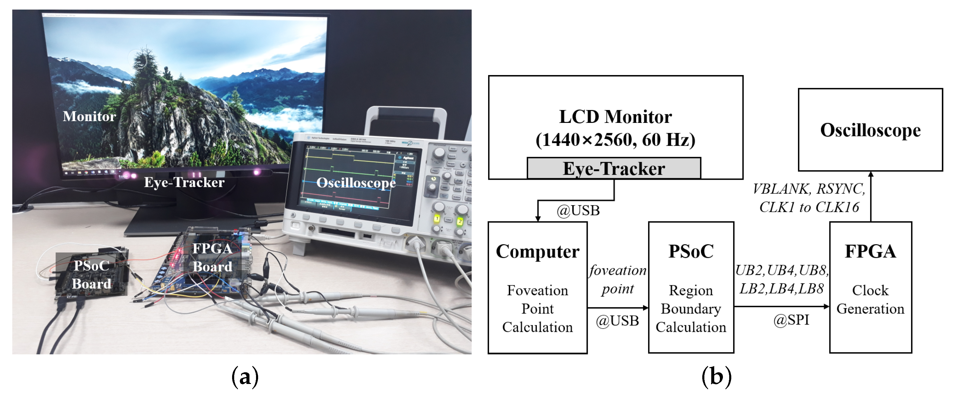
5. Evaluation Results

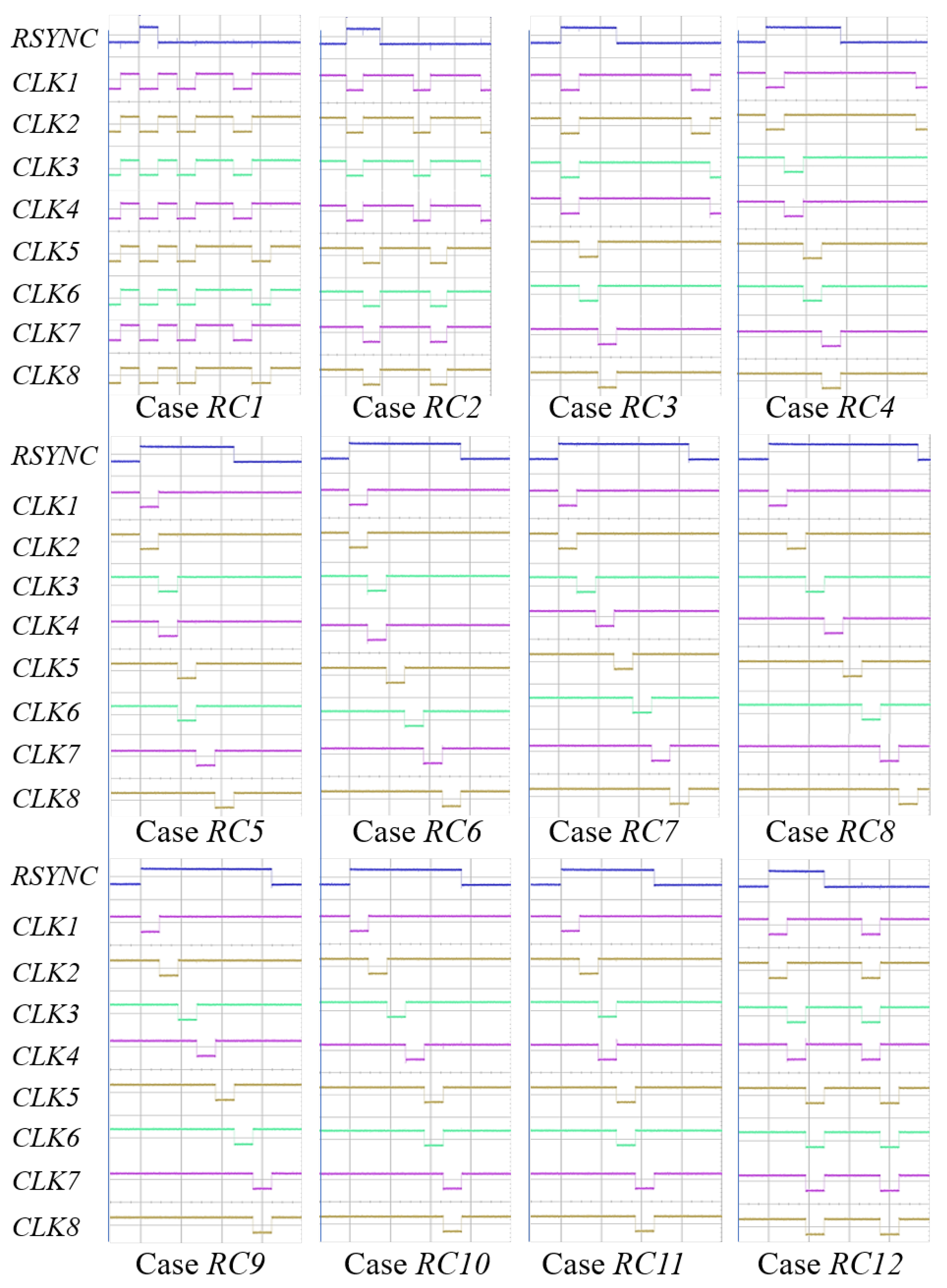
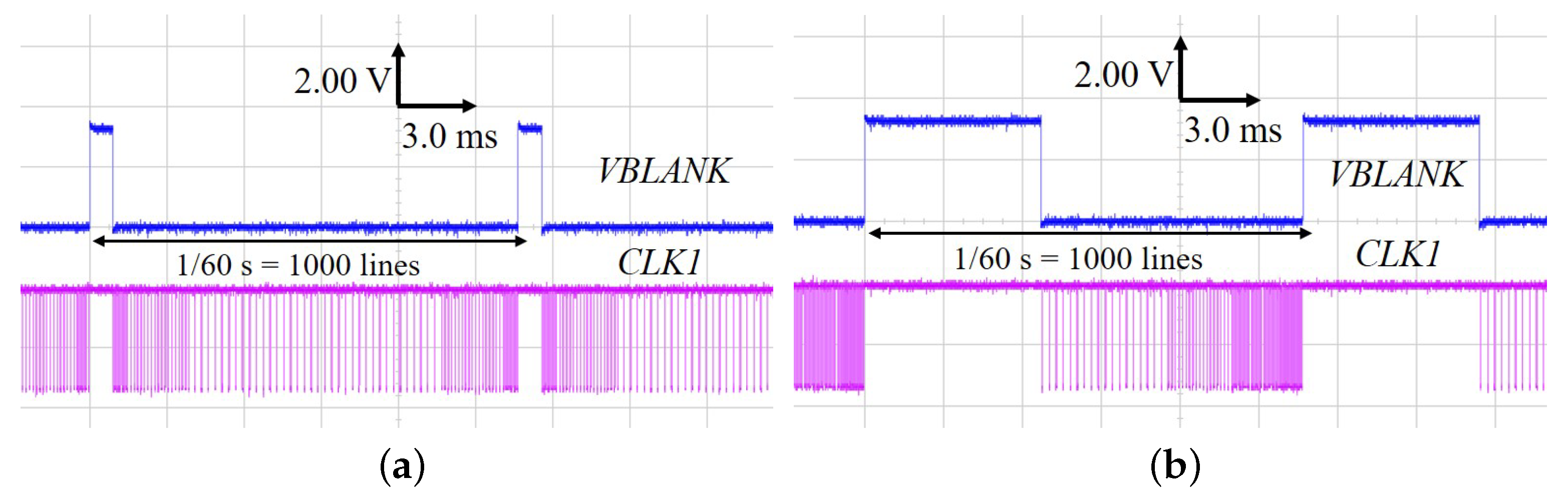
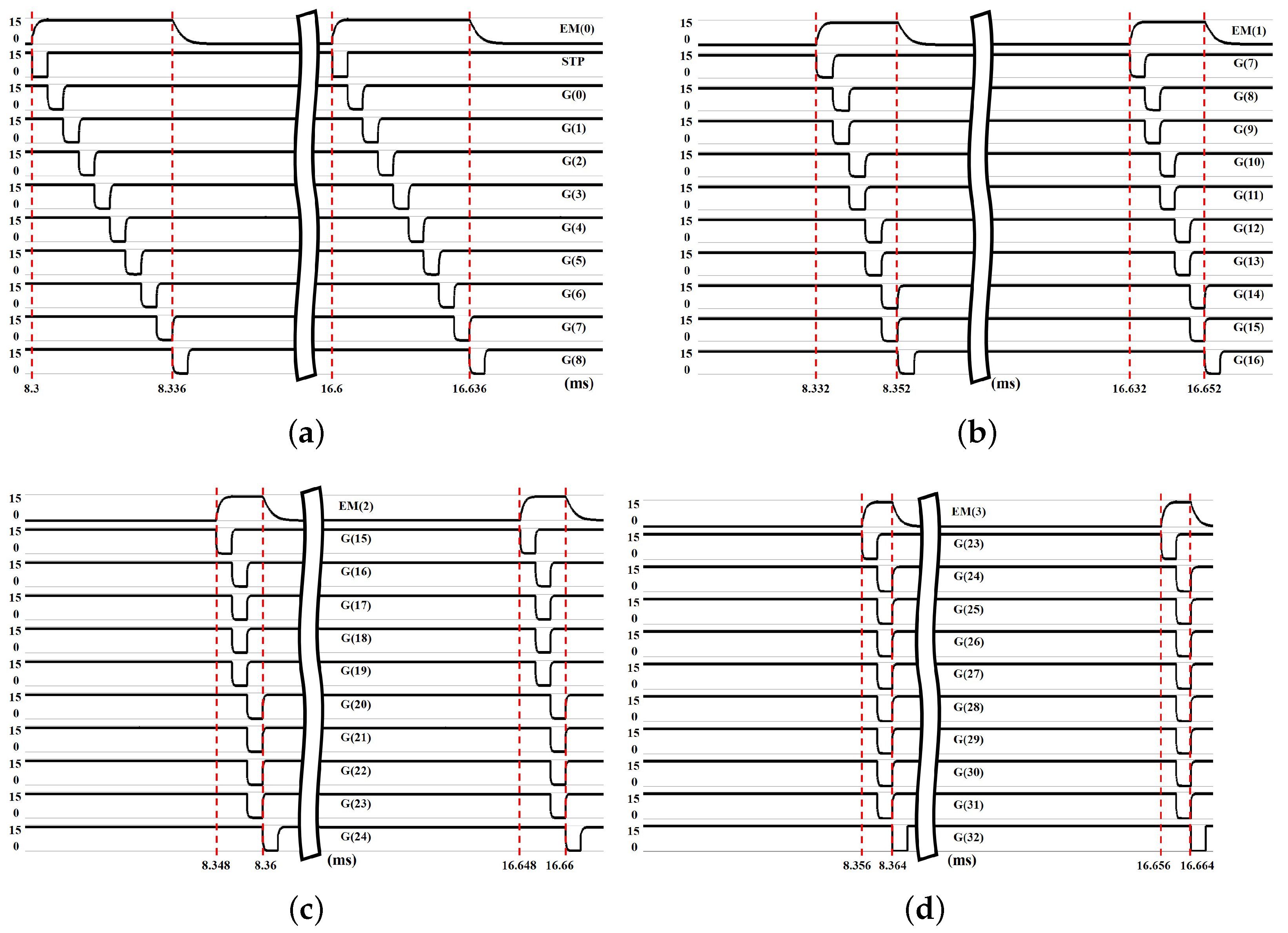
5.1. Variable Clock Generation

The variable clock generation circuit was evaluated using 60 Hz 1440 × 2560 liquid crystal display (LCD) monitor, eye-tracker (Tobii Eye Tracker 4L) [32], computer, programmable system on chip (PSoC) board (Cypress PSoC 5LP) [33] and field programmable gate array (FPGA) board (Terasic DE2-115) [34], as shown in Figure 9a. The eye-tracker is attached at the bottom of a monitor to capture the foveation point, which is sent to a computer via a universal serial bus (USB) interface. The computer estimates the coordinate of the foveation point and transmits it to a PSoC board with an USB interface. Because the used FPGA board cannot handle the USB interface directly, the PSoC is used to convert the USB data into serial peripheral interface (SPI) data. In addition, because the PSoC contains a central processing unit (CPU), it calculates boundary values of UB2, UB4, UB8, LB2, LB4 and LB8 and transfers them to a FPGA board through the SPI. These resolution boundaries are calculated at the viewing distance parameter, β of 0.35. Finally, the FPGA board outputs VBLANK, RSYNC and 16 clock signals of CLK1 to CLK16. VBLANK is the signal that indicates the vertical blank period, and RSYNC is used to show the specific region case in the oscilloscope. This connection is explained in more details in Figure 9b.
The FPGA board stores six received boundary values of each 14 bits in the internal block memory and loads them right before starting a new frame. These boundary values are compared with the current region driven by the multi-output shift register, and then one of 12 regions in Figure 3 is selected in the region case calculation, leading to the determination of a clock waveform out of 12 cases. Finally, two clock generation blocks give rise to eight clocks of CLK1 to CLK8 for even shift registers and eight clocks of CLK9 to CLK16 for odd ones. Eight clock signals are made by the 8-bit pattern sequence each line time for a selected region case. For example, the case RC2 is supported by the sequence of two 8-bit binary numbers that are 11110000 and 00001111 for CLK1 to CLK8. The case RC4 consists of four 8-bit binary numbers that are 11000000, 00110000, 00001100 and 00000011. The block diagram of this variable clock generation circuit is depicted in Figure 10. The measured waveforms for 12 cases are presented in Figure 11 where the first pulse, RSYNC, is generated to indicate the corresponding region case in an oscilloscope. The clock signals are successfully given rise to for their region cases, which are exactly matched to the target waveforms of Figure 4.
Additionally, the variation of the reduced vertical resolution from the maximum to the minimum is realized by changing the foveation point from the center position to the uppermost position on the monitor. Then, the clock signals are generated based on the foveation points obtained by the eye tracker. To keep the frame time at the constant value, the vertical blank length is adjusted as depicted in Figure 12. The pulse interval of CLK1 is wider at the higher resolution area because outputs of one shift register are generated for more line times. Thus, the foveation point area is recognized by finding where the sparser CLK1 pulses appear. In our evaluation setup where the frame time is fixed at 1000 lines, while lengths of active and vertical blank areas are 950 lines and 50 lines for the foveation point at the center, they are adjusted to be 602 lines and 398 lines at the uppermost. All clock pulses of the vertical blank period are deactivated.

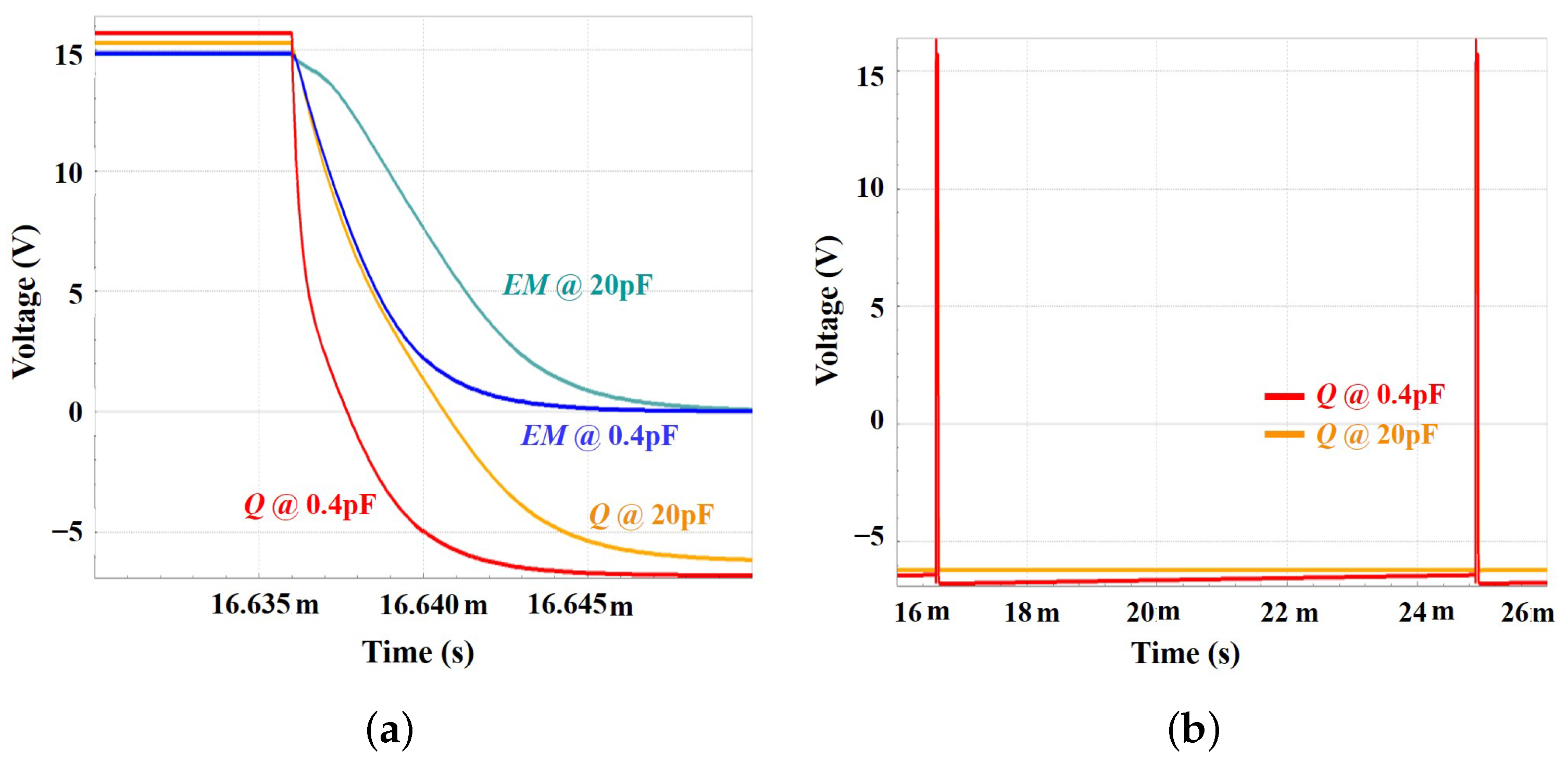
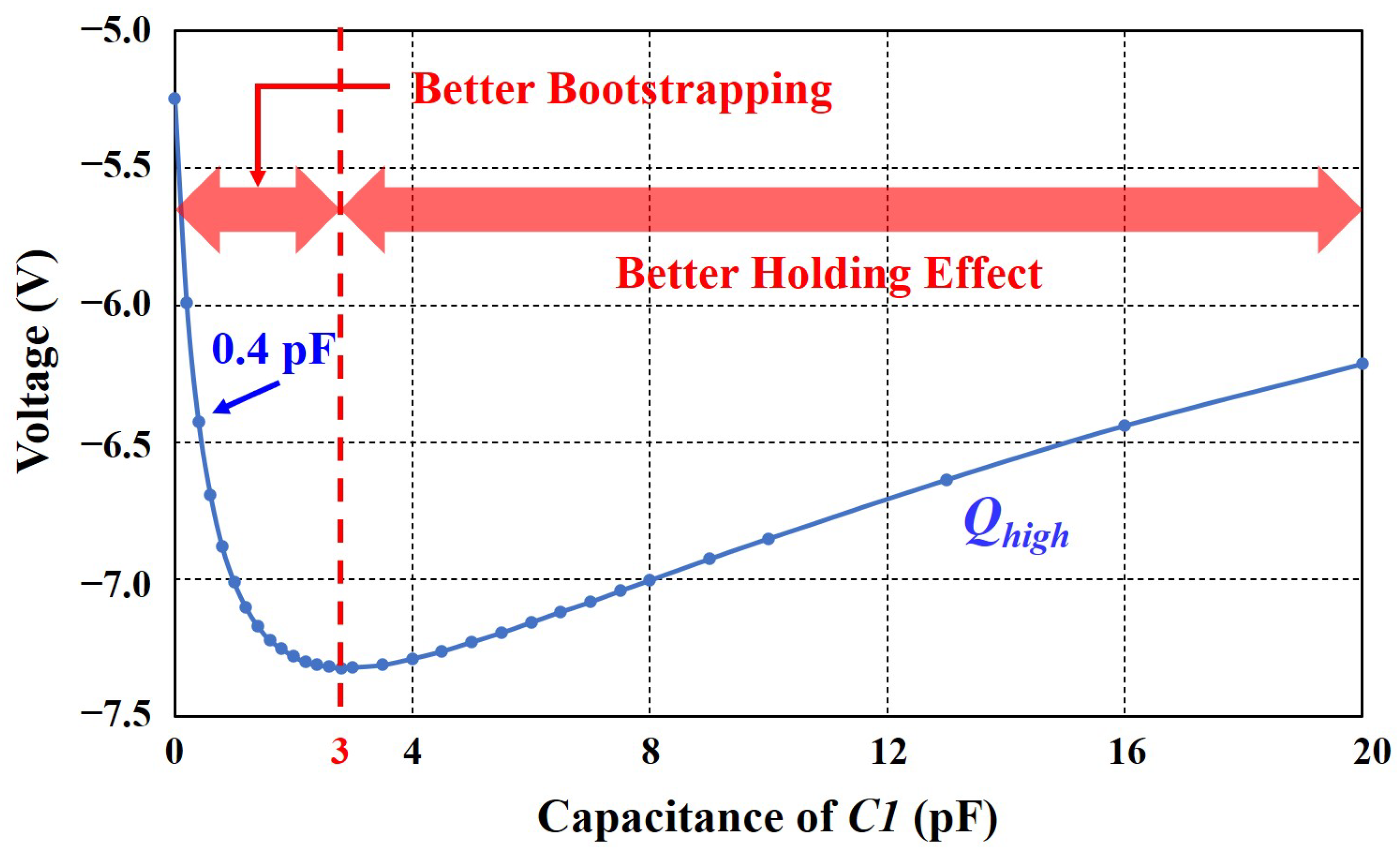
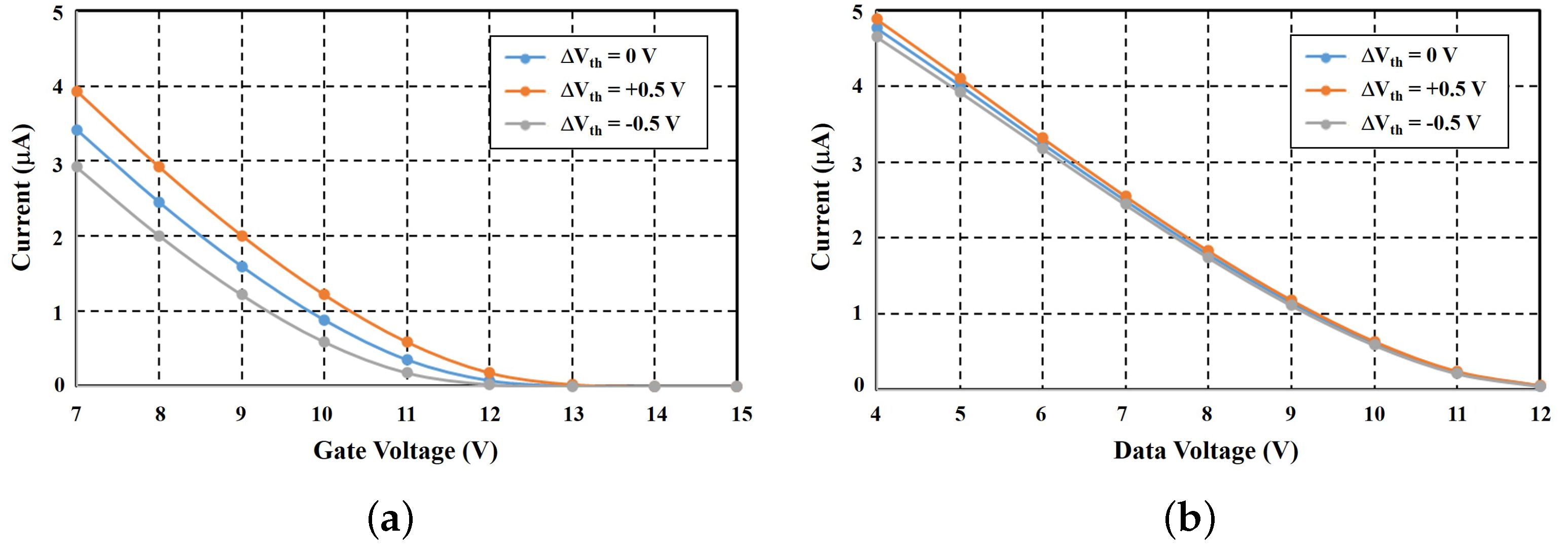
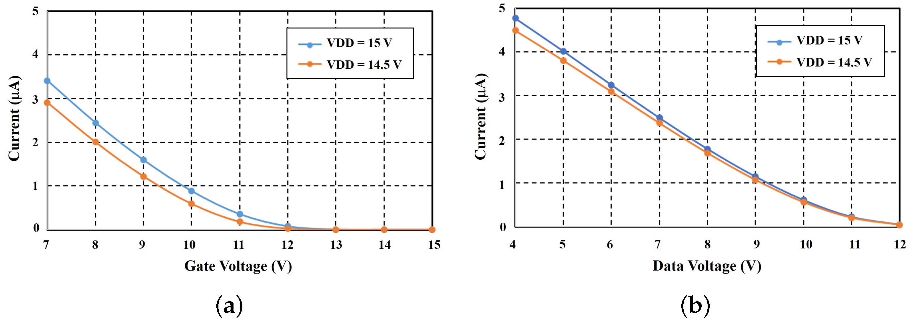
5.2. EM Signal Generation

The proposed EM circuit was simulated by SmartSpice [35] with a p-channel low temperature poly silicon (LTPS) TFT model where threshold voltage, mobility and overlap capacitance of TFTs are −1.7 V, 31 cm 2 /V·s and 3.02 fF / μ m, respectively. All channel lengths are set to be 7 μm and the channel widths of M1, M2, M3 and M4 are 10, 10, 100 and 100 μm, respectively, to drive resistive and capacitive loads of 2.2 k Ω and 120 pF [22] in a line time that is set to be 4.14 μs for a 120 Hz foveated display. The supply voltage levels of VDD and GND are 15 and 0 V. They are summarized in Table 1.
To determine C1, changes of holding effect, bootstrapping and falling time at the Q node are investigated regarding its capacitance. If C1 is given as 0.4 pF to be much smaller than the capacitive load at EM, Q reaches to a floating state of GND+| V t h | earlier than EM leading to the big voltage difference between Q and EM, as presented in Figure 13a. This achieves large bootstrapping at Q that results in the fast falling transition at EM. Conversely, because the large C1 of 20 pF slows down the falling transition of Q, it causes the small difference between Q and EM, degrading the bootstrapping of Q and the falling speed of EM. However, the larger C1 improves the holding effect leading to the reduced voltage rise caused by the leakage currents, as shown in Figure 13b. Consequently, there exists the trade-off between holding effect and bootstrapping where the larger C1 degrades the bootstrapping effect with better holding capability, but the smaller C1 increases the voltage rise at Q by the leakage current with larger bootstrapping. Since the maximum boosted Q voltage for a frame time ( Q h i g h ) is important to maintain the turning-on state of a pull-down TFT (M3), the capacitance of C1 is determined using the plot of Q h i g h , as shown in Figure 14. When C1 is less than 3 pF, the full bootstrapping effect takes place but the current leakages pull up the Q voltage level during a frame time owing to the poor holding effect. On the other hand, when C1 is larger than 3 pF, the boosted voltage level at Q goes up due to the bootstrapping degradation in spite of the improved holding performance. In addition, considering the size of the EM circuit, the final C1 has been determined as 0.4 pF with Q h i g h of −6.4 V, where the falling transition of EM is completed in a line time of around 4 μs.
The simulation was conducted for the configuration of shift registers and EM circuits in Figure 7 where the first, second, third and fourth stages are assigned to f R E S , f R E S / 2 , f R E S / 4 and f R E S / 8 regions, respectively. Their corresponding cases of clock waveforms are RC8 for f R E S , RC4 for f R E S / 2 , RC2 for f R E S / 4 and RC1 for f R E S / 8 in Figure 4. The simulated waveforms are shown in Figure 15. As a consequence, the first shift register of f R E S produces eight shifting pulses from G(0) to G(7) and the corresponding EM circuit generates the EM(0) pulse of the low level during nine line times. In the same fashion, the second shift register and EM circuit of f R E S / 2 build gate pulses from G(8) to G(15) and EM(2) of five line times, the third ones of f R E S / 4 from G(16) to G(23) and EM(3) of three line times and the fourth ones of f R E S / 8 from G(24) to G(31) and EM(4) of two line times.
In addition, 32 p-channel TFT pixel circuits of Figure 5 are evaluated by SPICE along with four shift registers and four EM circuits of Figure 7. The V t h and VDD variations of ±0.5 and −0.5 V are taken into account at V s u s of 12 V. The OLED current curves over the V t h variation are plotted in Figure 16a,b without and with pixel compensation. The OLED current characteristics over the VDD variation are shown in Figure 17a,b without and with pixel compensation. It is verified that, while the average current errors without pixel compensation show 166.6% and 34.2% over the gate voltages from 7 to 15 V, the average current errors over the data voltages from 4 to 12 V are reduced to 4.4% and 5.5% by pixel compensation circuits integrated with proposed diving circuits.

6. Conclusions

On top of previous vertical resolution reduction technology and multi-output shift register for the foveation-based driving scheme of immersive HMDs, this paper demonstrates the variable clock generation to realize multiple gate pulse waveforms for the foveated image on a panel and the EM circuit to drive the pixel compensation circuit in an OLED display. The proposed clock circuit is implemented to adjust clock pulse timings for 12 region cases and the variable clock waveforms have been verified at FPGA with various foveation points captured by an eye-tracker. The EM circuit is simply composed of four p-channel LTPS TFTs and one capacitor and is ensured by the SPICE simulation. In addition, the pixel circuits connected to shift registers and EM circuits are also evaluated by SPICE, and it is proved that the proposed driving circuits achieve the compensation for variations of threshold voltages and IR drops of supply voltages. On the other hand, this technology is applicable only to HMDs dedicated to a single user because the image is processed by foveated rendering based on one foveation point. To widen the high-resolution HMD market further, the super resolution (SR) algorithm [36] should be employed due to insufficient number of high-resolution images at several thousands of lines. If the SR technology is incorporated in the proposed foveation-based scheme, both complexity and latency can be dramatically reduced. Consequently, when the foveation-based driving scheme is supplemented by these variable clock and EM circuits, the resultant foveated display can pave the way to high resolution, wide FoV and immersive OLED HMDs in the markets earlier than expected.

Author Contributions

Conceptualization, H.N.; methodology, J.B. and J.L.; software, J.B.; validation, J.B. and J.L.; formal analysis, H.N.; investigation, J.B., J.L. and H.N.; resources, H.N.; data curation, H.N.; writing—original draft preparation, J.B., J.L. and H.N.; writing—review and editing, H.N.; visualization, J.B., J.L. and H.N.; supervision, H.N.; project administration, H.N.; and funding acquisition, H.N. All authors have read and agreed to the published version of the manuscript.

Funding

This research was funded by Samsung Display.

Data Availability Statement

Data sharing is not applicable.

Conflicts of Interest

The authors declare no conflict of interest.

References

  1. Singh, R.P.; Javaid, M.; Kataria, R.; Tyagi, M.; Haleem, A.; Suman, R. Significant applications of virtual reality for COVID-19 pandemic. Diabetes Metab. Syndr. 2020, 14, 661–664. [Google Scholar] [CrossRef]
  2. Kogan, M.; Klein, S.E.; Hannon, C.P.; Nolte, M.T. Orthopaedic Education During the COVID-19 Pandemic. J. Am. Acad. Orthop. Surg. 2020, 28, e456–e464. [Google Scholar] [CrossRef] [PubMed]
  3. Dwivedi, Y.K.; Hughes, D.L.; Coombs, C.; Constanntiou, I.; Duan, Y.; Edwards, J.S.; Gupta, B.; Lal, B.; Misra, S.; Prashant, P.; et al. Impact of COVID-19 pandemic on information management research and practice: Transforming education, work and life. Int. J. Inform. Manag. 2020, 55, 102211. [Google Scholar] [CrossRef]
  4. Barnes, S.J. Information management research and practice in the post-COVID-19 world. Int. J. Inform. Manag. 2020, 55, 102175. [Google Scholar] [CrossRef] [PubMed]
  5. Porpiglia, F.; Checcucci, E.; Autorino, R.; Amparore, D.; Cooperberg, M.R.; Ficarra, V.; Novara, G. Traditional and Virtual Congress Meetings During the COVID-19 Pandemic and the Post-COVID-19 Era: Is it Time to Change the Paradigm? Eur. Urol. 2020, 78, 301–303. [Google Scholar] [CrossRef] [PubMed]
  6. Bastani, B.; Turner, E.; Vieri, C.; Jiang, H.; Funt, B.; Balram, N. Foveated Pipeline for AR/VR Head-Mounted Displays. Inf. Disp. 2017, 33, 14–35. [Google Scholar] [CrossRef] [Green Version]
  7. Young, B. OLED Displays and the Immersive Experience. Inf. Disp. 2018, 34, 16–36. [Google Scholar] [CrossRef] [Green Version]
  8. Bhowmik, A.K. Advances in Virtual, Augmented, and Mixed Reality Technologies. Inf. Disp. 2018, 34, 18–21. [Google Scholar] [CrossRef] [Green Version]
  9. Albert, R.; Patney, A.; Luebke, D.; Kim, J. Latency Requirements for Foveated Rendering in Virtual Reality. ACM Trans. Appl. Percept. 2017, 14, 25. [Google Scholar] [CrossRef]
  10. Jang, H.J.; Lee, J.Y.; Kwak, J.; Lee, D.; Park, J.H.; Lee, B.; Noh, Y.Y. Progress of display performances: AR, VR, QLED, OLED, and TFT. J. Inf. Disp. 2019, 20, 1–8. [Google Scholar] [CrossRef] [Green Version]
  11. Patney, A.; Salvi, M.; Kim, J.; Kaplanyan, A.; Wyman, C.; Benty, N.; Luebke, D.; Lefohn, A. Towards foveated rendering for gaze-tracked virtual reality. ACM Trans. Graph. 2016, 35, 179. [Google Scholar] [CrossRef]
  12. Vieri, C.; Lee, G.; Balram, N.; Jung, S.H.; Yang, J.Y.; Yoon, S.Y.; Kang, I.B. An 18 megapixel 4.3” 1443 ppi 120 Hz OLED display for wide field of view high acuity head mounted displays. J. Soc. Inf. Disp. 2018, 26, 314–324. [Google Scholar] [CrossRef]
  13. Menon, H.; Ramachandrappa, A.; Kesinger, J. Deep-Learning Based Approaches to Visual-Inertial Odometry for Autonomous Tracking Applications. In Society for Information Display Symposium Digest of Technical Papers; Society for Information Display: Los Angeles, CA, USA, 2018; pp. 471–474. [Google Scholar]
  14. Park, S.; Kim, Y.I.; Nam, H. Foveation-based reduced resolution driving scheme for immersive virtual reality displays. Opt. Express 2019, 27, 29594–29605. [Google Scholar] [CrossRef] [PubMed]
  15. Han, M.K. AM backplane for AMOLED. In Proceedings of the 9th Asian Symposium on Information Display, New Delhi, India, 8–12 October 2006; pp. 53–58. [Google Scholar]
  16. Lee, J.H.; Nam, W.J.; Kim, B.K.; Choi, H.S.; Ha, Y.M.; Han, M.K. A New Poly-Si TFT Current-Mirror Pixel for Active Matrix Organic Light Emitting Diode. IEEE Electron Device Lett. 2006, 27, 830–833. [Google Scholar] [CrossRef]
  17. Lee, B.W.; Ji, I.H.; Han, S.M.; Sung, S.D.; Shin, K.S.; Lee, J.D.; Kim, B.H.; Berkeley, B.H.; Kim, S.S. Novel Simultaneous Emission Driving Scheme for Crosstalk-free 3D AMOLED TV. In Society for Information Display Symposium Digest of Technical Papers; Society for Information Display: Seattle, WA, USA, 2010; pp. 758–761. [Google Scholar]
  18. In, H.J.; Kwon, O.K. A Simple Pixel Structure Using Polycrystalline-Silicon Thin-Film Transistors for High-Resolution Active-Matrix Organic Light-Emitting Diode Displays. IEEE Electron Device Lett. 2012, 33, 1018–1020. [Google Scholar] [CrossRef]
  19. Song, E.; Nam, H. Novel voltage programming n-channel TFT pixel circuit for low power and high performance AMOLED displays. Displays 2014, 35, 118–125. [Google Scholar] [CrossRef]
  20. Seol, K.H.; Kim, Y.I.; Park, S.; Nam, H. Simultaneous Emission AC-OLED Pixel Circuit for Extended Lifetime of OLED Display. IEEE J. Electron Devices Soc. 2018, 6, 835–840. [Google Scholar] [CrossRef]
  21. Wang, Z.; Bovik, A.C. Embedded Foveation Image Coding. IEEE Trans. Image Process. 2001, 10, 1397–1410. [Google Scholar] [CrossRef] [PubMed] [Green Version]
  22. Kim, Y.; Park, S.J.; Nam, H. Node-sharing low-temperature poly silicon TFT shift register without bootstrapping degradation for narrow bezel displays. Electron. Lett. 2018, 54, 1162–1164. [Google Scholar] [CrossRef]
  23. Kim, Y.I.; Nam, H. Clocked control scheme of separating TFTs for a node-sharing LTPS TFT shift register with large number of outputs. J. Soc. Inf. Disp. 2020, 28. [Google Scholar] [CrossRef]
  24. Slavenburg, G.A.; Janssens, M.; Lucas, L.; Schutten, R.J.; Verbeure, T. Variable Refresh Rate Displays. In Society for Information Display Symposium Digest of Technical Papers; Society for Information Display: Los Angeles, CA, USA, 2020; pp. 669–672. [Google Scholar]
  25. You, B.; Nam, H.; Lee, H. Image Adaptive Refresh Rate Technology for Ultra Low Power Consumption. In Society for Information Display Symposium Digest of Technical Papers; Society for Information Display: Los Angeles, CA, USA, 2020; pp. 676–679. [Google Scholar]
  26. Watson, A.B.; Ahumada, A.J. Flicker visibility: A perceptual metric for display flicker. In Society for Information Display Symposium Digest of Technical Papers; Society for Information Display: Los Angeles, CA, USA, 2011; pp. 957–959. [Google Scholar]
  27. Kim, Y.W.; Kwak, W.K.; Lee, J.Y.; Choi, W.S.; Lee, K.Y.; Kim, S.C.; Yoo, E.J. 40 Inch FHD AM-OLED Display with IR Drop Compensation Pixel Circuit. In Society for Information Display Symposium Digest of Technical Papers; Society for Information Display: San Antonio, TX, USA, 2009; pp. 85–87. [Google Scholar]
  28. Song, E.; Nam, H. Shoot-through current reduction scheme for low power LTPS TFT programmable shift register. J. Soc. Inf. Disp. 2014, 22, 18–22. [Google Scholar] [CrossRef]
  29. Song, E.; Nam, H. Low Power Programmable Shift Register with Depletion Mode Oxide TFTs for High Resolution and High Frame Rate AMFPDs. J. Disp. Technol. 2014, 10, 834–838. [Google Scholar] [CrossRef]
  30. Song, E.; Song, S.J.; Nam, H. Pulse-width-independent low power programmable low temperature poly-Si thin-film transistor shift register. Solid State Electron. 2015, 107, 35–39. [Google Scholar] [CrossRef]
  31. Oh, J.H.; Hur, J.H.; Son, Y.D.; Kim, K.M.; Kim, S.H.; Kim, E.H.; Choi, J.W.; Hong, S.M.; Kim, J.O.; Bae, B.S.; et al. 2.0 inch a-Si:H TFT-LCD with Low Noise Integrated Gate Driver. In Society for Information Display Symposium Digest of Technical Papers; Society for Information Display: Boston, MA, USA, 2005; pp. 942–945. [Google Scholar]
  32. Tobii Tech. Tobii Eye Tracker 4L. Available online: https://tech.tobii.com/products/ (accessed on 21 December 2020).
  33. Cypress Semiconductor Corporation. PSoC 5LP. Available online: http://www.cypress.com/products/32-bit-arm-cortex-m3-psoc-5lp/ (accessed on 21 December 2020).
  34. Terasic Inc. Altera DE2-115. Available online: https://www.terasic.com.tw/cgi-bin/page/archive.pl?Language=English&No=502 (accessed on 21 December 2020).
  35. Silvaco, Inc. SmartSpice. Available online: https://silvaco.com/spice-simulation/parallel-spice-simulator/ (accessed on 21 December 2020).
  36. Wang, Z.; Chen, J.; Hoi, S.C. Deep learning for image super-resolution: A survey. IEEE Trans. Pattern Anal. Mach. Intell. 2021, in press. [Google Scholar] [CrossRef] [PubMed] [Green Version]
Figure 1. Previous foveation-based driving scheme. The vertical resolution of the input image is reduced according to f R R and transferred to source drivers. Then, these reduced image is restored to the foveated image with the original resolution in a panel by multi-output gate driver circuits. When driving the panel, one line is updated at a time for the original resolution, two lines for the 1/2 resolution, four lines for the 1/4 resolution and eight lines for the 1/8 resolution.
Electronics 10 00538 g001
Figure 2. Resolution boundary adjusting scheme.
Electronics 10 00538 g002
Figure 3. Twelve possible resolution cases for the region of an eight-output shift register.
Electronics 10 00538 g003
Figure 4. Twelve clock waveforms corresponding to 12 region cases.
Electronics 10 00538 g004
Figure 5. Example organic light-emitting diode (OLED) pixel circuit with threshold voltage and supply voltage drop compensation [27].
Electronics 10 00538 g005
Figure 6. Proposed emission (EM) Circuit: (a) schematic where IN1 and IN2 are the last output of the previous shift register and the first output of the next one, respectively; and (b) timing diagram.
Electronics 10 00538 g006
Figure 7. Overall configuration of multi-output shift registers and EM circuits in the foveation-based driving scheme.
Electronics 10 00538 g007
Figure 8. Four periods of the proposed EM circuit: (a) pulling-up; (b) holding-high; (c) bootstrapping; and (d) holding-low.
Electronics 10 00538 g008
Figure 9. Evaluation environment: (a) photograph; and (b) block diagram.
Electronics 10 00538 g009
Figure 10. Block diagram of variable clock generation in a field programmable gate array (FPGA) board.
Electronics 10 00538 g010
Figure 11. Measured waveforms of clock waveforms for 12 region cases. SYNC pulses indicate the corresponding regions for 12 cases, respectively.
Electronics 10 00538 g011
Figure 12. Fixed frame time of 1000 lines by variable vertical blanks: (a) foveation point is located at the center with the active region of 950 and the vertical blank of 50; and (b) foveation point is located at the uppermost with the active region of 602 and the vertical blank of 398.
Electronics 10 00538 g012
Figure 13. Comparison of Q and EM performance over the capacitance of C1, 0.4 and 20 pF: (a) bootstrapping at Q and EM; and (b) holding effect at Q.
Electronics 10 00538 g013
Figure 14. Plot of Q h i g h versus the capacitance of C1.
Electronics 10 00538 g014
Figure 15. Simulated EM waveforms for four resolution regions: (a) original resolution ( f R E S ); (b) 1/2 resolution ( f R E S / 2 ); (c) 1/4 resolution ( f R E S / 4 ); and (d) 1/8 resolution ( f R E S / 8 ).
Electronics 10 00538 g015
Figure 16. OLED currents over V t h variation of ±0.5 V: (a) without pixel compensation; and (b) with pixel compensation.
Electronics 10 00538 g016
Figure 17. OLED currents over VDD variation of −0.5 V: (a) without pixel compensation; and (b) with pixel compensation.
Electronics 10 00538 g017
Table 1. Parameters for emission (EM) circuit simulation.
PMOS CharacteristicsThreshold VoltageMobilityOverlap Capacitance
−1.7 V31 cm 2 /V·s3.02 fF /μm
Transistor SizesChannel LengthChannel Width
7 μm10 μm@M1, M2
100 μm@M3, M4
Simulation SetupSupply VoltageOutput LoadLine Time
15 V@VDD
0 V@GND
2.2 k Ω
120 pF
4.14 μs
@120 Hz
Publisher’s Note: MDPI stays neutral with regard to jurisdictional claims in published maps and institutional affiliations.

Short Biography of Authors

Electronics 10 00538 i001Jina Bae is currently pursuing the M.S. degree in the Department of Information Display, Kyung Hee University, Seoul, South Korea, where she also received the B.S. degree in 2019. Her current research is focused on integrated circuits for flat panel display applications and machine learning applications.
Electronics 10 00538 i002Junhee Lee received the B.S. degree from the Department of Information Display, Kyung Hee University, Seoul, South Korea, in 2020, where he is currently pursuing the M.S. degree. His current research is focused on gate driver circuits and EM circuits.
Electronics 10 00538 i003Hyoungsik Nam received his B.S., M.S. and Ph.D. degrees in EECS from Korea Advance Institute of Science and Technology (KAIST), Daejon Korea, in 1996, 1998, and 2004. He joined Samsung Electronics as a senior engineer in 2005, where he had worked on Active-Matrix Liquid-Crystal Displays. He is currently a professor in the department of Information Display at Kyung Hee University, Seoul Korea. His current research interests are low power technologies, integrated circuits, signal/user interfaces for flat panel displays, and machine learning application.

