Abstract
We present an experimental demonstration of a thermoelectric sensor coupled with a nanoantenna as an alternative option for detecting infrared energy. Two nanoantenna design (single element and an array) variations based on Yagi-Uda technology and one separate nano-thermoelectric junction array were fabricated and tested. The nanoantennas were tuned to operate and respond at a center wavelength of 1550 nm (193.5 THz) optical C-band window, but they also exhibited a resonance response when excited by lasers of various wavelengths (650 nm and 940 nm). The radiation-induced electric currents in the nanoantennas, coupled with a nano-thermoelectric sensor, produced a potential difference as per the Seebeck effect. With respect to the uniform thermal measurements of the reference nanoantenna, the experiments confirmed the detection properties of the proposed nanoantennas; the single element detected a peak percentage voltage hike of 28%, whereas the array detected a peak percentage voltage hike of 80% at the center wavelength. Compared to state-of-the-art thermoelectric designs, this was the first time that such peak percentage voltages were experimentally reported following a planar design based on the Seebeck principle.
1. Introduction
Infrared radiation is emitted by all objects that have an absolute temperature above 0 K. The temperature and emissivity of the object characterize the infrared radiation, which can be detected in wavelengths ranging from 0.76 μm (the red edge of the visible range) to 1000 μm (beginning of the microwave range) [1]. These wavelengths have been divided into three categories, namely short-wave infrared (SWIR), medium-wave infrared (MWIR), and long-wave infrared (LWIR). Objects with a higher temperature result in higher radiance for all wavelengths while having a shorter peak wavelength of emissions. As most living organisms, as well as man-made machines (large and small) [2,3], emit some sort of heat, it has become of the utmost importance to design devices that can detect these various types (SWIR, MWIR, and LWIR) of radiation so that they are viable for various commercial and military infrared detection applications; whereas the longer wavelengths are better suited to applications requiring higher sensitivity, the latter is more attractive for higher contrast imaging purposes [4].
Nanoantennas have gained immense popularity within the research community as they have been applied to various terahertz applications including optical communication [5], bio-sensing [6], spectroscopy [7], and solar energy harvesting [8]. For each field of application, the specific geometries of the nanoantennas are of huge importance to the device operation. For example, bio-sensing devices require localized surface plasmon resonance analysis of the nanoantennas in order to study the refractive index variations of the medium [9]. A similar example is energy harvesting, where the conversion efficiency, impedance matching, and field enhancement properties of the nanoantennas are of greater significance [10]. As for solar energy harvesting, various design techniques associated with geometry are available in the literature. Most of the designs are shown to achieve high performance when they are irradiated with laser sources or high-resolution in-lab infrared/sunlight. The traditional dipole design is the choice of many researchers when exploring the solar energy harvesting phenomenon. It has been reported that the proposed dipole antenna designed for energy harvesting achieved 26% efficiency at a high impedance of 250 Ω when resonated at 500 nm for silver conducting material [11]. Likewise, the bowtie antenna has also been a common choice for solar energy harvesting as it offers high-concentration hot spots and field enhancements at its tip [12]. However, whereas the impedance that it offers is as high as 100 Ω, until now, no harvesting conversion efficiency has been reported for the design. To achieve high efficiency, nanoantenna-coupled rectifiers are another option reported in the literature. Although they are able to easily capture the energy, they do not resolve the impedance mismatch that occurs between the nanoantenna and the rectifier diode. This problem leads to lower conversion efficiency with little output voltage and current [13].
To alleviate the problem of minimal detection of voltages/currents, nanoantennas can be coupled with thermoelectric converters or thermocouples (TC). This process, called the thermoelectric effect, is also known as the Seebeck effect, named after its discoverer [14]. For more than two decades, thermocouples have proven their worth as they are able to convert thermal energy into electric output at low cost while offering high sensitivity, which has made them ubiquitous in applications such as home thermostats [15], on-chip differential thermometry [16], millimeter waves [17], infrared radiation detection [18], and defense applications [19]. Figure 1 shows the basic working principle of thermoelectric converters. An open-circuit voltage Voc is developed across the hot and cold junction of two dissimilar metal conductors (A and B) with their Seebeck coefficients (SA and SB) as per their temperature gradient ∆T. The open-circuit voltage is proportional to both this temperature difference and the difference in absolute Seebeck coefficients, such that
Voc = (SA − SB) ΔT
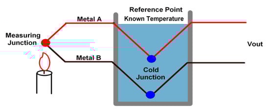
Figure 1.
Thermoelectric converter with two dissimilar metals, explaining the Seebeck principle [14].
A literature review reveals that some attempts have been made to detect a suitable amount of voltage using nanoantenna-coupled thermoelectric converters [20,21,22,23]. An antenna coupled with single and bi-metal nano-thermocouples comprising a dipole antenna and lead nanowires has been introduced [24]. The excitation and dimensions of the design were centered on a 28.3-THz laser source. For (n = 10) series thermocouple connections, the excitation detected 2 µV of voltage. Similarly, a single metal has been used as a thermocouple [25]. By varying the widths of the conductors, the authors were able to achieve simplification in fabrication and the same Seebeck effect, producing similar output voltages as in their previous work.
In this paper, we focus our attention on nanoantenna-coupled thermoelectric sensors for detecting infrared energy. As found in the literature review, only a handful of research groups have considered this technique and there exists a significant opportunity to maximize the results in terms of detecting higher voltages. We utilize gold–nickel combinations as thermoelectric converters and integrate them with nanoantenna designs that follow the Yagi–Uda principle. Electron-beam lithography (EBL) techniques are used to fabricate the proposed nanoantenna designs. The operating principle is the same as that of the Seebeck effect, wherein we excite the nanoantenna designs with various laser wavelengths (650 nm, 940 nm, and 1550 nm) that detect voltages produced by the properties of intersecting materials. Compared to the state of the art, to our knowledge, this is the first time that peak percentage voltage hike detection is attained when utilizing infrared energy [26,27,28,29].
2. Antenna Designs and Simulation
To decide on an optimal design that provides a better response in terms of impedance bandwidth, high gain, and narrow beamwidth, various nanoantenna design topologies that are based on a planar microstrip nature and placed on a silicon substrate were studied [30]. These designs were selected considering the constraints and framework of fabricating tolerances. From the literature review of planar structures, the optimum design was selected to be directional in nature [31] and is presented in Figure 2. The three designs (traditional Yagi–Uda, quasi-Yagi–Uda, and nano-thermoelectric junction) were simulated using commercially available electromagnetic software, CST Microwave Studio [32]. The designs were optimized in such a way that they resonated well at a center frequency of 193.5 THz (1550-nm wavelength). In all three designs, silicon glass (Si + SiO2) was used as a substrate material, with a thickness of 301.2 µm. The conducting elements, gold (Au) and nickel (Ni), were used in designs having a thickness of 0.2 µm. All the nanoantennas presented were a combination of two portions (directors and thermoelectric converters). One portion followed the traditional design scheme of Yagi–Uda, i.e., driven elements, reflectors, and directors, whereas the other portion was the nano-thermoelectric junction. Gold, with its better electron conductivity, was selected for the radiator portion of the design, whereas nickel in conjunction with gold was used in the thermoelectric portion (hot region) of the design.
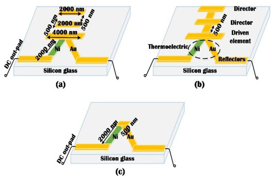
Figure 2.
Proposed nanoantenna designs for this work: (a) Traditional Yagi–Uda, (b) quasi-Yagi–Uda, and (c) nano-thermoelectric junction.
Since the design was tuned to operate in the 193.5-THz band, the electromagnetic (EM) simulator’s optical template was used to correctly model the nanoantenna designs. The material and conduction losses of the substrate and radiating elements, in terms of dielectric constant and loss tangent, were calculated from the Drude model [33], whereas the constants for the Seebeck effect were taken from [34]. The working principle of the Drude model is that it shows how positive and negative ions behave inside any metallic material at the nanoscale level when illuminated with infrared light. The model demonstrates that metals have a massive positive ion from which many free electrons become separated due to delocalization of the valence level of atoms when brought in close proximity to the potential of other interacting atoms. The model also negates long-range interaction among the positive and negative ions while discussing how the interaction is based on instantaneous collisions. The average time associated with these instantaneous collisions of electrons is termed τ, while the velocity and direction of an electron after the collision are dependent on the local temperature distribution [35].
Details gathered from the Drude model and its incorporation into our simulation software, i.e., CST-MWS, were adjusted carefully [36]. Table 1 lists the approximate values of these antenna materials and constants, such as refractive index n, extinction coefficient k, and dielectric permittivity ϵr. All the nanoantennas were excited by a plane wave following the unit cell boundary conditions. The advantage of using the unit cell boundary was that the simulation environment was controlled in terms of mesh assignment, periodic field repetition, and analyzing antenna as a single element while predicting the post-processing results in infinite array structures afterward. Adopting the aforementioned design and simulation criteria, the three designs produced bandwidths in the required frequency range (190–200 THz). Figure 3 depicts the reflection coefficient S11 response of the designs. The maximum bandwidth produced was 4 THz (192–196 THz), which corresponded to a fractional bandwidth of 2.06%.

Table 1.
Optical constants, dielectric permittivity, and Seebeck coefficients for materials at 193.5 THz [33,34].
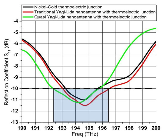
Figure 3.
Reflection coefficient S11 of the three nanoantenna designs tuned at the center frequency of 193.5 THz (simulation).
3. Fabrication Methodology
The process of fabrication is presented in Figure 4. The nanoantennas and the thermoelectric junction sensor were designed simultaneously. A silicon wafer that was previously insolated by a 1-µm-thick silicon wet oxide was used for confirmation. After this step, two different levels of metal were deposited. Due to dimensions and for practical purposes, the micromachining technology chosen was e-beam lithography with a lift-off process. The equipment used was a Xenos lithography module installed on a JEOL 7900 FEG SEM. The e-beam equipment was associated with PMMA (polymethylmethacrylate) electronic photoresist. The PMMA was spin-coated on the silicon wafer to obtain a 1-µm-thick layer (Figure 4a). The e-beam was then directly exposed to the PMMA following the desired design. After electronic exposure, PMMA was developed with the MIBK developer solution (Figure 4b). The obtained patterns in PMMA were then first covered with a Ti-Au (20 nm–180 nm) layer using EBD (electron beam deposition) equipment (Alliance Concept EVA 451) (Figure 4c) and then directly dipped in an acetone bath to remove the PMMA layer, leading to the final Ti-Au patterns (Figure 4d). This lift-off operation was performed again to obtain the Ni layer in the same way as presented in Figure 4e–h.

Figure 4.
Process flow cross-section of nanoantenna fabrication. (a) PMMA (polymethylmethacrylate) was spin-coated on a silicon wafer; (b) e-beam lithography and PMMA development; (c) Ti/Au deposition (20 nm and 180 nm); (d) PMMA lift-off with acetone; (e) PMMA was again spin-coated to cover the design; (f) 2nd e-beam lithography and PMMA development; (g) Ni was deposited in the cavity; (h) PMMA lift-off with acetone.
4. Results and Discussion
Before the proposed nanoantenna designs were illuminated with lasers of various wavelengths, we first focused on the thermoelectric junction to confirm the sensitivity of the detectors. The realized nanoantenna designs are depicted in Figure 5. Thermal analysis to detect output voltage on the proposed design was not performed due to the unavailability of the feature in the utilized commercial electromagnetic simulator (CST-MWS). An initial geometric design of the thermocouple was utilized after a literature review of the available nanoantenna designs [37,38]. The realized thermoelectric junction design depicted in Figure 5c was tested via uniform thermal heating with the experimental setup presented in Figure 6. An Agilent B1500A semiconductor current/voltage characterization system was used to measure the output thermal response via metrics of sweeping, spot heating, sampling, and pulse recording. Electrical contacts were provided by a probe station combined with a microscope. Samples were placed on a thermally monitored chuck. The B1500 was used in sampling mode; the experimental setup consisted of a constant low current (100 pA) in the nanoantenna and the voltage variation was measured.
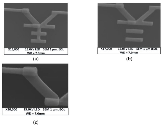
Figure 5.
Obtained nanoantenna prototypes: (a) traditional Yagi–Uda; (b) quasi-Yagi–Uda; (c) nano-thermoelectric junction.
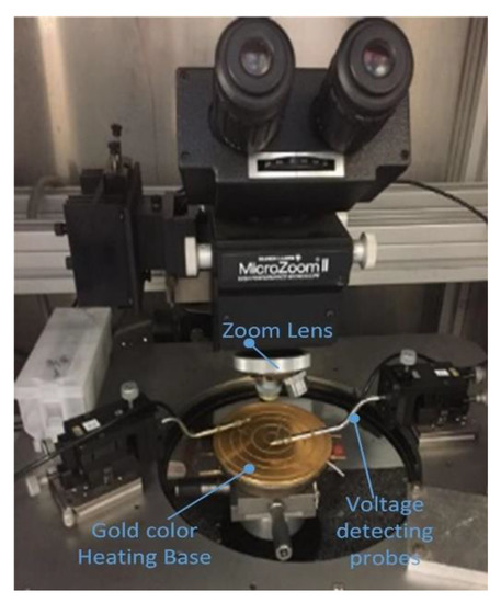
Figure 6.
Experimental setup showing the thermal heating base used to detect voltage hikes of proposed thermoelectric junction design.
Figure 7a shows the results of the thermoelectric junction when heated suddenly and placed on the uniform heating plate seen in Figure 6. This was verified by the results that the proposed thermoelectric junction was reacting to a momentary lapse in thermal gradient appearing at its two sides. It also reacted to several thermal jumps, leading to voltage spikes at each increase in T °C (30–50–80–120 °C).
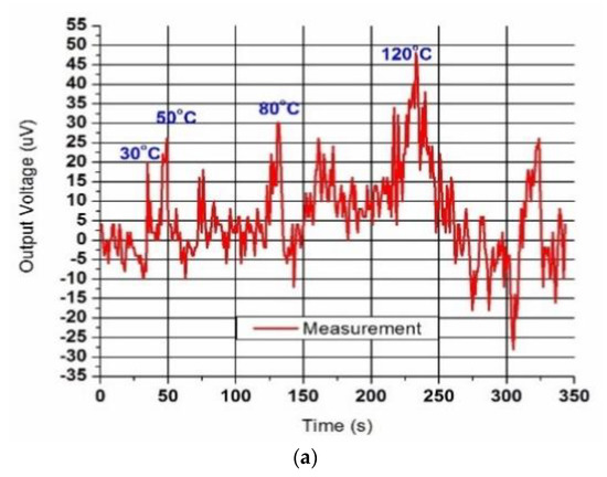
Figure 7.
Peak voltage detection by thermal heating measurements. (a) Results of quick uniform thermal heating (µV); (b) percentage peak voltage detection of (a); (c) percentage voltage detection of a single thermoelectric junction tested with a switch-off smoking lighter, approximately 60 °C at 1 cm of distance.
Each time, a few microvolts of spikes per temperature (20 µV/30 °C, 25 µV/50 °C, 30 µV/80 °C, and 50 µV/120 °C) were seen, which disappeared when thermal equilibrium was obtained between the two sides. Due to the experimental setup using chuck heating for the entire wafer, it was difficult to reach a high level of thermal gradient; therefore, the voltage output was very small. Switching off the heating source resulted in a decreased voltage response, which indicated that the potential difference or maximum temperature between the metals was reached, so the response was lost due to their thermal effect. A more suitable depiction of Figure 7a is presented in Figure 7b in the form of a peak percentage voltage hike. The reference line (noise floor) was set at an average voltage detection and the increase in percentage voltage at different thermal gradients is shown. It can be seen in Figure 7b that, as the temperature was increased, the peak percentage voltage also increased. The minimum increase observed at 30 °C was 20%, whereas the maximum 50% increase was observed at 120 °C for the entire experiment. The voltage spikes then tended to decrease, meaning that the temperature difference between the conducting metals started to decline. Similarly, Figure 7c shows the thermoelectric junction behavior when approaching a heat source (in this case, an approximately 60 °C metal piece coming from a switch-off lighter near the device, i.e., 1 cm). It was observed that the junction reacted directly, leading to an almost 62% increase from the reference detected voltage, having a short life peak (<1 s). The same effect was observed with a zero-level return when thermal equilibrium was reached in the junction.
The next phase of experiments was conducted to test the realized nanoantenna as an infrared detector. To serve this purpose, it was decided that laser sources with numerous wavelengths would be used. This required the use of a tunable laser but, due to unavailability, an in-lab solution was presented. A laser with modulation which had a low square signal of 1 Hz was prepared using a Keysight 33500B series signal generator. A low-frequency signal of around 1 s was used due to the short lifetime of the peak response of our thermoelectric junction. The fabricated nanoantennas were excited via multiple wavelength laser sources of 650 nm (red laser), 940 nm (LED 30 mW/str), and 1550 nm (laser). The output power of each laser source was set to a 5-mW maximum. The output voltage from the nanoantennas, placed inside a special casing, was measured via probes connected to the analyzer, using the experimental setup shown in Figure 8.
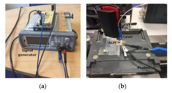
Figure 8.
Experimental devices; (a) square signals generator; (b) testing nanoantenna with laser excitation.
The red laser source operating at 650 nm was the first to be used on the realized nanoantennas. A 50% duty cycle (1-Hz square signal) with a half-second excitation resulted in the results depicted in Figure 9 for the quasi-Yagi–Uda and single thermoelectric junction. The results reveal that the single thermoelectric junction, when excited with the red laser, detected some peak percentage voltage hikes. Heating the junction with metals with different thermal constants gave rise to a positive voltage which declined quickly and was presented as a decreased voltage value of zero as the temperatures among the metals became similar. Halting the excitation caused a further decrease in temperature but with different metal temperatures. Shortly after the excitation was halted, a negative voltage appeared, indicating similar temperatures in the metals and resulting in a voltage drop to zero.
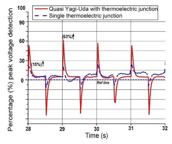
Figure 9.
Influence of 650-nm laser pulses on quasi-Yagi–Uda nanoantenna and thermoelectric junction design in terms of voltage response.
According to Figure 9, it appears that the single thermoelectric junction detected a smaller peak percentage voltage hike than the thermoelectric junction combined with the quasi-Yagi–Uda nanoantenna. When the single thermoelectric junction delivered a 15% voltage hike, the adjunction of the nano quasi-Yagi–Uda device was able to provide an almost four-times higher peak. For a 650-nm pulse excitation, the maximum recorded voltage increase was around 63%. Likewise, for the 940-nm excitation source, the nanoantenna detected a voltage increase of 92% compared to the reference voltage. Figure 10 depicts the measured results. Differences in peak percentage detected voltages could result from the input laser energy but also from the beam size of the laser, which was much wider in the case of the 940-nm excitation source (diode delivering 30 mW/str). The main objective of the study was to evaluate the sensing effect at different wavelengths.
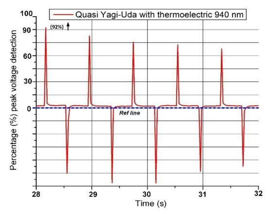
Figure 10.
Influence of 940-nm laser pulses on quasi-Yagi–Uda nanoantenna design in terms of voltage response.
An array form of the proposed thermoelectric junction and traditional Yagi–Uda nanoantenna was fabricated to test the design with a final laser excitation source of 1550-nm wavelength. The nanoantennas were wire-bonded on an integrated chip, while the probes used earlier were omitted from the electrical testing. Figure 11 depicts the three realized designs on silicon substrate for measurement at 1550-nm laser excitation along with the wire-bonded arrangement. The realized elements include a single quasi-Yagi–Uda design along with 1 × 5 array elements of the traditional Yagi–Uda and thermoelectric junction. The measured results of the three designs are presented in Figure 12, with the relevant data tabulated in Table 2. Analysis of the results shows that the maximum peak percentage voltage hike produced by the single quasi-Yagi–Uda element is 28%, while the thermoelectric array produced 55% and the traditional Yagi–Uda array produced around 80% in comparison to the reference nanoantenna depicted in Figure 7a. As demonstrated by earlier excitation results, the positive voltage or peaks appeared due to the thermal difference among the metals, while the negative voltage appeared when the heating source was halted or a discharging effect occurred between the metals. The experiments were successfully conducted, and results were accurately achieved with the assistance of the NanoRennes platform supported by the Renatech network (CNRS) at IETR, University of Rennes 1, France. Table 3 compares our results with similar nanoantenna designs in the literature which are intended for infrared energy detection and to produce certain output voltages. It can be seen that our proposed design produces an output voltage that is far superior to the others, although we acknowledge that the works of other authors offer greater design simplicity.
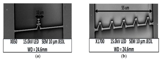
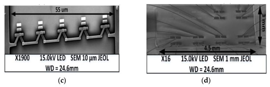
Figure 11.
Realized structures for 1550-nm laser excitation: (a) Quasi-Yagi–Uda; (b) array of the nano-thermoelectric junction; (c) array of traditional Yagi–Uda; (d) zoomed out image of the nanoantenna chip showing the wire-bonding.
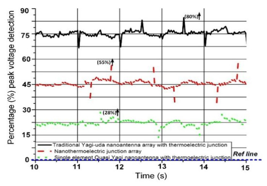
Figure 12.
Measurement: excitation of the three designs with a 1550-nm laser.
Table 2.
Comparison of the peak percentage voltage hikes shown in Figure 12 when excited with a 1550-nm laser source.
Table 3.
Comparison with similar nanoantenna designs for detecting infrared energy.
5. Conclusions
In this study, we experimentally demonstrated the effect of thermal infrared heating on nanoantennas. Three nanoantenna designs were presented and realized for resonance in the optical C-band (1550 nm). The nanoantenna designs involved the integration of thermoelectric sensors made from Au and Ni and the Yagi–Uda structures. The simulation of the three designs was performed by CST-MWS and resonated well at the center wavelength. The open-circuit voltage was calculated by the known Seebeck effect. This technique involved the fabrication and testing of various nanoantenna designs. The excitation was provided with three optical wavelength sources, i.e., 650, 940, and 1550 nm. The designs were responsive to the three excitation pulses as peak percentage voltage hikes were noted. It was found that the quasi-Yagi–Uda nanostructure combined with a thermoelectric junction detected four-times more voltage hikes than the single thermoelectric junction. For the single-element quasi-Yagi–Uda nanoantenna, the nano thermoelectric junction array, and the array of traditional Yagi–Uda nanoantennas, excitation with a 1550-nm laser-produced 28%, 55%, and 80% peak high voltages, respectively. It is important to note that the results produced in terms of voltage with various wavelengths were mostly qualitative-based results rather than quantitative among wavelengths. From our results, we conclude that practical infrared energy detection is possible for small electronics, but for higher and more stable output voltages, future work on better antennas, thermocouples, and array designs will be directed toward this goal.
Author Contributions
Conceptualization, W.T.S., M.H. and H.V.; Data curation, W.T.S. and O.D.S.; Formal analysis, M.H.; Funding acquisition, S.A.A.; Investigation, W.T.S., O.D.S. and M.H.; Methodology, H.V.; Project administration, S.A.A.; Resources, O.D.S., M.H., H.V. and S.A.A.; Software, W.T.S.; Supervision, H.V.; Validation, W.T.S., O.D.S., M.H. and S.A.A.; Writing—original draft, W.T.S.; Writing—review and editing, H.V. All authors have read and agreed to the published version of the manuscript.
Funding
This work was supported by the Researchers Supporting Project number (RSP-2020/46), King Saud University, Riyadh, Saudi Arabia.
Data Availability Statement
Data available upon request from authors.
Conflicts of Interest
The authors declare no conflict of interest.
References
- Howell, J.R.; Menguc, M.P.; Siegel, R. Thermal Radiation Heat Transfer; CRC Press: Boca Raton, FL, USA, 2015. [Google Scholar]
- Guan, Q.; Yin, X.; Guo, X.; Wang, G. A novel infrared motion sensing system for compressive classification of physical activity. IEEE Sens. J. 2016, 16, 2251–2259. [Google Scholar] [CrossRef]
- Bean, J.A.; Tiwari, B.; Szakmány, G.; Bernstein, G.H.; Fay, P.; Porod, W. Antenna length and polarization response of antenna-coupled MOM diode infrared detectors. Infrared Phys. Technol. 2010, 53, 182–185. [Google Scholar] [CrossRef]
- Caniou, J. Passive Infrared Detection: Theory and Applications; Springer Science and Business Media: Berlin/Heidelberg, Germany, 2013. [Google Scholar]
- Abbasi, Q.H.; Alomainy, A.; Jornet, J.M.; Han, C.; Chen, Y. Ieee Access Special Section Editorial: Nano-Antennas, Nano-Transceivers and Nano-Networks/Communications. IEEE Access 2018, 6, 8270–8272. [Google Scholar] [CrossRef]
- Nouri-Novin, S.; Sadatgol, M.; Zarrabi, F.B.; Bazgir, M. A hollow rectangular plasmonic absorber for nano biosensing applications. Optik 2019, 176, 14–23. [Google Scholar] [CrossRef]
- Sethi, W.T.; De Sagazan, O.; Vettikalladi, H.; Fathallah, H.; Himdi, M. Yagi-Uda nantenna for 1550 nanometers optical communication systems. Microw. Opt. Technol. Lett. 2018, 60, 2236–2242. [Google Scholar] [CrossRef]
- Barreda, A.I.; Saleh, H.; Litman, A.; González, F.; Geffrin, J.M.; Moreno, F. Scattering directionality of high refractive index dielectric particles: A note for solar energy harvesting. Physics, Simulation, and Photonic Engineering of Photovoltaic Devices VII. Int. Soc. Opt. Photonics 2018, 10527, 105270. [Google Scholar] [CrossRef]
- Chen, Y.; Ding, F.; Coello, V.; Bozhevolnyi, S.I. On-Chip Spectropolarimetry by Fingerprinting with Random Surface Arrays of Nanoparticles. ACS Photon 2018, 5, 1703–1710. [Google Scholar] [CrossRef]
- Jayaswal, G.; Belkadi, A.; Meredov, A.; Pelz, B.; Moddel, G.; Shamim, A. A Zero-Bias, Completely Passive 28 THz Rectenna for Energy Harvesting from Infrared (Waste Heat). In Proceedings of the 2018 IEEE/MTT-S International Microwave Symposium—IMS, Philadelphia, PA, USA, 10–15 June 2018; IEEE: Piscataway, NJ, USA, 2018; pp. 355–358. [Google Scholar]
- El-Toukhy, Y.M.; Hussein, M.; Hameed, M.F.O.; Heikal, A.M.; Abd-Elrazzak, M.M.; Obayya, S.S.A. Optimized tapered dipole nanoantenna as efficient energy harvester. Opt. Express 2016, 24, A1107–A1122. [Google Scholar] [CrossRef]
- Yan, S.; Tumendemberel, B.; Zheng, X.; Volskiy, V.; VandenBosch, G.A.; Moshchalkov, V.V. Optimizing the bowtie nano-rectenna topology for solar energy harvesting applications. Sol. Energy 2017, 157, 259–262. [Google Scholar] [CrossRef]
- Jayaswal, G.; Belkadi, A.; Meredov, A.; Pelz, B.; Moddel, G.; Shamim, A. Optical rectification through an Al2O3 based MIM passive rectenna at 28.3 THz. Mater. Today Energy 2018, 7, 1–9. [Google Scholar] [CrossRef]
- Yang, Y.; Zhang, H.; Zhu, G.; Lee, S.; Lin, Z.-H.; Wang, Z.L. Flexible Hybrid Energy Cell for Simultaneously Harvesting Thermal, Mechanical, and Solar Energies. ACS Nano 2013, 7, 785–790. [Google Scholar] [CrossRef] [PubMed]
- Wang, J.X.; Wang, X.L. Application and Development of Thermostat on Thermocouple Temperature Measurement. Available online: https://en.cnki.com.cn/Article_en/CJFDTotal-DILY200805022.htm (accessed on 26 July 2020).
- Sarma, U.; Boruah, P. Design and development of a high precision thermocouple based smart industrial thermometer with on line linearisation and data logging feature. Measurement 2010, 43, 1589–1594. [Google Scholar] [CrossRef]
- Alekseev, S.; Ziskin, M. Distortion of millimeter-wave absorption in biological media due to presence of thermocouples and other objects. IEEE Trans. Biomed. Eng. 2001, 48, 1013–1019. [Google Scholar] [CrossRef]
- Neikirk, P.D.; Rutledge, D.B. Self-heated thermocouples for far-infrared detection. Appl. Phys. Lett. 1982, 41, 400–402. [Google Scholar] [CrossRef][Green Version]
- Atkeson, P.L.C. Thermocouple-Triggered Igniter. U.S. Patent 5,166,468, 24 November 1992. [Google Scholar]
- Mendez-Lozoya, J.; de León-Zapata, R.D.; Guevara, E.; González, G.; González, F.J. Thermoelectric efficiency optimization of nanoantennas for solar energy harvesting. J. Nanophotonics 2019, 13, 026005. [Google Scholar] [CrossRef]
- Ghanim, A.; Hussein, M.; Hameed, M.F.O.; Obayya, S.S.A. Design considerations of super-directive nanoantennas for core-shell nanowires. J. Opt. Soc. Am. B 2017, 35, 182–188. [Google Scholar] [CrossRef]
- Zhao, H.; Gao, H.; Li, B. Theory and method for large electric field intensity enhancement in the nanoantenna gap. Appl. Opt. 2019, 58, 670–676. [Google Scholar] [CrossRef] [PubMed]
- Mahmoud, K.R.; Hussein, M.; Hameed, M.F.O.; Obayya, S.S.A. Super directive Yagi–Uda nanoantennas with an ellipsoid reflector for optimal radiation emission. J. Opt. Soc. Am. B 2017, 34, 2041. [Google Scholar] [CrossRef]
- Szakmany, G.P.; Orlov, A.O.; Bernstein, G.H.; Porod, W. Polarization-dependent response of single-and bi-metal antenna-coupled thermoelectrics for infrared detection. IEEE Trans. Terahertz Sci. Technol. 2015, 6, 884–891. [Google Scholar] [CrossRef]
- Russer, J.A.; Jirauschek, C.; Szakmany, G.P.; Orlov, A.O.; Bernstein, G.H.; Porod, W.; Lugli, P.; Russer, P. Antenna-coupled terahertz thermocouples. In Proceedings of the 2015 IEEE MTT-S International Microwave Symposium, Phoenix, AZ, USA, 17–22 May 2015; pp. 1–4. [Google Scholar] [CrossRef]
- Mubarak, M.H.; Sidek, O.; Abdel-Rahman, M.; Mustaffa, M.T.; Kamal, A.S.M.; Mukras, S.M.S. Nano-antenna coupled infrared detector design. Sensors 2018, 18, 3714. [Google Scholar] [CrossRef] [PubMed]
- Ngo, H.D.; Chen, K.; Ørjan, H.S.; Doan, A.T.; Ngo, T.D.; Dao, T.D.; Ikeda, N.; Ohi, A.; Nabatame, T.; Nagao, T.; et al. Nanoantenna structure with mid-infrared plasmonic niobium-doped titanium oxide. Micromachines 2019, 11, 23. [Google Scholar] [CrossRef]
- Briones, E.; Ruiz-Cruz, R.; Briones, J.; Simon, J. Optimization of Seebeck nanoantenna-based infrared harvesters. Opt. Express 2019, 28, 116. [Google Scholar] [CrossRef] [PubMed]
- Chekini, A.; Neshat, M.; Sheikhaei, S. Infrared rectification based on electron field emission in nanoantennas for thermal energy harvesting. J. Mod. Opt. 2019, 67, 179–188. [Google Scholar] [CrossRef]
- Pinho, P. Optical Communication Technology; BoD–Books on Demand: Norderstedt, Germany, 2017. [Google Scholar]
- Taminiau, T.H.; Stefani, F.D.; van Hulst, N.F. Enhanced directional excitation and emission of single emitters by a nano-optical Yagi-Uda antenna. Opt. Express 2008, 16, 10858–10866. [Google Scholar] [CrossRef]
- Computer Simulation Technology Version 2019. Available online: https://www.3ds.com/products-services/sim-ulia/products/cst-studio-suite/ (accessed on 10 June 2020).
- Johnson, P.B.; Christy, R.W. Optical constants of the noble metals. Phys. Rev. B 1972, 6, 4370–4379. [Google Scholar] [CrossRef]
- Hoque, A.; Islam, M.T.; Almutairi, A.F.; Alam, T.; Singh, M.J.; Amin, N. A polarization independent quasi-TEM Metamaterial absorber for X and Ku band sensing applications. Sensors 2018, 18, 4209. [Google Scholar] [CrossRef] [PubMed]
- Capolino, F. Applications of Metamaterials; CRC Press: Boca Raton, FL, USA, 2017. [Google Scholar]
- Episkopou, E.; Papantonis, S.; Otter, W.J.; Lucyszyn, S. Defining material parameters in commercial EM solvers for arbitrary metal-based THz structures. IEEE Trans. Terahertz Sci. Technol. 2012, 2, 513–524. [Google Scholar] [CrossRef]
- Wei, J.; Ren, Z.; Lee, C. Metamaterial technologies for miniaturized infrared spectroscopy: Light sources, sensors, filters, detectors, and integration. J. Appl. Phys. 2020, 128, 240901. [Google Scholar] [CrossRef]
- Szentpáli, B.; Matyi, G.; Fürjes, P.; László, E.; Battistig, G.; Bársony, I.; Károlyi, G.; Berceli, T. Thermoelectric-based THz antenna. Microsyst. Technol. 2012, 7, 849–856. [Google Scholar]
- Feng, L.; Lee, J.; Jiang, A.; Jung, S.; Belkin, M.A. Thermoelectric detector of light ellipticity. Nat. Commun. 2016, 7, 12994. [Google Scholar]
- Shimizu, Y.; Mizoshiri, M.; Mikami, M.; Ito, Y.; Sakurai, J.; Hata, S. Fabrication of flexible thermoelectric generators with a lens array for near-infrared solar light harvesting. In Proceedings of the 2015 IEEE MTT-S International Microwave Symposium, Belfast, UK, 21–25 January 2018. [Google Scholar]
- Szakmany, G.P.; Orlov, A.O.; Bernstein, G.H.; Porod, W. Nanoantenna arrays for infrared detection with single-metal nanothermocouples. Infrared Phys. Technol. 2017, 82, 44–49. [Google Scholar] [CrossRef]
- He, M.; Lin, Y.-J.; Chiu, C.-M.; Yang, W.; Zhang, B.; Yun, D.; Xie, Y.; Lin, Z.-H. A flexible photo-thermoelectric nanogenerator based on MoS2/PU photothermal layer for infrared light harvesting. Nano Energy 2018, 49, 588–595. [Google Scholar] [CrossRef]
Publisher’s Note: MDPI stays neutral with regard to jurisdictional claims in published maps and institutional affiliations. |
© 2021 by the authors. Licensee MDPI, Basel, Switzerland. This article is an open access article distributed under the terms and conditions of the Creative Commons Attribution (CC BY) license (http://creativecommons.org/licenses/by/4.0/).