Article

Suppressing Voltage Spikes of MOSFET in H-Bridge Inverter Circuit

by
Ezzidin Hassan Aboadla
1,2,*,
Sheroz Khan
3,*,
Kushsairy Abdul Kadir
1,*,
Zulkhairi Md Yusof
1,
Mohamed Hadi Habaebi
4,
Shabana Habib
5,
Muhammad Islam
3,
Mohammad Kamrul Hasan
6 and
Eklas Hossain
7
1
Electrical Technology Section, British Malaysian Institute, University Kuala Lumpur, Batu 53100, Malaysia
2
Electrical and Electronics Department, Higher Institute of Science and Technology, Al-Zahra 47760, Libya
3
Department of Electrical and Renewable Energy Engineering, College of Engineering and Information Technology, Unaizah Colleges, Al-Qassim 51911, Saudi Arabia
4
Electrical and Computer Engineering Department, International Islamic University Malaysia, Jalan Gombak 53100, Malaysia
5
Department of Information Technology, College of Computer, Qassim University, Buraydah 51452, Saudi Arabia
6
Center for Cyber Security, Universiti Kebangsaan Malaysia, Bangi 43600, Malaysia
7
Oregon Renewable Energy Center (OREC), Department of Electrical Engineering & Renewable Energy, Oregon Institute of Technology, Klamath Falls, OR 97601, USA
*
Authors to whom correspondence should be addressed.
Electronics 2021, 10(4), 390; https://doi.org/10.3390/electronics10040390
Submission received: 6 January 2021 / Revised: 29 January 2021 / Accepted: 1 February 2021 / Published: 5 February 2021

Abstract

:
Power electronics devices are made from semiconductor switches such as thyristors, MOSFETs, and diodes, along with passive elements of inductors, capacitors, and resistors, and integrated circuits. They are heavily used in power processing for applications in computing, communication, medical electronics, appliance control, and as converters in high power DC and AC transmission in what is now called harmonized AC/DC networks. A converter’s operation is described as a periodic sequencing of different modes of operation corresponding to different topologies interfaced to filters made of passive elements. The performance of converters has improved considerably using high switching frequency, which leads to a significant improvement in a power converter’s performance. However, the high dv/dt through a fast-switching transient of the MOSFET is associated with parasitic components generating oscillations and voltage spikes having adverse effects on the operation of complementary switches, thereby affecting the safe operation of the power devices. In this paper, the MOSFET gate-driver circuit performance is improved to suppress the H-Bridge inverter’s voltage spikes. The proposed technique is a simple improvement to the gate driver based on the IR2112 driver (IC) by adding a capacitor to attenuate the effect of parasitic components and the freewheeling current, suppressing the negative voltage spikes. This paper’s main contribution is to improve the gate driver circuit’s capability for suppressing the voltage spikes in the H-Bridge inverter. The improved gate driver circuit is validated experimentally and is compared with the conventional gate driver. The experimental results show that the proposed technique can effectively suppress the MOSFET’s voltage spikes and oscillations.

1. Introduction

Producing high-quality output waveforms from Multilevel Inverter (MLI) has been challenging for researchers working in the area. The high-quality output results from reduced switching losses in the power semiconductors and for improving output waveform [1,2,3,4]. With the rapid development of the power transistor industry, fast switching frequency speed has greatly increased. Although higher switching frequency guarantees quality output, it increases switching losses. However, by applying high switching speed, the parasitic parameters such as parasitic capacitance and inductance with the PCB traces become crucial factors that mainly affect the power transistors’ performance. Therefore, it is important to analyze these parasitic components’ effect and calculate the loss of the MOSFET accurately. One has to engage in a tradeoff between the two situations when it comes to implementing power converters. On the other hand, H-Bridge inverters have suffered from voltage spikes in their output signals. These spikes have undesirable effects such as phonetic noise and harmonic heating losses, semiconductors switching power losses, and mechanical vibrations [5,6]. On the other hand, the parasitic inductance can boost the voltage overshoot, leading to total harmonic distortion. It is important to eliminate the parasitic resonance to improve the H-Bridge converter’s performance and mitigate the effect of the total harmonic distortion [7]. A root locus technique has been used with an RC snubber circuit design in Reference [8] for a double pulse circuit of the SiC MOSFET by ignoring the parasitic inductance source. Simultaneous switching of these devices can generate a high voltage spike and high dv/dt at the inverters’ output terminal. This high voltage spike may easily damage the power switches. In practical operation of H-Bridge converter during ON/OFF transient of one MOSFET under fast switching conditions will produce voltage spikes on its complementary MOSFET [9,10,11,12,13,14]. Several techniques have been used to suppress the effect of voltage spikes [15,16]. Reference [17] proposed controlled gate resistance to mitigate the voltage spikes. However, it needs to use feedback control, which leads to a relative time delay. A level shift circuit is proposed in Reference [18] to produce a negative gate voltage to suppress the positive gate spikes; however, this negative gate voltage considers a risk to damage the MOSFET. In [19,20,21,22,23], Snubber circuits have been utilized with semiconductor devices to absorb the high dv/dt energy and reduce harmonic spikes. The voltage spikes will increase due to the reverse load current by increasing the load current [24]. Developing a gate driver of SiC MOSFET will eliminate the gate-source voltage spike. A series of capacitors have been connected to the gate of a MOSFET transistor by an auxiliary transistor to absorb the negative voltage spike when the complementary power transistor is turned off [25]. In [26], a new active driver circuit is proposed for the MOSFET transistor to absorb the effect of turn-off spikes and oscillation. Another technique is proposed to reduce positive voltage spikes by using an auxiliary transistor for controlling JFET. However, this technique cannot mitigate negative voltage spikes [27]. The soft gate technique and active driver-controlled circuit are presented in Reference [28]. A novel technique for the driver gate controller to suppress the negative voltage spikes is introduced in Reference [29]. In the turn off state and due to the voltage rising across the MOSFET, charging current stream via its parasitic capacitance leads to inducing positive voltage spikes at the gate. If the voltage of these spikes overrun gate threshold voltage, the high side of the MOSFET could be falsely triggering. The gate impedance monitoring method has been used to decrease the gate voltage spikes in order to provide a low impedance path by added external gate-source capacitance [30,31]
This paper presents a new design to suppress the voltage spikes by improving the MOSFET gate driver circuit in the H-Bridge circuit based on the integrated circuit IR2112. The performance of the proposed technique has been evaluated experimentally.

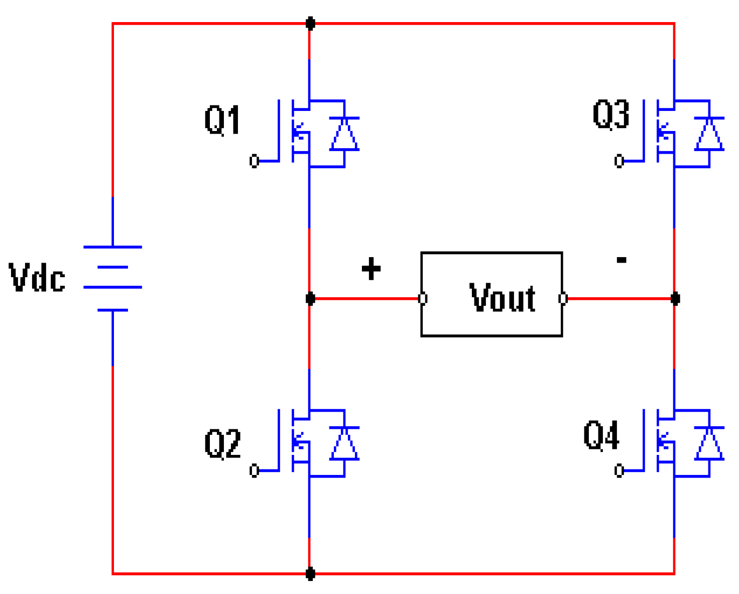
2. H-Bridge Inverter

The H-Bridge inverter is the most common inverter used to convert DC to AC, as shown in Figure 1. Two power switches in a complementary manner are used in each leg of the H-Bridge circuit, which can be controlled (ON/OFF) using modulation signals such as Sinusoidal Pulse Width Modulation (SPWM) or Selective Harmonic Elimination (SHE) technique [32,33]. Each H-Bridge topology unit can generate three-level output voltages, +Vdc, 0, and −Vdc.

3. Proposed Technique
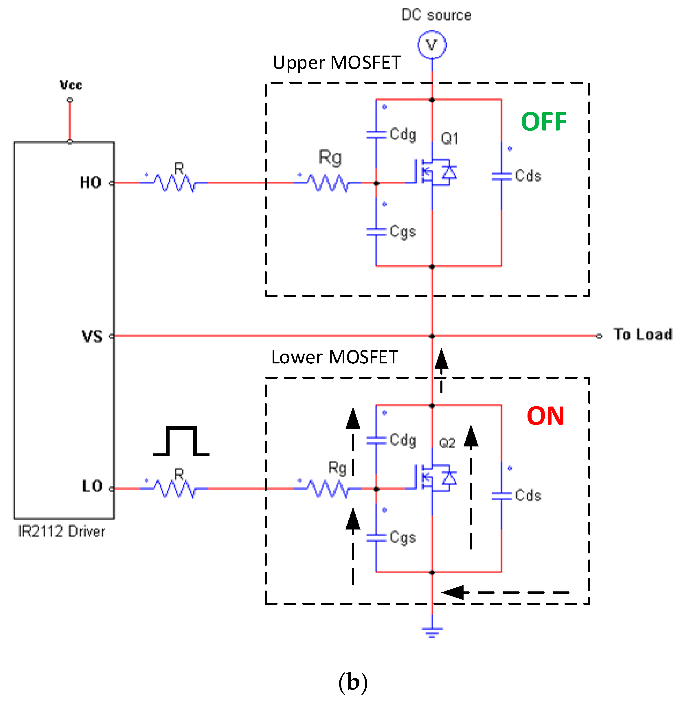
In power switching applications, switching losses at most are dependent on switching speed. Thus, the switching characteristic is the most important in the high-power switching application. In addition, a voltage spike is a very significant issue that affects the performance of the power inverter adversely, and it is presented and addressed in this paper using the proposed approach to design and improved high-performance gate drive circuits based on the gate driver IR2112 for high-efficiency and high-power, switching applications using a power MOSFET and IGBT.

Operating Principle

Figure 2 shows the circuit diagram of the half-bridge circuit with driver IR2112, which drives the power transistors. This integrated circuit has a high-performance and high voltage driver for power switches with two independent channels for high side and low side output. By adding an external bootstrap capacitor (CBOOT) and bootstrap diode (DBOOT), the driver provides a high switching speed [34]. The High Side Floating Voltage (VS) of the IR2112 driver is already connected to the output via the upper transistor source (Q1). When the low side channel (LO) is turned ON, the lower MOSFET (Q2) will be ON, and the high side (HO) turned OFF, the upper MOSFET (Q1) will be OFF. In this case, the VS pin will get connected to the ground via a lower transistor (Q2). The CBOOT capacitor starts charging up via the DBOOT from the VCC source, as shown in Figure 3. [35]. The highest voltage charges from CBOOT are dependent on the voltage value of the VCC source. The equivalent schematic of the MOSFET parasitic components in a half-bridge circuit is shown in Figure 4.
This circuit’s biggest issue is the negative voltage spike existent at the switching device source during the OFF state that causes load current flow suddenly in the low-side freewheeling diode. This negative spike can defect the gate driver’s output because it directly affects the source VS pin of the driver or PWM control IC and might pull some of the internal circuitry significantly below ground, as shown in Figure 5. The other problem caused by the negative voltage transient is developing an over-voltage condition across the bootstrap capacitor. Given the fast-rising drain-source voltage, the parasitic capacitances of a MOSFET cause a negative voltage spike during switching transitions and may result in spurious turn-on if it exceeds the threshold voltage. When the upper MOSFET turns ON, the current flow between the drain and source leads to induce the parasitic capacitor Cdg in the lower MOSFET, and it will motivate the gate-source capacitor Cgs to charge up. Therefore, it will push up the lower MOSFET’s gate voltage and generate a positive pseudo pulse. On the other side, when the lower MOSFET is turned ON, and the upper switch is turned OFF, a negative pseudo voltage will generate between the lower MOSFET gate and source, as shown in Figure 6 [36].
When the power source Vcc of the driver is referenced to the ground, the maximum voltage that can build on the CBoot capacitor is the sum of Vcc and the amplitude of the negative voltage at VS pin. Figure 7 illustrates the waveforms of the high-side MOSFET during the OFF state. The negative voltage spike’s amplitude is proportional to the parasitic inductances and the turn-off speed, di/dt. Sum of Cgs and Cgd, called Miller capacitance. The biggest problem is when the VS goes below ground significantly, and therefore, the gate drive suffers damage.

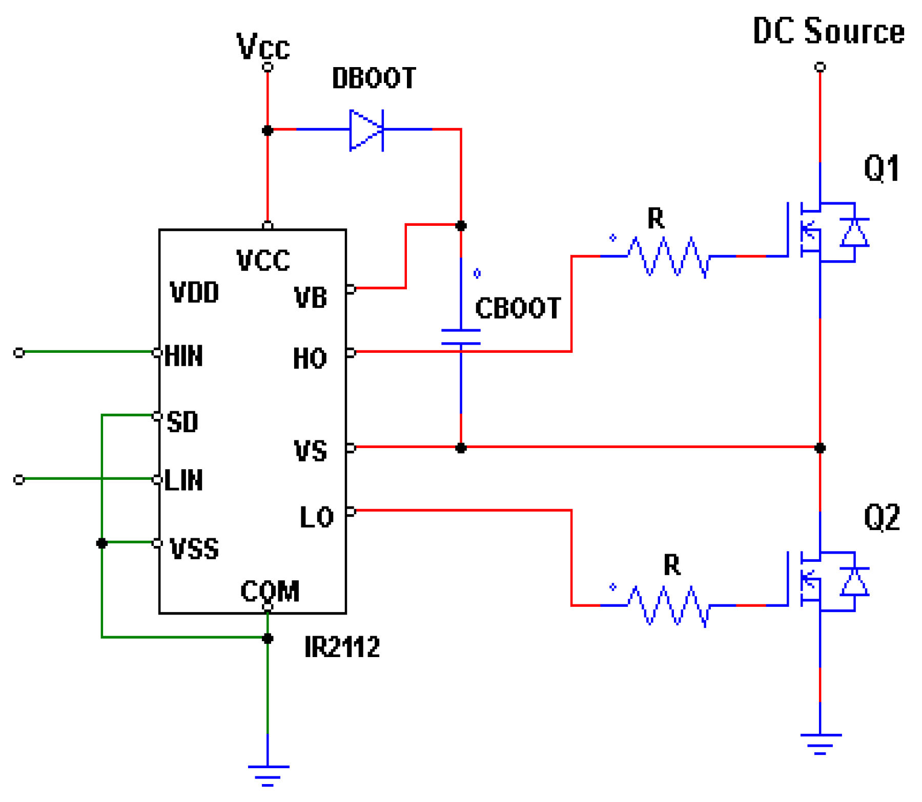
4. Proposed Design to Suppress Voltage Spikes

The proposed design is used to reduce dv/dt at the power switches’ transition and suppress the voltage spikes from the output voltage signal. The gate driver circuit is based on the integrated circuit IR2112. The driver connects to the H-Bridge inverter’s power transistor via three terminals: Ho_ gate signal of the upper transistor, Lo_ gate signal of the lower transistor, and VS feedback signal between the source of the top transistor and the drain of the lower transistor.
When the upper MOSFET is turned OFF and the lower MOSFET is turned ON, the VS pin connection will be connected to the ground via a lower transistor. Therefore, most of the load current (freewheel current) will flow suddenly through the lower MOSFET’s internal diode. Hence, a negative voltage spike will appear at VS-pin, as shown in Figure 8. This negative spike will develop across the CBOOT capacitor, reaching maximum amplitude as the sum of VCC source and the negative spike’s amplitude. At the same time, part of the load current will flow through the parasitic gate-source capacitance Cgs of the lower transistor Q2, which leads to charge the capacitor Cgs. In this case, the gate voltage will push up and generate another harmful gate-source spurious voltage pulse. The voltage spikes issue has occurred during the transient process of the complementary switches of the H-Bridge inverter. The voltage spikes’ value depends on the source voltage and ON time of the duty cycle.
To give the mathematical modeling of the voltage spikes and oscillation conditions, the turn off process of the MOSFET has been analyzed depending on Figure 9. An ideal MOSFET transistor consists of a gate-drain capacitance (Cgd), drain-source capacitance (Cds), gate-source capacitance (Cgs), and internal diode with the parasitic inductance (LD, LS). However, Rg is the gate driver resistance. During turn-off condition of the MOSFET, Cgs capacitance starts discharge via Rg resistance, leading to decreased gate-source voltage Vgs.
Therefore, the pseudo-gate-source voltage of the MOSFET can be based on Reference [25]:
i C g s = C g s d V C g s d t
i C d g = C d g d V C d g d t
V s = V C g s + V C d g
where: C g s ,   C d g ,   C d s   M O S F E T   p a r a s i t i c   c a p a c i y a n c e ; V C g s is the maximum charge value of the C g s capacitor, and V C d g is the maximum charge value of the C d s capacitor.
V C g s ( m a x ) = V s 1 + C g s / C d g
While the drain current id starts falling, the load current moves out to the freewheeling diode (FWD), as illustrated in Equations (5) and (6). Additional to the voltage spikes, the drain current id composes oscillation due to the parasitic components of the MOSFET in the power loop at turn-off operation [26].
i d = g m ( V g s V t h )
d i d d t = g m d V g s d t
where: i d is the drain current; g m is the transconductance.
These issues of voltage spikes will affect the MOSFET through their gate signals. The spikes’ entrance into the circuit may lead to the failure of the switches and damage to the IC driver. Besides, these spikes will show up on the output voltage waveform of the inverter. They may create more problems to the load in the form of electromagnet interference and harmonic-related heating effects.
To tackle the issue of a negative voltage spike, a new capacitor CA is added to the driver IR2112 between VS-pin and the ground to absorb these spikes effectively, as shown in Figure 10. This capacitor’s main objective is to suppress the negative voltage spike, which appears at VS pin of IR2112, to improve the output voltage signal’s quality and reduce voltage spikes.
This capacitor CA provides a low impedance loop to the reverse load current during the transient condition of the upper transistor, leading to suppressing the voltage spikes. At OFF state (when Q1 is OFF), VS pin is connected to the ground via Q2. However, at the ON state (Q1 is ON), the voltage of VS equals the DC source’s voltage, and the voltage-time of this point depends on the duty cycle of PWM. The equivalent circuit of the proposed scheme at the turn off state is shown in Figure 11. Therefore, the new capacitor CA value can be calculated depending on the DC voltage source and ton of the duty cycle.
According to Kirchhoff’s voltage law (KVL) gives:
V L D + V L S + V C d s = V S
L D d i d t + L S d i d t + 1 C d s   i d t = V S
( L D + L S ) d i d t + 1 C d s   i d t = V S
Applying a Laplace transform and solving the differential equation,
S ( L D + L S ) I ( S ) + 1 S C d s I ( S ) = V S ( S )
S 2 [ ( L D + L S ) C d s + 1 ] I ( S ) = V S ( S )
V S = 1 C A   i d t
C A = 1 V S t 1 t 2   i d t ,   t = t o n
where:
  • t1 and t2 is the ON time at the period time of PWM; LD MOSFET Internal Drain Inductance;
  • LS is the Internal Source Inductance; CA is the external capacitor; VS is the voltage at VS pin.
t 1 , 2 = α 1 f s 360
where: fs is the switching frequency.

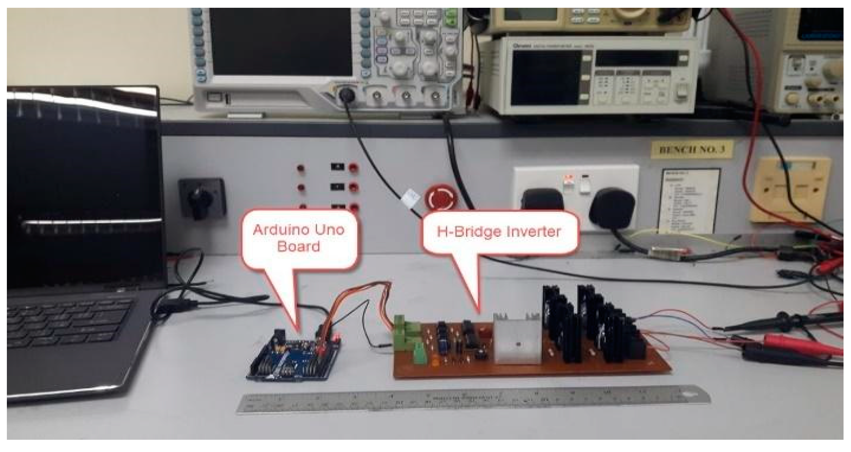
5. Experimental Verification

The proposed gate driver circuit was implemented and tested for the H-Bridge inverter, where the inductive load was utilized to verify the proposed design’s effectiveness for the suppression of the voltage spike and oscillation, as shown in Figure 12. In the experimental prototype, MOSFET IRF640 and IC driver IR2112 were used. An Arduino Uno board was used to generate PWM. The experimental parameters of the design circuit are listed in Table 1.

6. Experimental Results

A 50 Hz and 10 kHz switching frequency was used to operate the inverter circuit to address the effect of negative voltage spikes and the oscillation of the H-Bridge inverter of renewable energy application.

6.1. 50 Hz Switching Results

Figure 13 shows the negative spike at VS pin in a conventional gate drive circuit before using the proposed design. It can be seen that the voltage of the negative spike at V-Spike is 2.5 V.
The gate-source voltage and the drain-source voltage signals for a conventional gate drive circuit and the proposed driver circuit are shown in Figure 14 and Figure 15. Comparing the results of Figure 14 and Figure 15, after improving the driver circuit, the oscillation and the voltage spike amplitude have been mitigated from 10.40 V to 1.50 V.

6.2. 10 KHz Switching Frequency

By using 10 kHz as a switching frequency for the H-Bridge DC to AC inverter, Figure 16 shows the signal at VS pin during OFF state for conventional gate drive.
Figure 16 shows that the negative voltage spike at switching frequency 10 kHz is less than when the switching frequency is 50 Hz with 2.22 V and 2.50 V, respectively. The gate-source voltage Vgs and drain-source voltage Vds waveform are shown in Figure 17 under switching frequency fs = 10 kHz. The voltage spike is raised to 13 V with high oscillation for the drain-source voltage. By increasing the switching frequency, the voltage spikes and the overshoot oscillation are increased on drain-source voltage Uds. However, the negative voltage spike at VS pin is decreased when the switching frequency increases.
The experimental prototype in Figure 10 has been utilized to verify the proposed scheme’s effect for the output voltage waveform of the H-Bridge inverter. Figure 18 illustrates the output voltage waveform with the conventional gate driver circuit before improving the driver. The output voltage signal is affected by the positive and negative voltage spikes, which lead to more issues for power transistors and the load system.
On the other hand, the proposed scheme’s performance for mitigating the voltage spikes of the output voltage waveform of the H-Bridge is presented in Figure 19. In the proposed design, both the positive and negative voltage spikes have been removed from the output voltage signal to a considerably good level.

7. Comparison of MOSFET Gate Driver Techniques for Suppressing Voltage Spikes

A comparison with different methods is presented in References [13,14,15,16,17] to show the proposed scheme’s advantage. These techniques can improve the performance on some sides. However, they all have some disadvantages in other aspects. Table 2 illustrates the comparison between different techniques for the capability of suppressing voltage spikes. This paper’s proposed method has superior characteristics compared to other gate drivers in terms of the voltage spikes suppression capability and the simplicity in design.

8. Conclusions

A gate driver circuit for the H-Bridge inverter based on the integrated circuit IR2112 was proposed to suppress the voltage spikes. The proposed gate driver circuit’s performance and efficiency have been validated and tested experimentally by leading IRF640 MOSFET on the H-Bridge DC-AC inverter at a switching frequency of 50 Hz and 10 kHz. The design has been efficient in reducing pins’ impact on the inverter circuit’s output; however, unavoidable parasitic components impacted its ability to demonstrate its effectiveness in eliminating the voltage spikes. The findings of this research can be applied in renewable electronics. Moreover, such results are suitable for running the solar source-operated induction motors used in electric vehicles.

Author Contributions

Conceptualization, E.H.A. and S.K.; methodology, E.H.A. and S.K.; software, E.H.A., S.K., S.H., and M.I.; validation, E.H.A., S.K., K.A.K., and Z.M.Y.; formal analysis, E.H.A., K.A.K., Z.M.Y., S.K., S.H. and M.I.; investigation, E.H.A., S.K., and M.H.H.; writing—original draft preparation, E.H.A., S.K., and M.K.H.; writing—review and editing, E.H.A., S.K., M.I., S.H., M.K.H. and E.H.; supervision, S.K., K.A.K., Z.M.Y. and M.H.H.; funding acquisition, S.K., S.H., and M.I. All authors have read and agreed to the published version of the manuscript.

Funding

This research publication has got no external or institutional funding. It is funded by Muhammad Islam, Shabana Habib, and Sheroz Khan.

Acknowledgments

The authors have used the laboratories of the University Kuala Lumpur Malaysia, International Islamic University Malaysia, and Onaizah College of Engineering and Information Technology Saudi Arabia–this laboratories’ support is gratefully acknowledged.

Conflicts of Interest

The authors declare no conflict of interest.

References

  1. Kouro, S.; Malinowski, M.; Gopakumar, K.; Pou, J.; Franquelo, L.G.; Wu, B.; Rodriguez, J.; Perez, M.A.; Leon, J.I. Recent Advances and Industrial Applications of Multilevel Converters. IEEE Trans. Ind. Electron. 2010, 57, 2553–2580. [Google Scholar] [CrossRef]
  2. Gautam, S.P.; Kumar, L.; Gupta, S. Single-phase multilevel inverter topologies with self-voltage balancing capabilities. IET Power Electron. 2018, 11, 844–855. [Google Scholar] [CrossRef]
  3. Aboadla, E.H.E.; Khan, S.; Habaebi, M.H.; Gunawan, T.; Hamidah, B.A.; Tohtayong, M. Modulation Optimization Effect on Total Harmonic Distortion of Single Phase H-Bridge Inverter Based Selective Harmonics Elimination Technique. In Proceedings of the 2016 International Conference on Computer and Communication Engineering (ICCCE), Kuala Lumpur, Malaysia, 26–27 July 2016; pp. 200–203. [Google Scholar]
  4. Roshankumar, P.; Rajeevan, P.P.; Mathew, K.; Gopakumar, K.; Leon, J.I.; Franquelo, L.G. A five-level inverter topology with single-DC supply by cascading a flying capacitor inverter and an H-Bridge. IEEE Trans. Power Electron. 2012, 27, 3505–3512. [Google Scholar] [CrossRef] [Green Version]
  5. Qi, C.; Tu, P.; Wang, P.; Zagrodnik, M.A. Random nearest level modulation strategy of multilevel cascaded H-Bridge inverters. IET Power Electron. 2016, 9, 2706–2713. [Google Scholar] [CrossRef]
  6. Bae, C.H.; Ryu, J.H.; Lee, K.W. Suppression of Harmonic Spikes in Switching Converter Output Using Dithered Sigma–Delta Modulation. IEEE Trans. Ind. Appl. 2002, 38, 159–166. [Google Scholar]
  7. Chen, Z.; Yao, Y.; Boroyevich, D.; Ngo, K.; Mattavelli, P. Exploration of a switching loop snubber for parasitic ringing suppression. In Proceedings of the 2014 IEEE Energy Conversion Congress and Exposition, Pittsburgh, PA, USA, 14–18 September 2014; pp. 1605–1612. [Google Scholar]
  8. Yatsugi, K.; Nomura, K.; Hattori, Y. Analytical Technique for Designing an RC Snubber Circuit for Ringing Suppression in a Phase-Leg Configuration. IEEE Trans. Power Electron. 2018, 33, 4736–4745. [Google Scholar] [CrossRef]
  9. Tian, Y.; Yang, X.; Xie, R.; Huang, L.; Liu, T.; Wang, J.; Hao, X. A Passive Component Based Gate Drive Scheme for Negative Gate Voltage Spike Mitigation in a SiC-Based Dual-Active Bridge. In Proceedings of the 2018 IEEE Energy Conversion Congress and Exposition (ECCE), Portland, OR, USA, 23–27 September 2018; pp. 1841–1845. [Google Scholar]
  10. Ahmed, M.M.; Hasan, M.K.; Yusoff, N.S.F. Dynamic Load Modeling and Parameter Estimation of 132/275 KV Using PMU-Based Wide Area Measurement System. In International Conference on Innovative Computing and Communications; Springer: Berlin/Heidelberg, Germany, 2020; pp. 1151–1164. [Google Scholar]
  11. Hasan, M.K.; Ahmed, M.M.; Musa, S.S. Measurement and Modeling of DTCR Software Parameters Based on Intranet Wide Area Measurement System for Smart Grid Applications. In International Conference on Innovative Computing and Communications; Springer: Berlin/Heidelberg, Germany, 2020; pp. 1139–1150. [Google Scholar]
  12. Akhtaruzzaman, M.; Hasan, M.K.; Kabir, S.R.; Abdullah, S.N.H.S.; Sadeq, M.J.; Hossain, E. HSIC Bottleneck Based Distributed Deep Learning Model for Load Forecasting in Smart Grid With a Comprehensive Survey. IEEE Access 2020, 8, 222977–223008. [Google Scholar] [CrossRef]
  13. Habib, A.A.; Motakabber, S.; Ibrahimy, M.; Hasan, M. Active voltage balancing circuit using single switched-capacitor and series LC resonant energy carrier. Electron. Lett. 2020, 56, 1036–1039. [Google Scholar] [CrossRef]
  14. Habib, A.K.M.A.; Hasan, M.K.; Motakabber, S.; Mahmud, M.; Islam, S. A Review: Energy Storage System and Balancing Circuits for Electric Vehicle Application. IET Power Electron. 2020, 14, 1–16. [Google Scholar] [CrossRef]
  15. Kim, S.H.; Lee, K.B. Elimination of harmonic spikes using second-order Space Dithered Sigma-Delta Modulation. In Proceedings of the 2009 13th European Conference on Power Electronics and Applications, Barcelona, Spain, 8–10 September 2009; pp. 1–10. [Google Scholar]
  16. Vinod, B.R.; Shiny, G.; Baiju, M.R. Space vector direct torque control for five-level open-end winding induction motor drive to suppress harmonic spikes. In Proceedings of the 2017 IEEE Region 10 Symposium (TENSYMP), Cochin, India, 14–16 July 2017; pp. 1–5. [Google Scholar]
  17. Ishikawa, K.; Ogawa, K.; Yukutake, S.; Kameshiro, N.; Kono, Y. Traction Inverter that applies compact 3.3kV/1200A SiC hybrid module. In Proceedings of the 2014 International Power Electronics Conference, Shanghai, China, 5–8 November 2014; pp. 2140–2144. [Google Scholar]
  18. Wang, J.; Chung, H.S.H. A novel RCD level shifter for elimination of spurious turn-on in the bridge-leg configuration. IEEE Trans. Power Electron. 2015, 30, 976–984. [Google Scholar] [CrossRef]
  19. He, X.; Chen, A.; Wu, H.; Deng, Y.; Zhao, R. Simple passive lossless snubber for high-power multilevel inverters. IEEE Trans. Ind. Electron. 2006, 53, 727–735. [Google Scholar]
  20. Yamamoto, M.; Shinji, S.; Mutsuo, N. A Novel Voltage Clamped Snubber Circuit Topology Suitable for a Multilevel Inverter with Lowered Power Loss Performance. Electr. Eng. Jpn. 2005, 150, 995–1003. [Google Scholar] [CrossRef]
  21. Fu, J.; Li, C.; Zhu, C. Influence of RCD snubber circuit on the commutation process of high-power three-level inverter with 4.5 kV IEGTs. In Proceedings of the 2016 19th International Conference on Electrical Machines and Systems (ICEMS), Chiba, Japan, 13–16 November 2016; pp. 1–6. [Google Scholar]
  22. Pronin, M.V.; Vorontsov, A.G.; Grigoryan, A.S.; Mamutov, A.R.; Dikun, I.A. Modeling of IGBT-converters by interconnected subsystems with considering of snubber circuit and switching transistor time. In Proceedings of the 2018 IEEE Conference of Russian Young Researchers in Electrical and Electronic Engineering (EIConRus), Moscow, Russia, 29 January–1 February 2018; pp. 748–753. [Google Scholar]
  23. Lee, Y.; Kim, J.; Cho, E. Design of Bus-Side RCD Snubber Circuit for Three-Phase High-Power Inverters. Can. J. Electr. Comput. Eng. 2018, 41, 55–61. [Google Scholar]
  24. Kim, J.H.; Park, D.H.; Kim, J.B.; Kwon, B.H. An active gate drive circuit for high power inverter system to reduce turn-off spike voltage of IGBT. In Proceedings of the 2007 7th International Conference on Power Electronics, Daegu, Korea, 22–26 October 2007; pp. 127–131. [Google Scholar]
  25. Gao, F.; Zhou, Q.; Wang, P.; Zhang, C. A gate driver of SiC MOSFET for suppressing the negative voltage spikes in a bridge circuit. IEEE Trans. Power Electron. 2017, 33, 2339–2353. [Google Scholar] [CrossRef]
  26. Jiang, Y.; Feng, C.; Yang, Z.; Zhao, X.; Li, H. A new active gate driver for MOSFET to suppress turn-off spike and oscillation. Chin. J. Electr. Eng. 2018, 4, 43–49. [Google Scholar]
  27. Zushi, Y.; Sato, S.; Matsui, K.; Murakami, Y.; Tanimoto, S. A novel gate assist circuit for quick and stable driving of SiC-JFETs in a 3-phase inverter. In Proceedings of the 2012 Twenty-Seventh Annual IEEE Applied Power Electronics Conference and Exposition (APEC), Orlando, FL, USA, 5–9 February 2012; pp. 1734–1739. [Google Scholar]
  28. Yamaguchi, K.; Katsura, K.; Yamada, T.; Sato, Y. Comprehensive study on gate driver for SiC-MOSFETs with gate boost. IEEJ J. Ind. Appl. 2018, 7, 218–228. [Google Scholar] [CrossRef] [Green Version]
  29. Yin, S.; Tseng, K.J.; Tong, C.F.; Simanjorang, R.; Gajanayake, C.J.; Gupta, A.K. A novel gate assisted circuit to reduce switching loss and eliminate shoot-through in SiC half bridge configuration. In Proceedings of the 2016 IEEE Applied Power Electronics Conference and Exposition (APEC), Long Beach, CA, USA, 20–24 March 2016; pp. 3058–3064. [Google Scholar]
  30. Zaman, H.; Wu, X.; Zheng, X.; Khan, S.; Ali, H. Suppression of switching crosstalk and voltage oscillations in a SiC MOSFET based half-bridge converter. Energies 2018, 11, 3111. [Google Scholar] [CrossRef] [Green Version]
  31. Li, H.; Liao, X.; Hu, Y.; Huang, Z.; Wang, K. Analysis of voltage variation in silicon carbide MOSFETs during turn-on and turn-off. Energies 2017, 10, 1456. [Google Scholar] [CrossRef] [Green Version]
  32. Aboadla, E.H.; Khan, S.; Habaebi, M.H.; Gunawan, T.S.; Hamida, B.A.; Yaacob, M.B.; Aboadla, A. A novel optimization harmonic elimination technique for cascaded multilevel inverter. Bull. Electr. Eng. Inform. 2019, 8, 405–413. [Google Scholar] [CrossRef]
  33. Wang, L.; Wu, Q.H.; Tang, W. Novel cascaded switched-diode multilevel inverter for renewable energy integration. IEEE Trans. Energy Convers. 2017, 32, 1574–1582. [Google Scholar] [CrossRef]
  34. HV Floating MOS-Gate Driver ICs. Available online: https://www.infineon.com/dgdl/Infineon-HV_Floating_MOS_Gate_Drivers-ApplicationNotes-v01_00-EN.pdf?fileId=5546d4626c1f3dc3016c47de609d140a (accessed on 6 January 2021).
  35. Semiconductor, F. Design and Application Guide of Bootstrap Circuit for High-Voltage Gate-Drive IC. Available online: https://www.eeweb.com/wp-content/uploads/articles-app-notes-files-design-and-application-guide-of-bootstrap-circuit-for-high-voltage-gate-drive-ic.pdf (accessed on 6 January 2021).
  36. Yu, S.; Zhu, J.; Lu, Y.; Li, D.; Wang, Y.; Xiang, Z.; Zhang, Y.; Zhang, L.; Sun, W. A self-adaptive pulse generator to realize extremely low power consumption and high reliability of high voltage gate driver IC. Analog Integr. Circuits Signal Process. 2020, 105, 13–20. [Google Scholar] [CrossRef]
Figure 1. MOSFET based H-Bridge dc-ac inverter.
Electronics 10 00390 g001
Figure 2. Conventional half-bridge inverters with the IR2112 driver circuit.
Electronics 10 00390 g002
Figure 3. Bootstrap power supply-circuit for a half-bridge inverter.
Electronics 10 00390 g003
Figure 4. Equivalent circuit of the MOSFET based half-bridge dc-ac inverter with the parasitic components.
Electronics 10 00390 g004
Figure 5. VS signal and negative spike at turn off condition.
Electronics 10 00390 g005
Figure 6. (a) Turned ON state of the upper MOSFET. (b) Turned OFF state of the upper MOSFET.
Electronics 10 00390 g006aElectronics 10 00390 g006b
Figure 7. Voltage spike during turned OFF state of the upper MOSFET.
Electronics 10 00390 g007
Figure 8. Load current direction and negative spike at the turn off condition.
Electronics 10 00390 g008
Figure 9. Equivalent circuit of the MOSFET transistor.
Electronics 10 00390 g009
Figure 10. Proposed design to remove the voltage spikes.
Electronics 10 00390 g010
Figure 11. The equivalent circuit of the proposed capacitor with the MOSFET parasitic parameters.
Electronics 10 00390 g011
Figure 12. The hardware setup of a proposed H-Bridge inverter circuit.
Electronics 10 00390 g012
Figure 13. The voltage spike at VS pin for a conventional gate driver circuit, switching frequency fs = 50 Hz.
Electronics 10 00390 g013
Figure 14. Gate-source and drain-source voltage of the conventional drive circuit for switching frequency fs = 50 Hz.
Electronics 10 00390 g014
Figure 15. Gate-source and drain-source voltage signal after improved the drive circuit or switching frequency fs = 50 Hz.
Electronics 10 00390 g015
Figure 16. The voltage spike at VS pin for conventional gate driver circuit at switching frequency fs = 10 kHz.
Electronics 10 00390 g016
Figure 17. Gate-source and drain-source voltage of the conventional drive circuit for switching frequency fs = 10 kHz
Electronics 10 00390 g017
Figure 18. Experimental result of using a conventional driver circuit for H-Bridge inverter.
Electronics 10 00390 g018
Figure 19. The experimental results of the proposed design for the H-Bridge output voltage waveform.
Electronics 10 00390 g019
Table 1. The experimental parameters.
ParameterValue
DC voltage12 V
Switching frequency50 Hz & 10 kHz
Load inductance100 µH
Load Resistance100 Ω
Gate resistor R10 Ω
Table 2. Comparison between different gate driver techniques.
ReferenceProposed TechniqueSuppressing of
Positive Voltage Spike
Suppressing of
Negative Voltage Spike
[9]A new gate drive based on adjustment of magnetic bead’sNoYes
[18]RCD level-shifter for bridge-leg configurationYesNo
[25]A passive triggered transistor with a series capacitor to suppress the negative voltage spikesYesYes
[26]Active Gate Driver for MOSFET to Suppress Turn-Off Spike and OscillationNoYes
The proposedImprovement of gate driver circuit for MOSFETYesYes
Publisher’s Note: MDPI stays neutral with regard to jurisdictional claims in published maps and institutional affiliations.

