
Effect of Temperature on Channel Compensation in Optical Camera Communication


Abstract
1. Introduction
2. Related Work
3. Optical Camera Communication Link Model
3.1. Link Budget
3.2. Noise Sources
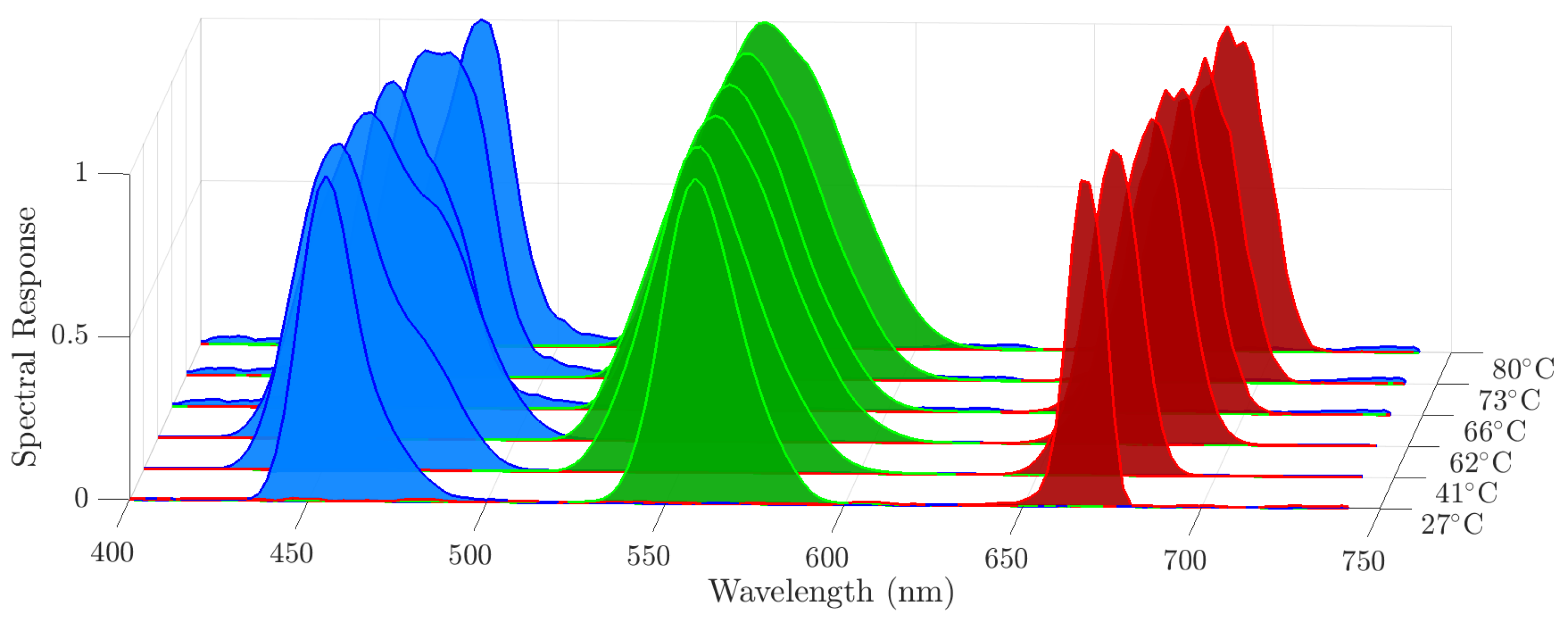
3.3. Emitted Spectrum versus Temperature
4. Channel Compensation in Optical Camera Communication

5. Methodology
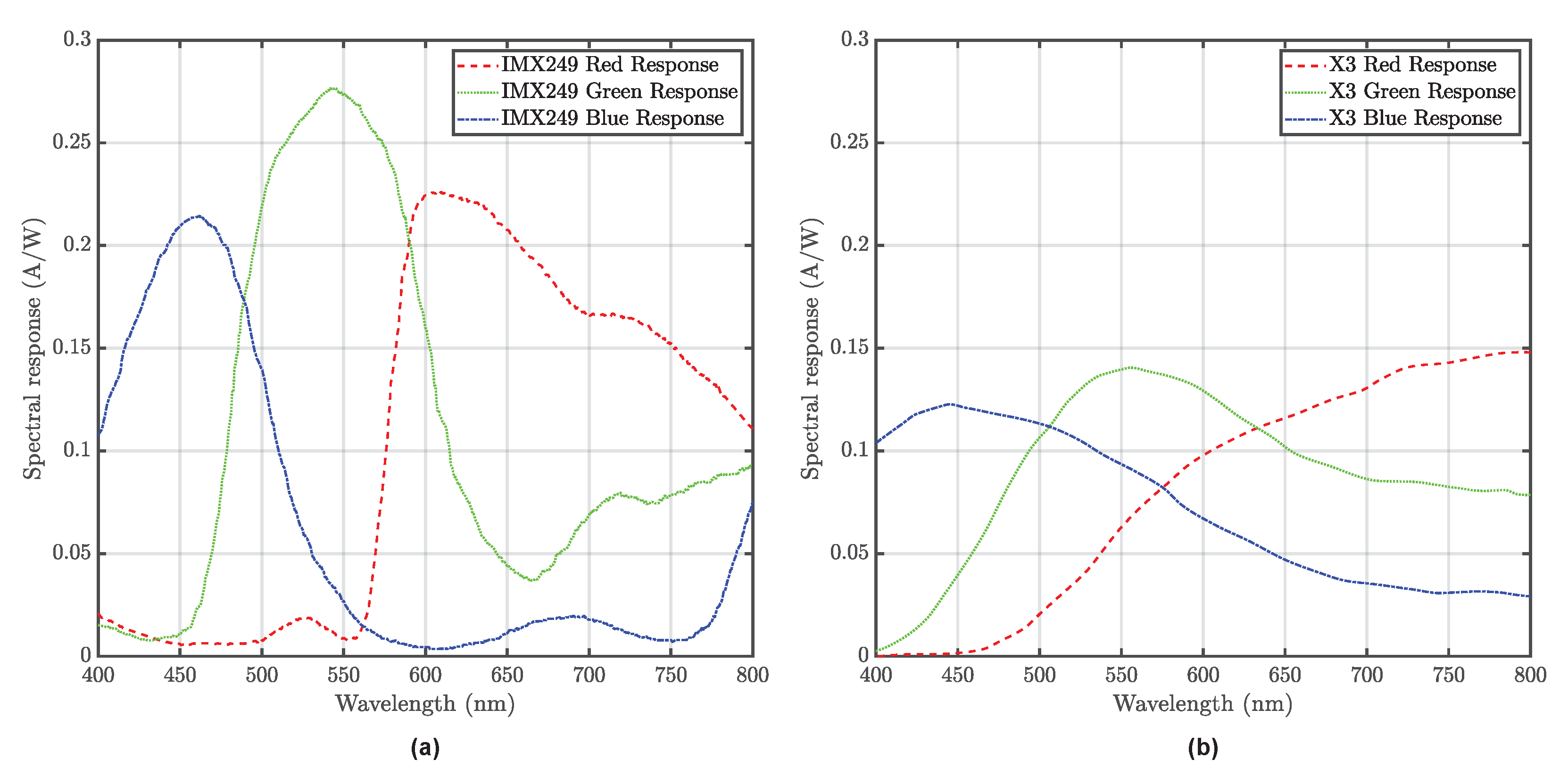
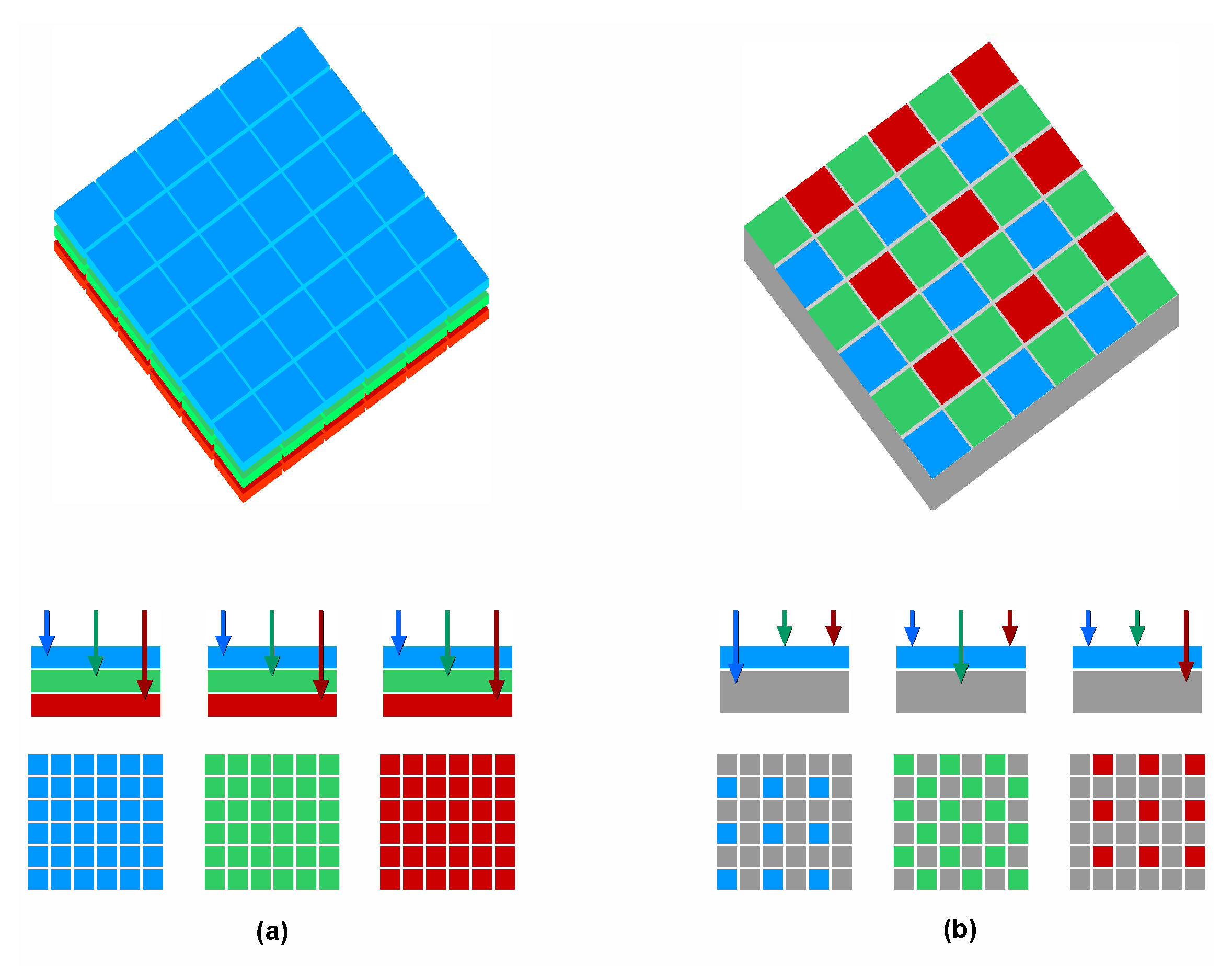
5.1. Experimental Setup
5.2. Description of the Experiment
6. Results
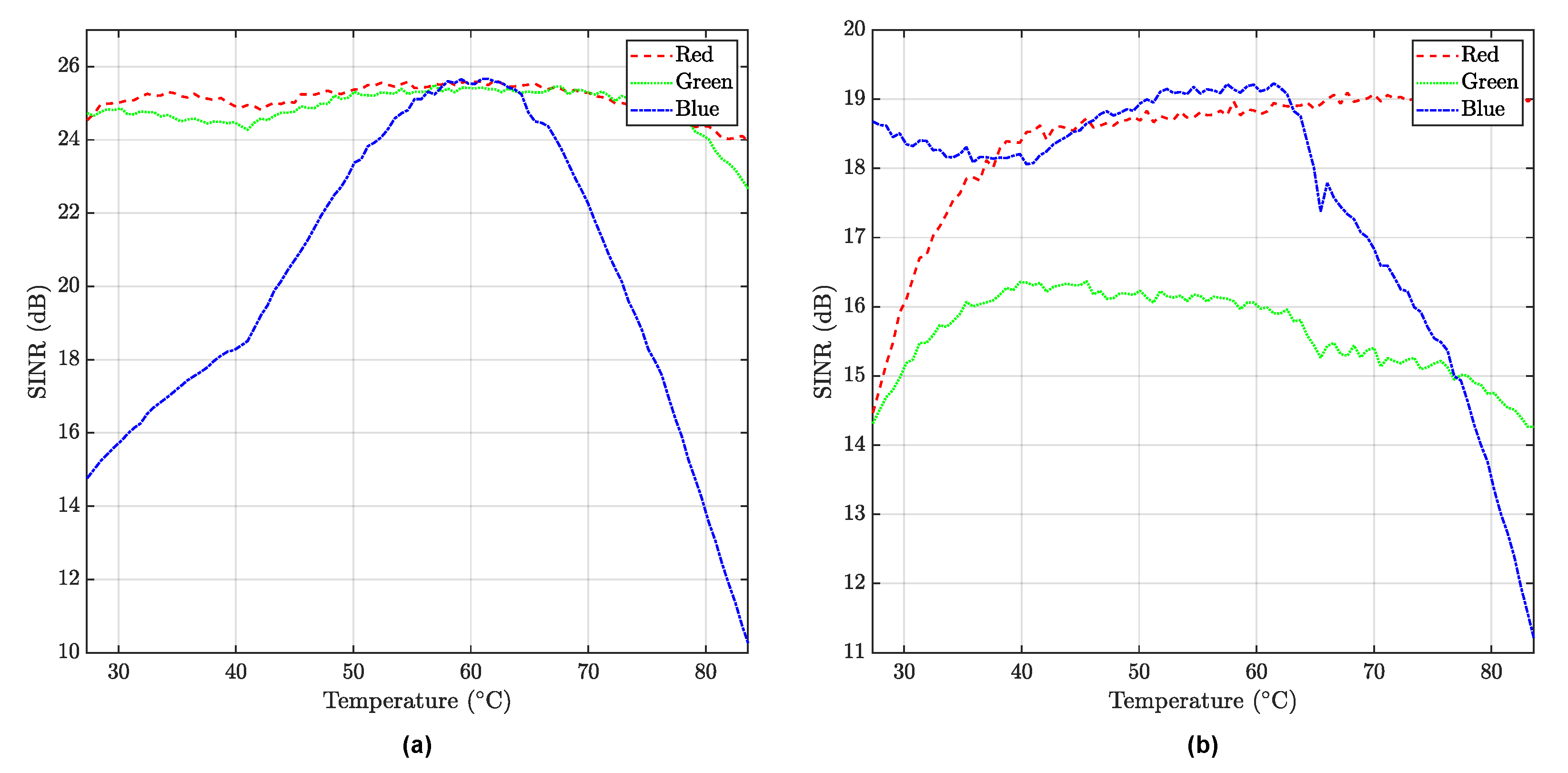
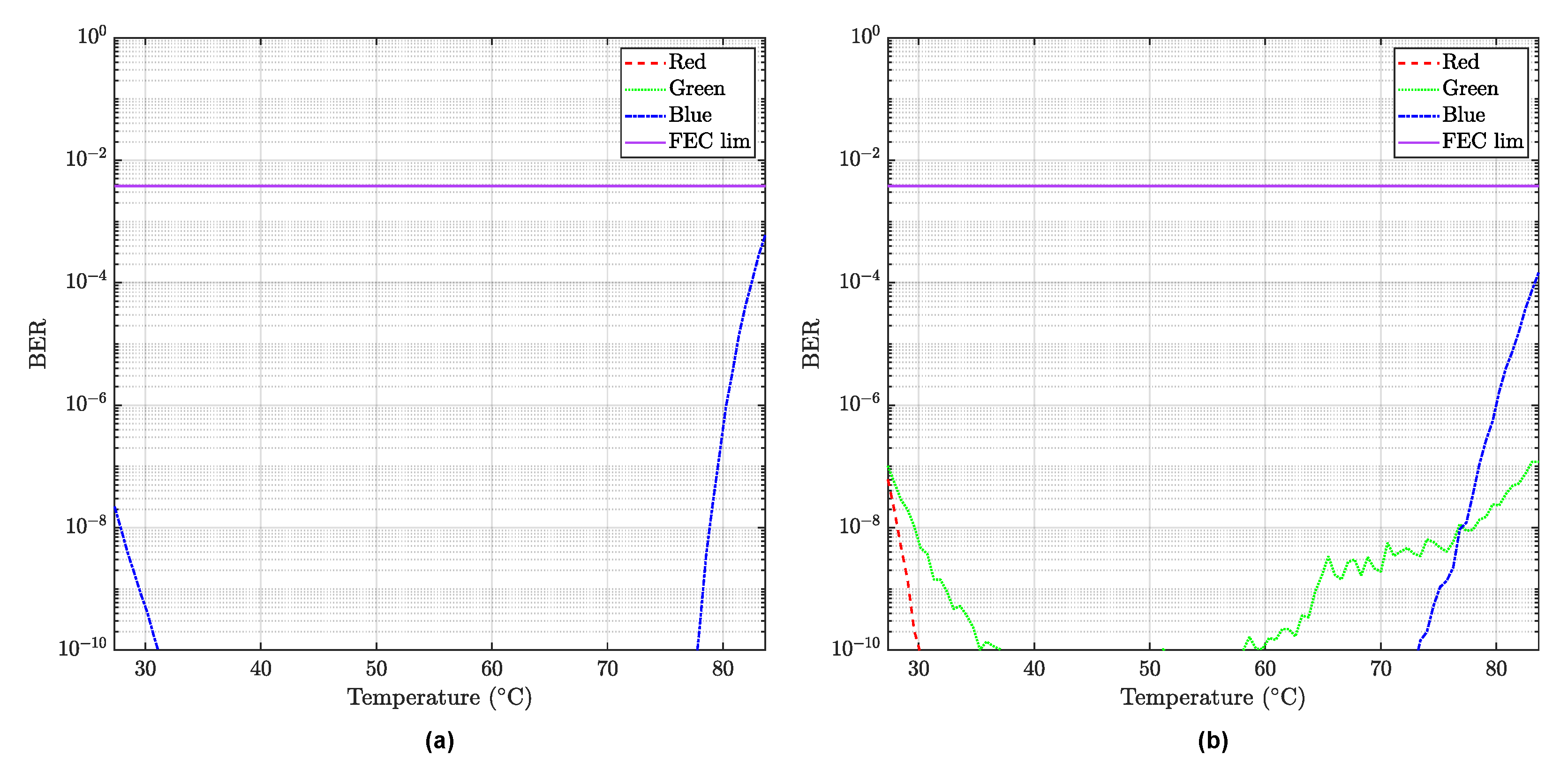
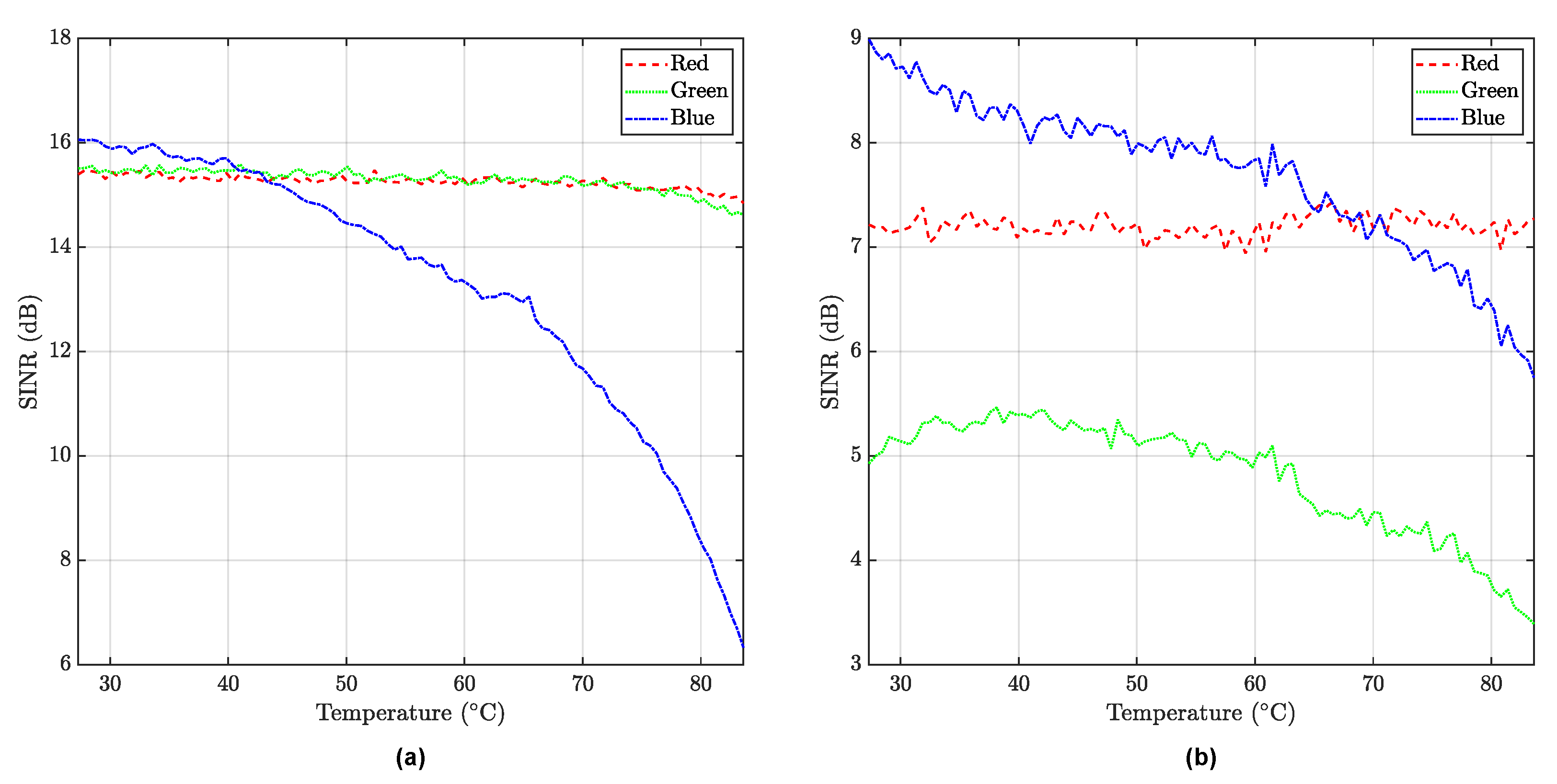
6.1. High SNR Case
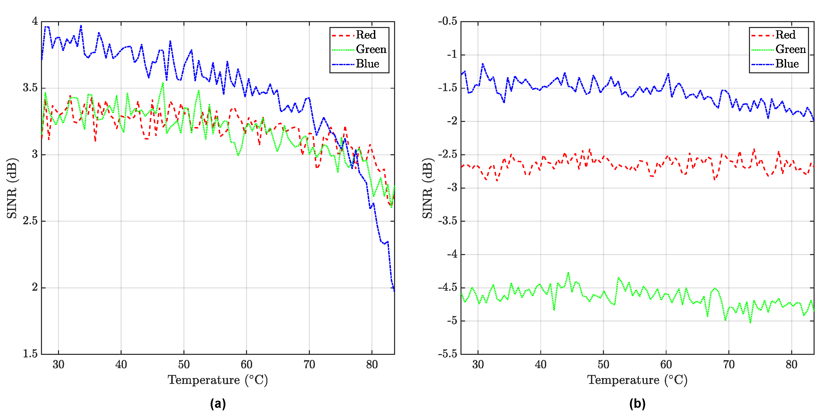
6.2. Medium SNR Case
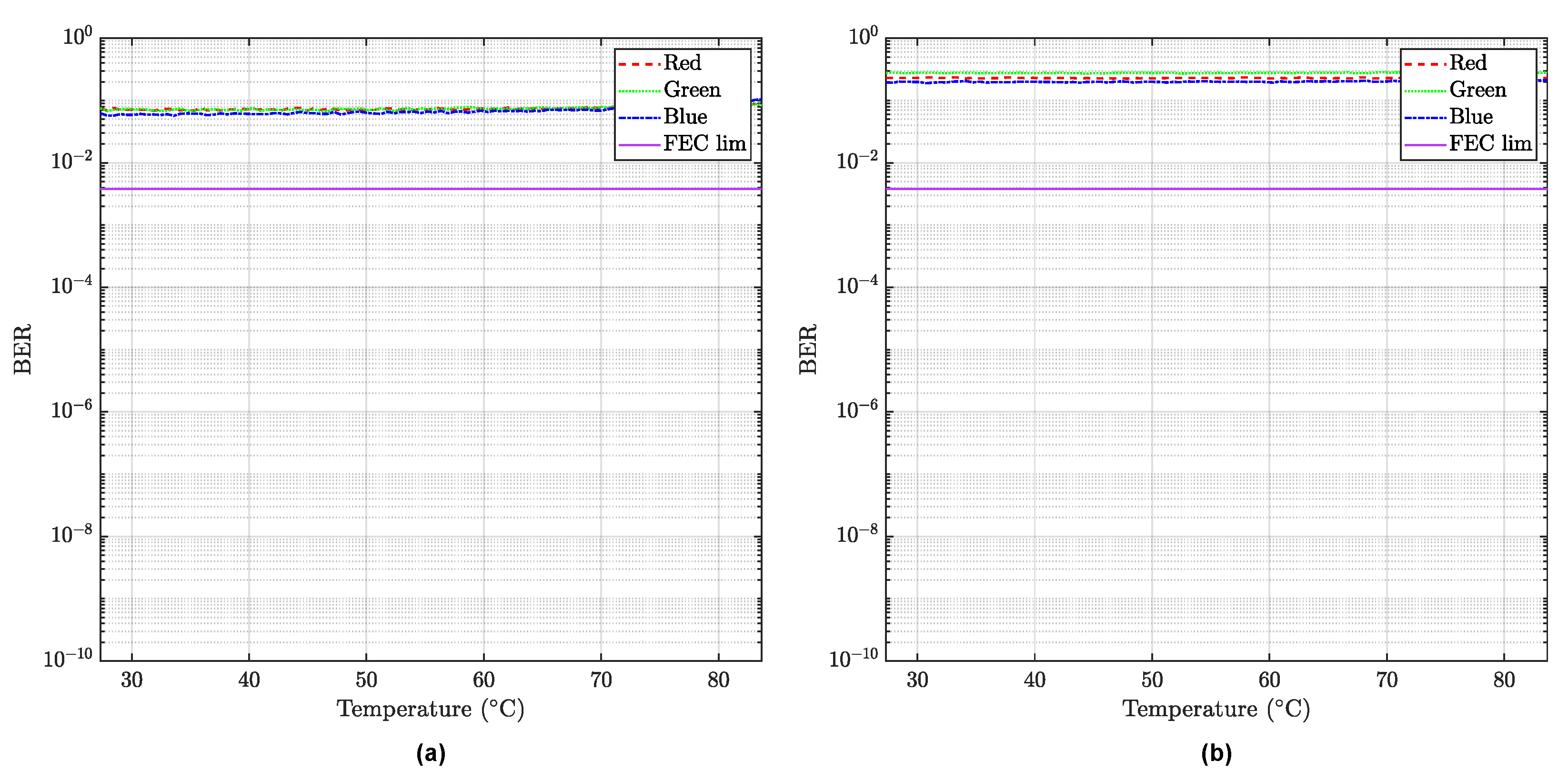
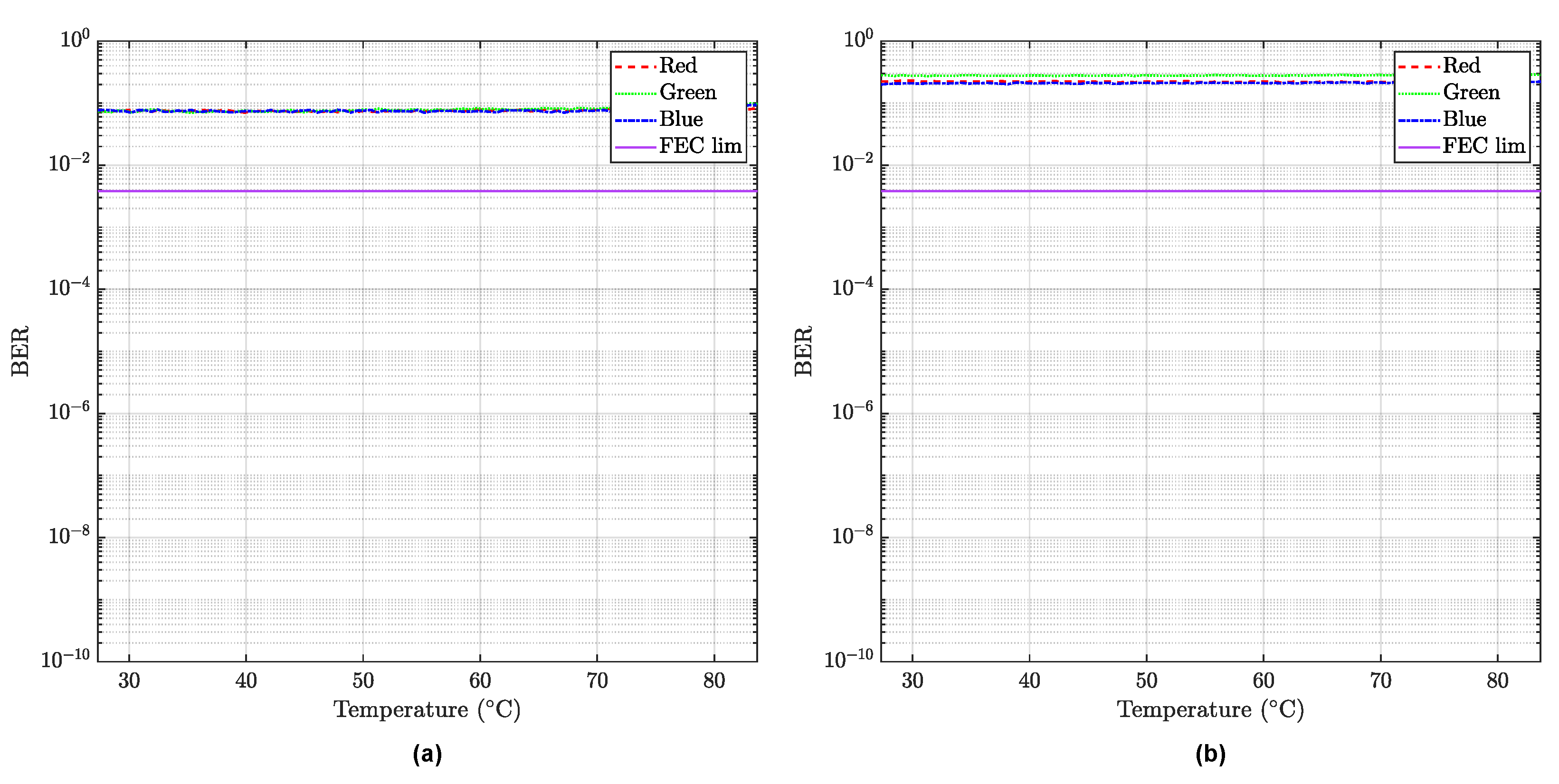
6.3. Low SNR Case
7. Conclusions
Author Contributions
Funding
Conflicts of Interest
References
- IEEE 802.15 Work Group. IEEE Standard for Local and Metropolitan Area Networks–Part 15.7: Short-Range Optical Wireless Communications; IEEE Std 802.15.7-2018 (Revision of IEEE Std 802.15.7-2011); IEEE: Piscataway, NJ, USA, 2019; pp. 1–407. [Google Scholar] [CrossRef]
- Bani Hassan, N.; Ghassemlooy, Z.; Zvanovec, S.; Biagi, M.; Vegni, A.M.; Zhang, M.; Luo, P. Non-Line-of-Sight MIMO Space-Time Division Multiplexing Visible Light Optical Camera Communications. J. Light. Technol. 2019, 37, 2409–2417. [Google Scholar] [CrossRef]
- Chavez-Burbano, P.; Guerra, V.; Rabadan, J.; Perez-Jimenez, R. Optical camera communication for smart cities. In Proceedings of the 2017 IEEE/CIC International Conference on Communications in China (ICCC Workshops), Qingdao, China, 22–24 October 2017; pp. 1–4. [Google Scholar]
- Do, T.; Yoo, M. A Multi-Feature LED Bit Detection Algorithm in Vehicular Optical Camera Communication. IEEE Access 2019, 7, 95797–95811. [Google Scholar] [CrossRef]
- Hasan, M.K.; Shahjalal, M.; Chowdhury, M.Z.; Jang, Y.M. Access Point Selection in Hybrid OCC/RF eHealth Architecture for Real-Time Remote Patient Monitoring. In Proceedings of the 2018 International Conference on Information and Communication Technology Convergence (ICTC), Jeju, Korea, 17–19 October 2018; pp. 716–719. [Google Scholar]
- Liu, X.; Wei, X.; Guo, L. DIMLOC: Enabling High-Precision Visible Light Localization Under Dimmable LEDs in Smart Buildings. IEEE Internet Things J. 2019, 6, 3912–3924. [Google Scholar] [CrossRef]
- Lin, X.; Zhang, L. Intelligent and Practical Deep Learning Aided Positioning Design for Visible Light Communication Receivers. IEEE Commun. Lett. 2020, 24, 577–580. [Google Scholar] [CrossRef]
- Chavez-Burbano, P.; Guerra, V.; Rabadan, J.; Rodríguez-Esparragón, D.; Perez-Jimenez, R. Experimental Characterization of Close-Emitter Interference in an Optical Camera Communication System. Sensors 2017, 17, 1561. [Google Scholar] [CrossRef] [PubMed]
- Liu, W.; Xu, Z. Some practical constraints and solutions for optical camera communication. Philos. Trans. R. Soc. A Math. Phys. Eng. Sci. 2020, 378. [Google Scholar] [CrossRef]
- Jurado-Verdu, C.; Matus, V.; Rabadan, J.; Guerra, V.; Perez-Jimenez, R. Correlation-based receiver for optical camera communications. Opt. Express 2019, 27, 19150–19155. [Google Scholar] [CrossRef]
- Jee, J.; Kwon, G.; Park, H. A Comparative Study on the Compensation Schemes for Transceiver I/Q Imbalances of Massive MIMO System. In Proceedings of the 2019 25th Asia-Pacific Conference on Communications (APCC), Ho Chi Minh City, Vietnam, 6–8 November 2019; pp. 292–296. [Google Scholar]
- Zhao, C.; Zhang, R.; Liu, B.; Fu, D.; Chen, H.; Li, M.; Xie, Z.; Xiu, X.; Gu, S.; Zheng, Y. The temperature dependence of optical properties of InGaN alloys. Sci. China Phys. Mech. Astron. 2012, 55, 396–399. [Google Scholar] [CrossRef]
- Park, J.; Lee, C.C. An electrical model with junction temperature for light-emitting diodes and the impact on conversion efficiency. IEEE Electron Device Lett. 2005, 26, 308–310. [Google Scholar] [CrossRef]
- Chen, H.; Lin, D.; Tan, S.; Hui, S.Y. Chromatic, Photometric and Thermal Modeling of LED Systems With Nonidentical LED Devices. IEEE Trans. Power Electron. 2014, 29, 6636–6647. [Google Scholar] [CrossRef]
- Almeida, P.S.; Bender, V.C.; Braga, H.A.C.; Dalla Costa, M.A.; Marchesan, T.B.; Alonso, J.M. Static and Dynamic Photoelectrothermal Modeling of LED Lamps Including Low-Frequency Current Ripple Effects. IEEE Trans. Power Electron. 2015, 30, 3841–3851. [Google Scholar] [CrossRef]
- Shen, X.; Chen, H.; Lin, J.; Li, Y.; Lin, H.; Chen, J.; Chen, C. Analysis and Modeling of Optical and Thermal Properties of Phosphor Converted White Light Emitting Diode. IEEE Access 2019, 7, 118679–118689. [Google Scholar] [CrossRef]
- Hui, S.Y.; Lee, A.T.L.; Tan, S. New Dynamic Photo-Electro-Thermal Modeling of Light-Emitting Diodes With Phosphor Coating as Light Converter Part I: Theory, Analysis, and Modeling. IEEE J. Emerg. Sel. Top. Power Electron. 2020, 8, 771–779. [Google Scholar] [CrossRef]
- Raypah, M.E.; Devarajan, M.; Sulaiman, F. Influence of injection current and ambient temperature on intensity and wavelength of low-power SMD LED. In Proceedings of the 2016 IEEE 37th International Electronics Manufacturing Technology (IEMT) & 18th Electronics Materials and Packaging (EMAP) Conference, George Town, Malaysia, 20–22 September 2016; Institute of Electrical and Electronics Engineers Inc.: Piscataway, NJ, USA, 2016. [Google Scholar] [CrossRef]
- Muthu, S.; Schuurmans, F.J.; Pashley, M.D. Red, green, and blue LED based white light generation: Issues and control. In Proceedings of the Conference Record of the 2002 IEEE Industry Applications Conference. 37th IAS Annual Meeting (Cat. No.02CH37344), Pittsburgh, PA, USA, 13–18 October 2002; Volume 1, pp. 327–333. [Google Scholar] [CrossRef]
- Spagnolo, G.S.; Papalillo, D.; Martocchia, A. LED Applications in Railway Signals: Wavelength and Intensity vs. Temperature Variation. J. Transp. Technol. 2012, 2, 78–83. [Google Scholar] [CrossRef][Green Version]
- Lu, B.; Wang, Y.; Hyun, B.R.; Kuo, H.C.; Liu, Z. Color Difference and Thermal Stability of Flexible Transparent InGaN/GaN Multiple Quantum Wells Mini-LED Arrays. IEEE Electron Device Lett. 2020, 41, 1040–1043. [Google Scholar] [CrossRef]
- Lee, Z.Y.; Devarajan, M. Simultaneous study of thermal and optical characteristics of light-emitting diode. In Proceedings of the 2012 10th IEEE International Conference on Semiconductor Electronics (ICSE), Kuala Lumpur, Malaysia, 19–21 September 2012; pp. 115–118. [Google Scholar] [CrossRef]
- Raypah, M.E.; Sodipo, B.K.; Devarajan, M.; Sulaiman, F. Estimation of Luminous Flux and Luminous Efficacy of Low-Power SMD LED as a Function of Injection Current and Ambient Temperature. IEEE Trans. Electron Devices 2016, 63, 2790–2795. [Google Scholar] [CrossRef]
- Chen, J.; Wan, N.; Li, J.; He, Z.; Wu, Y. A comparative study of properties and microstructures on thermal fatigue testing of a high-power LED. In Proceedings of the 2016 17th International Conference on Electronic Packaging Technology (ICEPT), Wuhan, China, 16–19 August 2016; Institute of Electrical and Electronics Engineers Inc.: Piscataway, NJ, USA, 2016; pp. 576–579. [Google Scholar] [CrossRef]
- Azhar, A.H.; Tran, T.; O’Brien, D. A Gigabit/s Indoor Wireless Transmission Using MIMO-OFDM Visible-Light Communications. IEEE Photonics Technol. Lett. 2013, 25, 171–174. [Google Scholar] [CrossRef]
- Zhong, W.; Chen, C.; Wu, D.; Ghassemlooy, Z. MIMO visible light communications system using imaging receiver with angle diversity detectors. In Proceedings of the 2016 15th International Conference on Optical Communications and Networks (ICOCN), Hangzhou, China, 24–27 September 2016; pp. 1–3. [Google Scholar] [CrossRef]
- Hong, Y.; Wu, T.; Chen, L. On the Performance of Adaptive MIMO-OFDM Indoor Visible Light Communications. IEEE Photonics Technol. Lett. 2016, 28, 907–910. [Google Scholar] [CrossRef]
- Ramirez-Aguilera, A.M.; Luna-Rivera, J.M.; Perez-Jimenez, R.; Rabadan-Borges, J.; Guerra, V.; Suarez-Rodriguez, C. Visible Light Communication Constraints in Practical Indoor Lighting Systems. In Proceedings of the European Wireless 2016; 22th European Wireless Conference, Oulu, Finland, 18–20 May 2016; pp. 1–5. [Google Scholar]
- Wei, L.; Zhang, H.; Song, J. Experimental Demonstration of a Cubic-Receiver-Based MIMO Visible Light Communication System. IEEE Photonics J. 2017, 9, 1–7. [Google Scholar] [CrossRef]
- Akande, K.O.; Popoola, W.O. MIMO Techniques for Carrierless Amplitude and Phase Modulation in Visible Light Communication. IEEE Commun. Lett. 2018, 22, 974–977. [Google Scholar] [CrossRef]
- Luo, P.; Zhang, M.; Ghassemlooy, Z.; Minh, H.L.; Tsai, H.M.; Tang, X.; Png, L.C.; Han, D. Experimental Demonstration of RGB LED-Based Optical Camera Communications. IEEE Photonics J. 2015, 7. [Google Scholar] [CrossRef]
- Anusree, A.; Jeyachitra, R.K. Performance analysis of a MIMO VLC (Visible Light Communication) using different equalizers. In Proceedings of the 2016 International Conference on Wireless Communications, Signal Processing and Networking (WiSPNET), Chennai, India, 23–25 March 2016; pp. 43–46. [Google Scholar] [CrossRef]
- Gao, Z.; Wang, Y.; Liu, X.; Zhou, F.; Wong, K. FFDNet-Based Channel Estimation for Massive MIMO Visible Light Communication Systems. IEEE Wirel. Commun. Lett. 2020, 9, 340–343. [Google Scholar] [CrossRef]
- Chen, H.W.; Wen, S.S.; Wang, X.L.; Liang, M.Z.; Li, M.Y.; Li, Q.C.; Liu, Y. Color-Shift Keying for Optical Camera Communication Using a Rolling Shutter Mode. IEEE Photonics J. 2019, 11. [Google Scholar] [CrossRef]
- Nguyen, T.; Thieu, M.D.; Jang, Y.M. 2D-OFDM for Optical Camera Communication: Principle and Implementation. IEEE Access 2019, 7, 29405–29424. [Google Scholar] [CrossRef]
- Rush, A.; Hubel, P. X3 Sensor Characteristics. J. Soc. Photogr. Sci. Technol. Jpn. 2003, 66, 57–60. [Google Scholar]
- Varshni, Y.P. Temperature dependence of the energy gap in semiconductors. Physica 1967, 34, 149–154. [Google Scholar] [CrossRef]
- Foschini, G.; Gans, M. On Limits of Wireless Communications in a Fading Environment when Using Multiple Antennas. Wirel. Pers. Commun. 1998, 6, 311–335. [Google Scholar] [CrossRef]
- Lin, D.L.; Wang, C.C.; Wei, C.L. Quantified temperature effect in a CMOS image sensor. IEEE Trans. Electron. Devices 2010, 57, 422–428. [Google Scholar] [CrossRef]
- Leven, A.; Vacondio, F.; Schmalen, L.; ten Brink, S.; Idler, W. Estimation of Soft FEC Performance in Optical Transmission Experiments. IEEE Photonics Technol. Lett. 2011, 23, 1547–1549. [Google Scholar] [CrossRef]


| Parameter | Value |
|---|---|
| Current source | Yokogawa GS820 |
| Spectrometer | Spectral Products SM442 |
| Integrating sphere | Gigahertz 32 cm |
| Thermal camera | FLIR A640 |
| CMOS sensors | Sony IMX249 and Foveon X3 |
| RGB LED under test | Kingbright L-154A4SUREQBFZGEW |
| Temperature range | 27 °C to 80 °C |
| Driving current | 10 mA to 150 mA |
| Red peak wavelength | 676 nm @ 10 mA |
| Green peak wavelength | 563 nm @ 10 mA |
| Blue peak wavelength | 460 nm @ 10 mA |
| Input SNR | 30 dB, 20 dB, 10 dB |
| Spectrometer’s integration time | 25 ms |
Publisher’s Note: MDPI stays neutral with regard to jurisdictional claims in published maps and institutional affiliations. |
© 2021 by the authors. Licensee MDPI, Basel, Switzerland. This article is an open access article distributed under the terms and conditions of the Creative Commons Attribution (CC BY) license (http://creativecommons.org/licenses/by/4.0/).
Share and Cite
Moreno, D.; Rufo, J.; Guerra, V.; Rabadan, J.; Perez-Jimenez, R. Effect of Temperature on Channel Compensation in Optical Camera Communication. Electronics 2021, 10, 262. https://doi.org/10.3390/electronics10030262
Moreno D, Rufo J, Guerra V, Rabadan J, Perez-Jimenez R. Effect of Temperature on Channel Compensation in Optical Camera Communication. Electronics. 2021; 10(3):262. https://doi.org/10.3390/electronics10030262
Chicago/Turabian StyleMoreno, Daniel, Julio Rufo, Victor Guerra, Jose Rabadan, and Rafael Perez-Jimenez. 2021. "Effect of Temperature on Channel Compensation in Optical Camera Communication" Electronics 10, no. 3: 262. https://doi.org/10.3390/electronics10030262
APA StyleMoreno, D., Rufo, J., Guerra, V., Rabadan, J., & Perez-Jimenez, R. (2021). Effect of Temperature on Channel Compensation in Optical Camera Communication. Electronics, 10(3), 262. https://doi.org/10.3390/electronics10030262