Article

Design of A Ka-Band 3D-Printed Dual-Polarization Magnetoelectric Dipole Antenna Array with Low Sidelobe

Beijing Key Laboratory of Millimeter Wave and Terahertz Techniques, School of Integrated Circuits and Electronics, Beijing Institute of Technology, Beijing 100081, China
*
Author to whom correspondence should be addressed.
Electronics 2021, 10(23), 2969; https://doi.org/10.3390/electronics10232969
Submission received: 6 November 2021 / Revised: 22 November 2021 / Accepted: 23 November 2021 / Published: 29 November 2021
(This article belongs to the Section Microwave and Wireless Communications)

Abstract

:
A Ka-band dual-polarization magnetoelectric (ME) dipole antenna array based on three-dimensional (3D)-printed technology with low sidelobe level (SLL) is proposed in this paper. The metal posts and cross-slots are explored to build a novel subarray with 2 × 2-unit ME-dipoles as the basic element. Creatively, a square waveguide to cross-slots transition with a pyramid horn cavity structure is investigated to feed the ME-dipole subarray. Furthermore, two types of power-tapering corporate-feed networks with laminated structures are used to design an 8 × 8-unit low-SLL array. The fabricated array has a relative bandwidth (VSWR < 2) of 14.3% and 17.1%, with a realized gain higher than 25.8 dBi and 26.1 dBi for the H-pol. and V-pol., respectively. The maximum radiation efficiency for both arrays is 73.2%. The measured first sidelobe levels are less than –17.5 dB for both polarizations. With competitive performance and low fabrication cost, the proposed dual-polarization ME-dipole antenna array would be valuable for polarization-agile radar and communication systems.

Graphical Abstract

1. Introduction

A dual-polarization antenna with wideband, high-gain and low-sidelobe characteristics is required for mm-wave radars to achieve high resolution, high detection accuracy and strong anti-interference ability [1,2]. Various dual-polarization antenna arrays based on dielectric transmission lines have been reported, such as aperture-coupled microstrip patch arrays [3,4], slot-coupling series-feed microstrip patches [5] and substrate-integrated waveguide (SIW) feed antenna arrays [6,7,8]. These antennas feature high isolation, low profile and low cost, but their operation bandwidth is narrow. ME-dipole arrays have excellent impedance bandwidth and symmetric radiation patterns [9]. The strip-line feed dual-polarization ME-dipole array based on LTCC technology in [10] and the SIW feed array based on multilayer PCB technology in [11] both have wideband and low-profile features. However, the substrate loss of the above arrays can no longer be ignored with the increase in the array dimension in the mm-wave band.
Antenna arrays based on air-filled waveguides have lower transmission loss and higher radiation efficiency. The dual-polarization slotted wave-guide array in [12,13,14] has a low-sidelobe design with high polarization isolation, but the series feed limits its working bandwidth. The full corporate-feed waveguide slot array with dual-polarization in [15,16] has wideband and high-gain features, but the diffusion bonding process brings high fabrication cost. By using gap waveguide technology without any bonding process for full corporate-feed slot arrays [17,18], the difficulty and cost of fabrication can be reduced while achieving high gain. However, the bandwidth is still limited, as the basic array unit is based on a narrowband resonant structure. Recently, 3D-printing technology has been widely used for mm-wave antenna arrays [19,20,21,22], which offers a new method for the design and fabrication of antennas with complex structures that cannot be manufactured by traditional methods. A new form of ME-dipole element combined with a waveguide feed network was proposed to achieve wideband and high-efficiency radiation characteristics [19]. Furthermore, special structures such as a roof-shaped cavity and a waveguide with arc-shaped short walls were proposed for 3D-printing technology, which can reduce the fabrication time and cost [20]. However, they are limited to single-polarization applications. In [21], stepped cavities with laminated E-plane rectangular waveguide (ERWG) feed networks were proposed to realize a dual-circular-polarization antenna array at 13 GHz. The array has wideband and lightweight characteristics, but its isolation and cross-polarization discriminations (XPD) are not high. In [22], a dual-polarization ME-dipole unit with a differential feeding cavity structure was proposed, which realizes an impedance-matching bandwidth of 30% with a high gain of 28.5 dBi. Nevertheless, an extra WG divider is needed to realize the differential feeding, which increases the complexity and insertion loss of the feed network.
In this paper, an approach to realize a dual-polarization ME-dipole array with 3D-printed technology is proposed. The metal posts and cross-slots are explored to build the ME-dipole. Moreover, a new transition structure from a square waveguide to cross-slots is invented to excite the ME-dipole. A 2 × 2-unit subarray with a pyramid horn cavity is designed to pursue wideband and high-isolation properties. Based on a 2 × 2-unit subarray, an 8 × 8-unit array is meticulously designed and fabricated by direct metal laser sintering technology. Two power-tapering corporate-feed networks are employed to achieve low SLL of the dual-polarization array. The measured results illustrate the fabricated array has wideband (14.3% and 17.1% with VSWR < 2), low-sidelobe (below –17.5 dB), high-isolation (≥30 dB) and high cross-polarization discriminations (≥32 dB).

2. The Dual-Polarization 2 × 2-Unit ME-Dipole Subarray

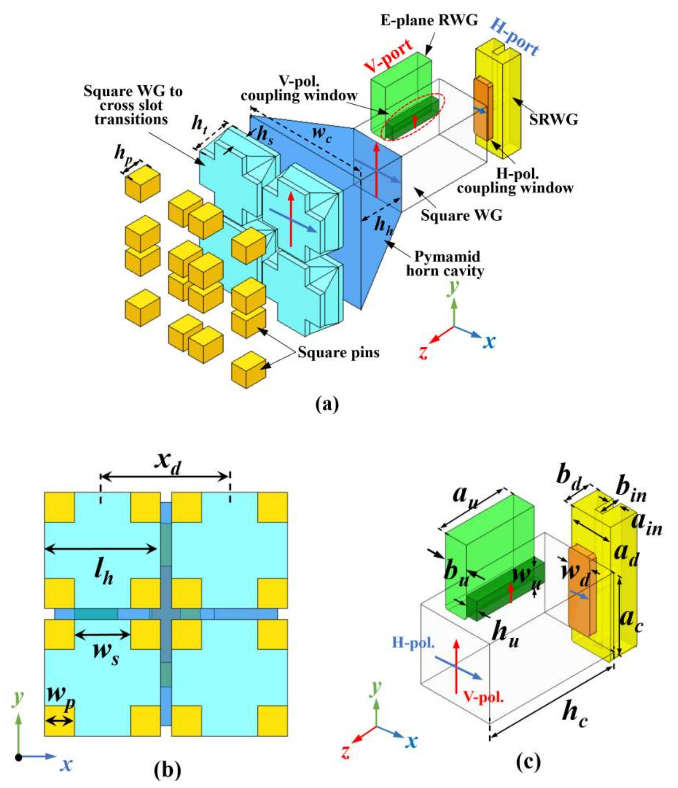
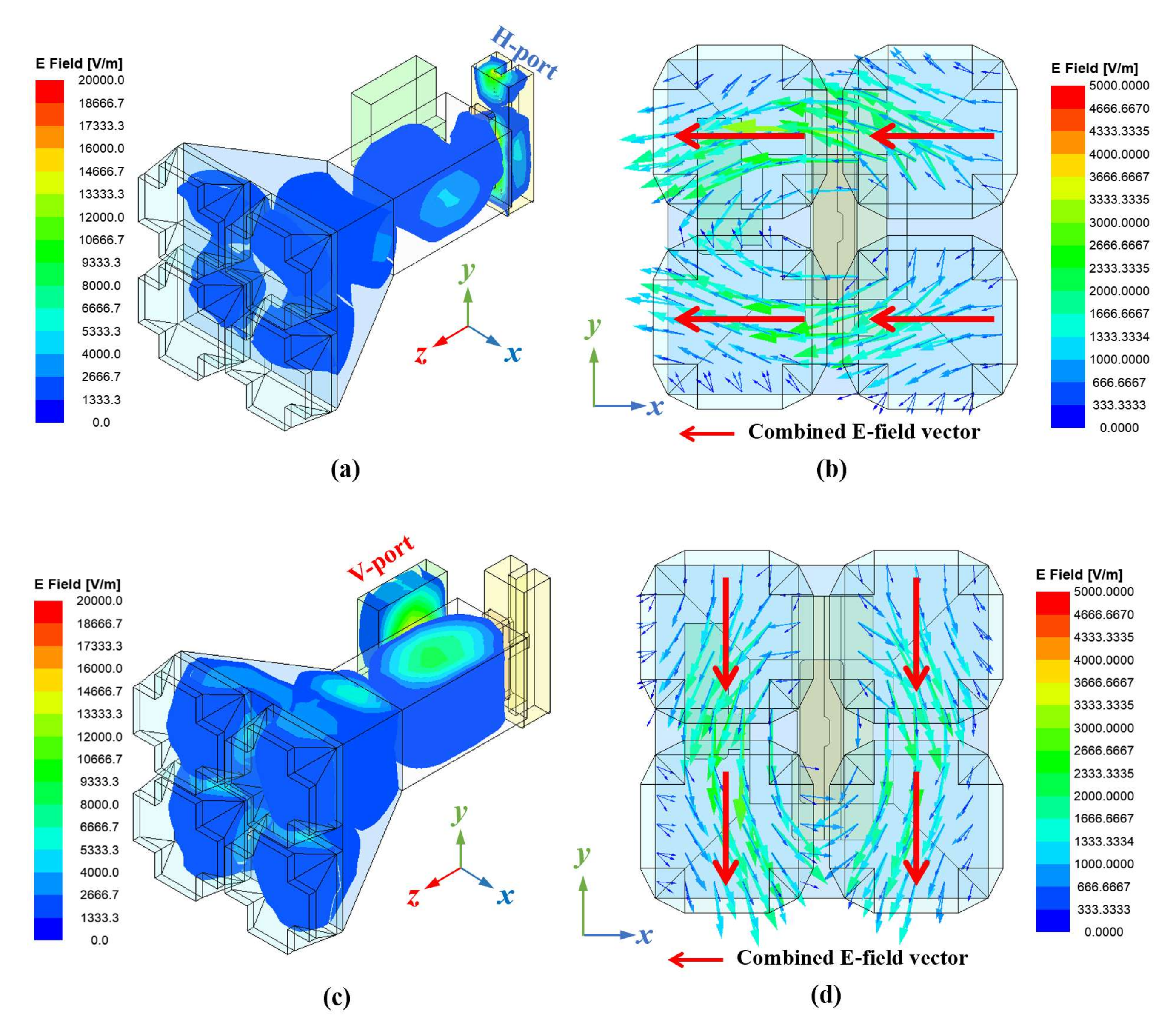
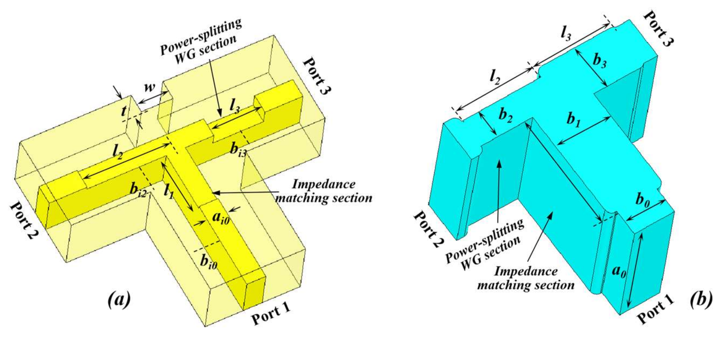
2.1. Configuration and Operation Mechanism

Figure 1a shows the configuration of the proposed dual-polarization antenna element with a four-layer structure. On the top layer, four short-end patches, which are excited by the cross-slots on the second layer, are evenly distributed at the corners. On the third layer, a novel gradient transition structure is proposed to feed the cross-slots through a square WG. This structure is easily realized by 3D-printing technology. By comparison with the cavity-excited cross-slots in [15,22], the complexity of the proposed antenna is reduced. The fourth layer is the feeding square WG, which can easily connect with an orthomode transducer (OMT) and achieve the function of dual-polarization radiation. Furthermore, an improved dual-polarization unit is also studied, as shown in Figure 1b. The metal posts are used to replace the short-end patches. This simplified structure can effectively reduce the fabrication difficulty, especially for large-scale arrays.
The electric magnetic simulation software ANSYS Electronics Desktop was utilized to reveal the operation principle of the proposed dual-polarization ME-dipole. Figure 2 displays the electric field and surface current distributions of the ME-dipole single unit. At t = 0, the surface current is strong at the side surfaces of the posts in Figure 2a. The surface current and E-field are weak at the top surface of the posts and the aperture between the posts in Figure 2c. It signifies that the equivalent magnetic dipole in the x-direction is excited. At t = T/4, the sinusoidal distribution of the surface current can be observed at the top surface of the posts in Figure 2b. The E-field is also strong over the aperture between the posts in Figure 2d, which indicates that the metal posts consist of equivalent electric dipoles in the y-direction. The electric dipole and magnetic dipole are excited alternatively, which forms the EM-dipole unit. The same distribution will appear on the orthogonal planes when another orthogonally polarized port is excited.
Based on the proposed dual-polarization ME-dipole unit, the array layout of the design was carried out. In order to further simplify the structure of the total array, a horn cavity was employed to excite the 2 × 2-unit ME-dipoles, which formed a subarray. The geometry of the dual-polarization subarray is displayed in Figure 3. It can be divided into two parts: the radiation part and the feeding part. The four ME-dipoles with metal posts and cross-slots constitute the radiation part. The first layer of the feeding part comprises four square WGs to cross-slots transition structures. The pyramid horn cavity is laid on the second layer. It can not only reduce the complexity of the feed network for the total array but can also decrease the feed loss of the total array and expand the bandwidth of the array. In addition, by comparison with the step cavities in [23], the pyramid horn cavity is more conducive to the 3D-printing technology. The orthomode transducer composed of vertical square WGs and two orthogonal coupling windows is utilized to feed the radiation part with high isolation. The E-plane RWG and single-ridge WG (SRWG) are employed as two feeding transmission lines.
Figure 4a,b shows the distribution of electric fields in the subarray when fed by the H-pol. port. The quasi-TE10 mode in the SRWG is transmitted into the square WG through the H-pol. coupling window, and the TE01 mode is excited in the square WG. The E-field direction of the TE01 mode in the square WG is parallel with the V-pol. coupling window. The EM-wave from the H-port is cut off by the V-pol. coupling window. The two orthogonal coupling windows structure can attain high isolation between the two orthogonal polarization ports. The directions of the combined E-field over the four cross-slots’ apertures are along the x-direction, which form the H-pol. radiation. Figure 4c,b gives the distributions of electric fields in the subarray when fed by the V-pol. Port. The TE10 mode is excited in the square WG, and the direction of the combined E-field over the four cross-slots’ apertures is along the y-direction, which forms the V-pol. radiation.

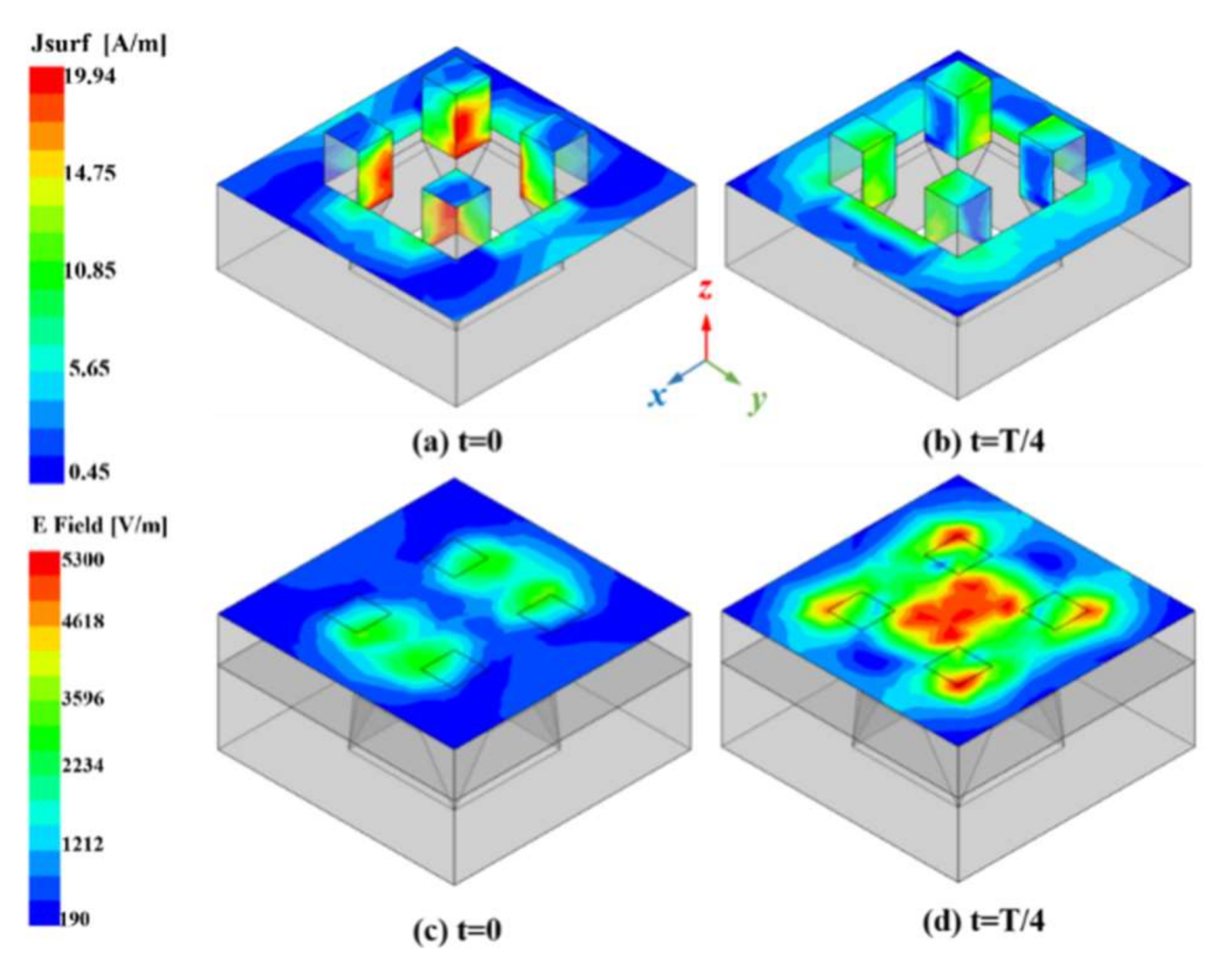
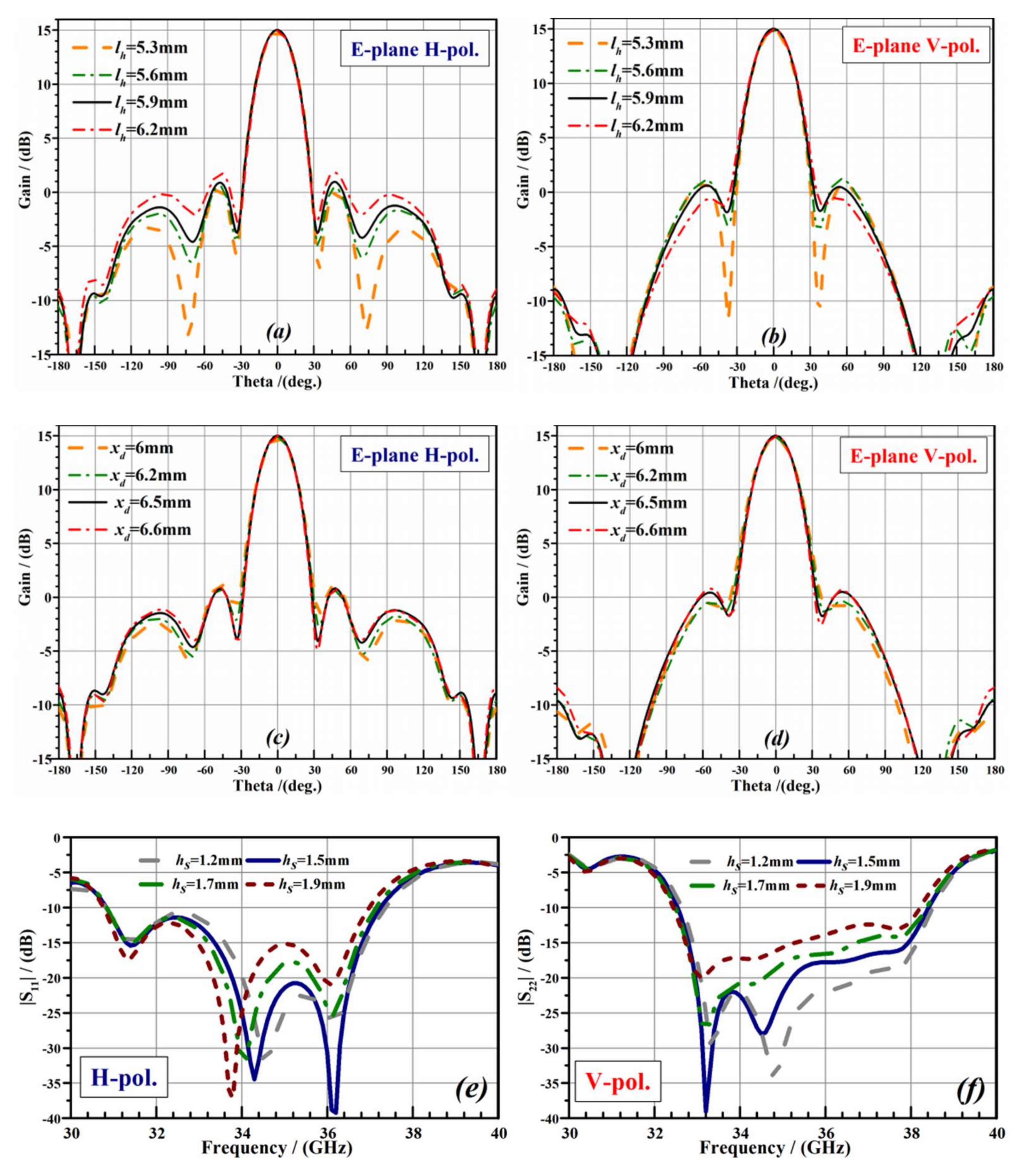
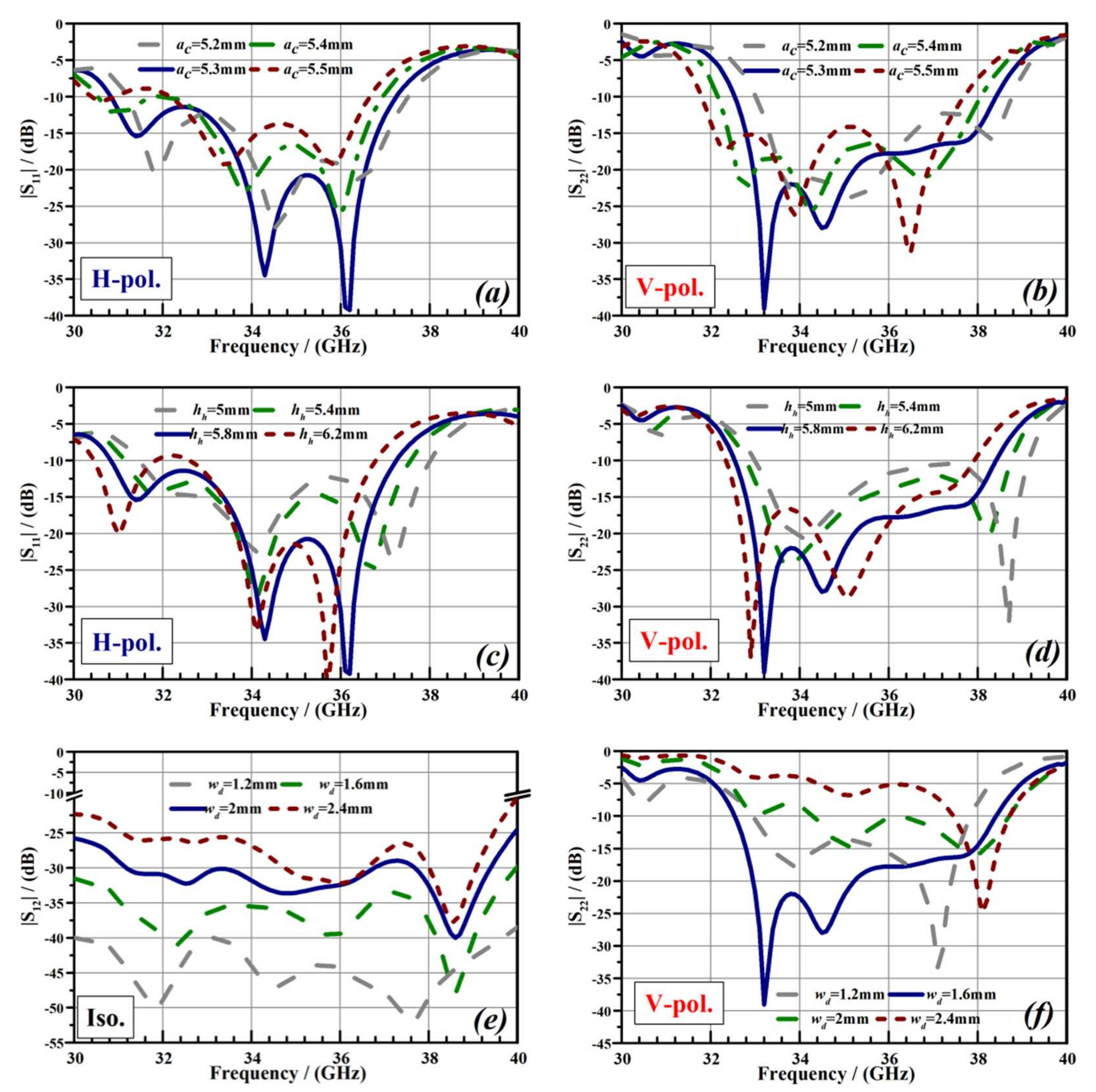
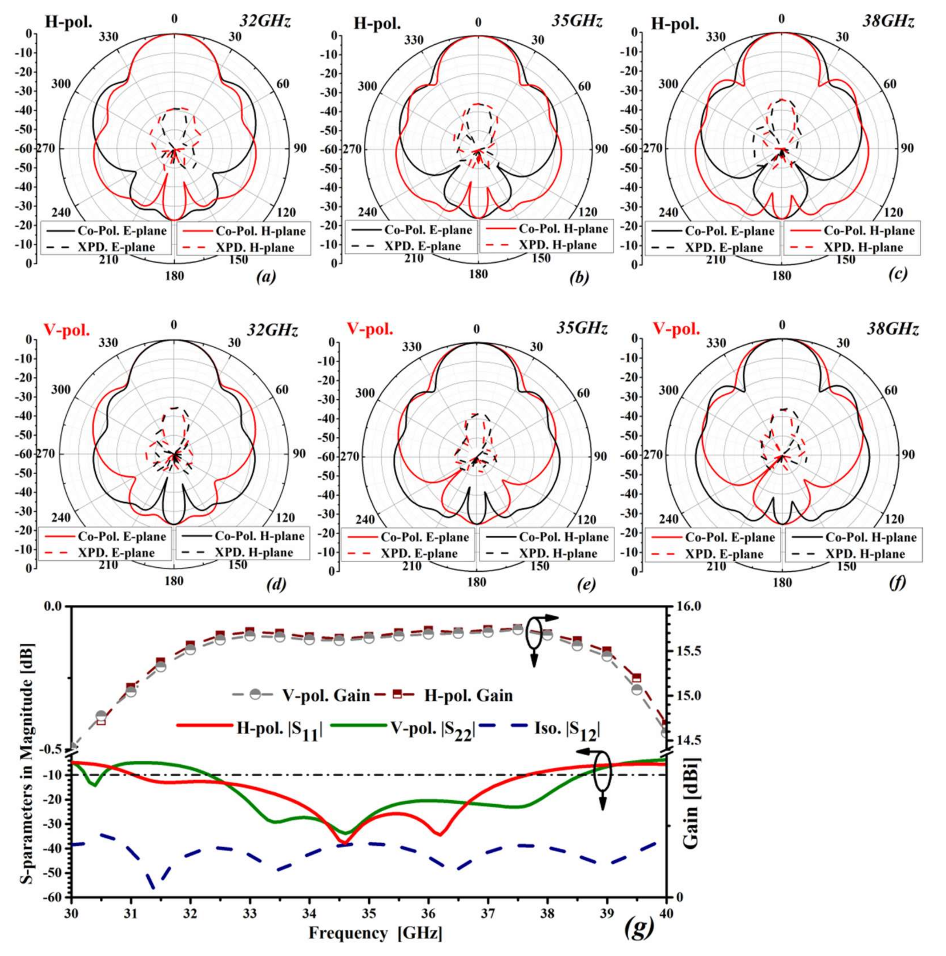
2.2. Performance and Parameter Analysis of the Subarray

The working mechanism of the proposed dual-polarization ME-dipole unit is discussed in the previous section. Some key parameters are studied to guide the design of the dual-polarization antenna. According to the working mechanism of the ME-dipoles, the height of the posts hp, the length (lh) of the cross-slots and the width length ratio (ws /lh) are set to 0.25, 0.4 and 0.6, respectively. The distance between the adjacent ME-dipoles (xd) is set to 0.76 λ0. The height of the cross-slots is set to 0.1 λ0. The simulated gains of the subarray with different lh and xd values for H- and V-polarizations are shown in Figure 5a–d. It shows that the gains of the two polarization units increase with increasing lh. However, the sidelobe level also rises with increasing lh. Therefore, in consideration of the high gain and low sidelobe, the value of lh is set to 5.9 mm. Similarly, the subarray gain increases with increasing xd and reaches the highest when xd is equal to 6.5 mm. By tuning the two key parameters, a proper gain can be achieved. Additionally, the height of the transition (hs) affects the impedance-matching performance of the subarray notably. The reflection coefficients of the two ports for different hs values are shown in Figure 5e,f. The impedance-matching bandwidth of the H-pol. port increases when hs becomes smaller. However, the reflection coefficient of the V-pol. port will worsen when hs becomes smaller. Finally, the value of hs is set to 1.5 mm.
The width of the pyramid horn cavity, which is determined by the distance and the length of the cross-slots, is set to 11.8 mm. The H-pol. And V-pol. Coupling windows have the width of the square WG (ac) and the width of the ERWG (au), separately. The matching performance of the two feeding WGs is determined by the width of the square WG and the height of the pyramid horn cavity. The reflection coefficients of the two ports with different ac and hh values are shown in Figure 6a–d. It shows that the influence trend of those parameters on the two ports is opposite, so there is an optimal solution for both parameters. In addition, the isolation between the two orthogonal polarization ports with different wd values is shown in Figure 6e. It shows that the isolation rises with decreasing wd. Finally, the value of wd is set to 1.6 mm in consideration of the best impedance bandwidth performance, which is shown in Figure 6f. Following the above design guidelines, better radiation and feeding performance of the dual-polarization ME-dipole subarray can be achieved.
The optimized dimensions of the subarray are listed in Table 1. Figure 7 shows the simulated performances of the proposed dual-polarization 2 × 2-unit ME-dipole subarray. The simulated reflection coefficients less than –10 dB bandwidth for the H-pol. and V-pol. subarrays are 18% (31.1–37.6 GHz) and 17% (32.4–38.4 GHz), respectively. Isolation between the two ports is higher than 35 dB. The gains for both H-pol. and V-pol. are varied from 15.2 dBi to 15.8 dBi over the operation band. The stable radiation patterns can be observed for both subarrays from 32 GHz to 38 GHz. The backlobe level is less than –23 dB for the two subarrays. The simulated results exhibit that the proposed dual-polarization ME-dipole subarray has wide impedance-matching bandwidth with good radiation performance.

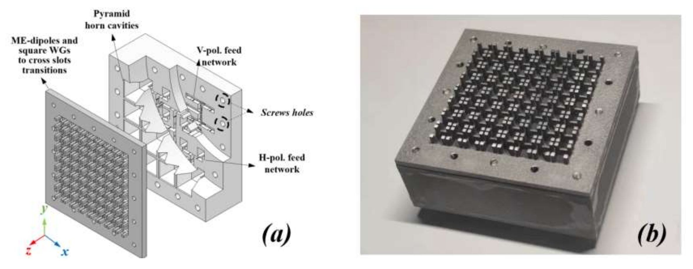
3. Design of the Low-Sidelobe 8 × 8-Unit Dual-Polarization ME-Dipole Array

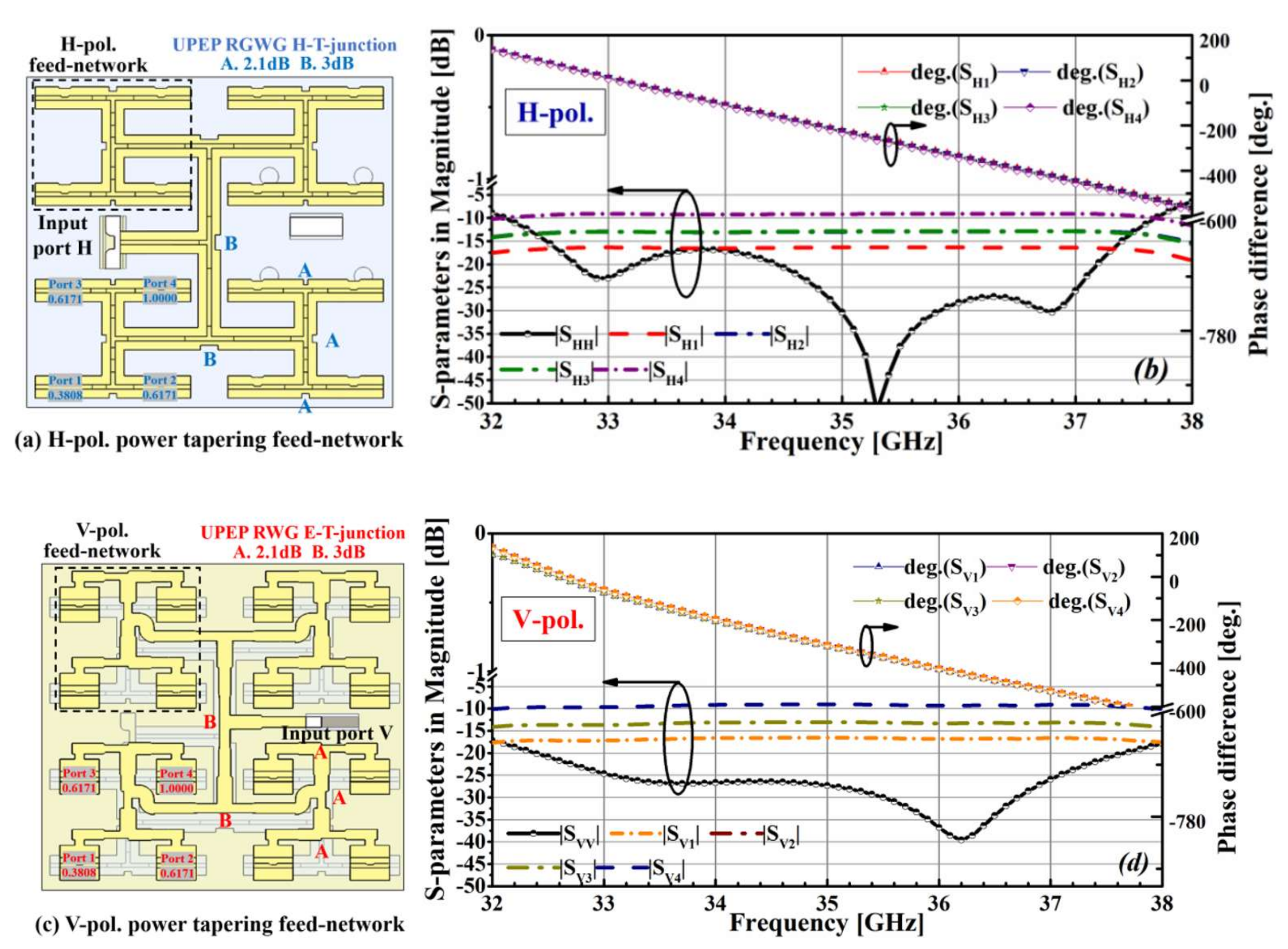
3.1. Antenna Geometry and Low-Sidelobe Design

Based on the dual-polarization 2 × 2-unit ME-dipole subarray, an 8 × 8-unit dual-polarization antenna array was designed. The spacing between the adjacent subarrays was 13 mm (1.52 λ0) in both the x-direction and y-direction. In order to realize the low-sidelobe design of the two arrays, two kinds of 1-to-16 power-tapering corporate-feed networks based on E-plane WG and SRWG were designed and simulated, respectively.
The unequal-power but equal-phase (UPEP) E-plane WG divider and the UPEP SRWG were employed to construct the feed networks. Figure 8a,b shows the geometry of the UPEP SRWG and UPEP E-plane WG divider, respectively. Three WGs sections were introduced into the two UPEP dividers as the impedance transformers. The power-splitting ratio between the output ports can be tuned by adjusting the parameters: narrow wall width (b2 and b3), ridge height (bi2 and bi3) and length of the two WG sections (l2 and l3). Based on this tuning method, the phase difference between the output ports can be controlled within a small range.
Figure 9a,c shows the geometry of the two power-tapering feed networks, respectively. The 20 dB Taylor synthesis with the unit spacing of 1.52 λ0 was utilized to calculate the normalized amplitude coefficient of each output port, as shown in Figure 9a,c. The simulated performances of the two feed networks are shown in Figure 8b,d. The phase and amplitude differences among all the output ports are within ±10° and ±0.5 dB for both feed networks. The reflection coefficient of the two input ports is both less than –15 dB, covering the bandwidth range of 32.5 GHz to 37.5 GHz.

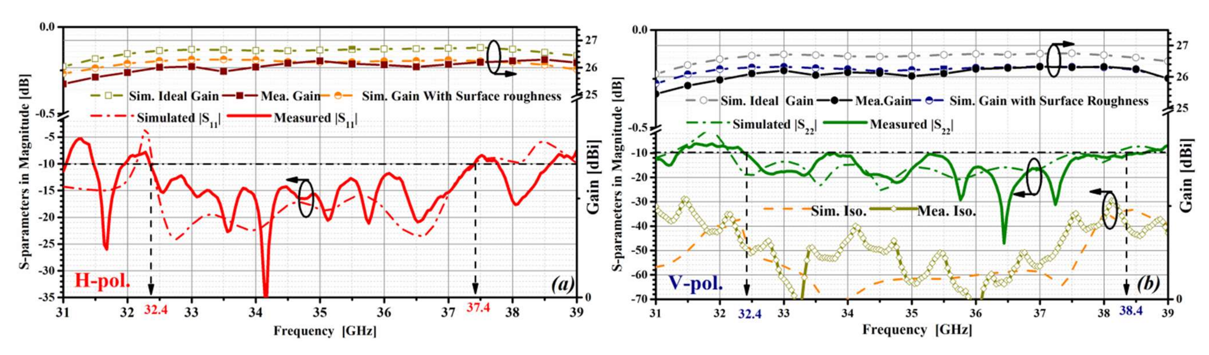
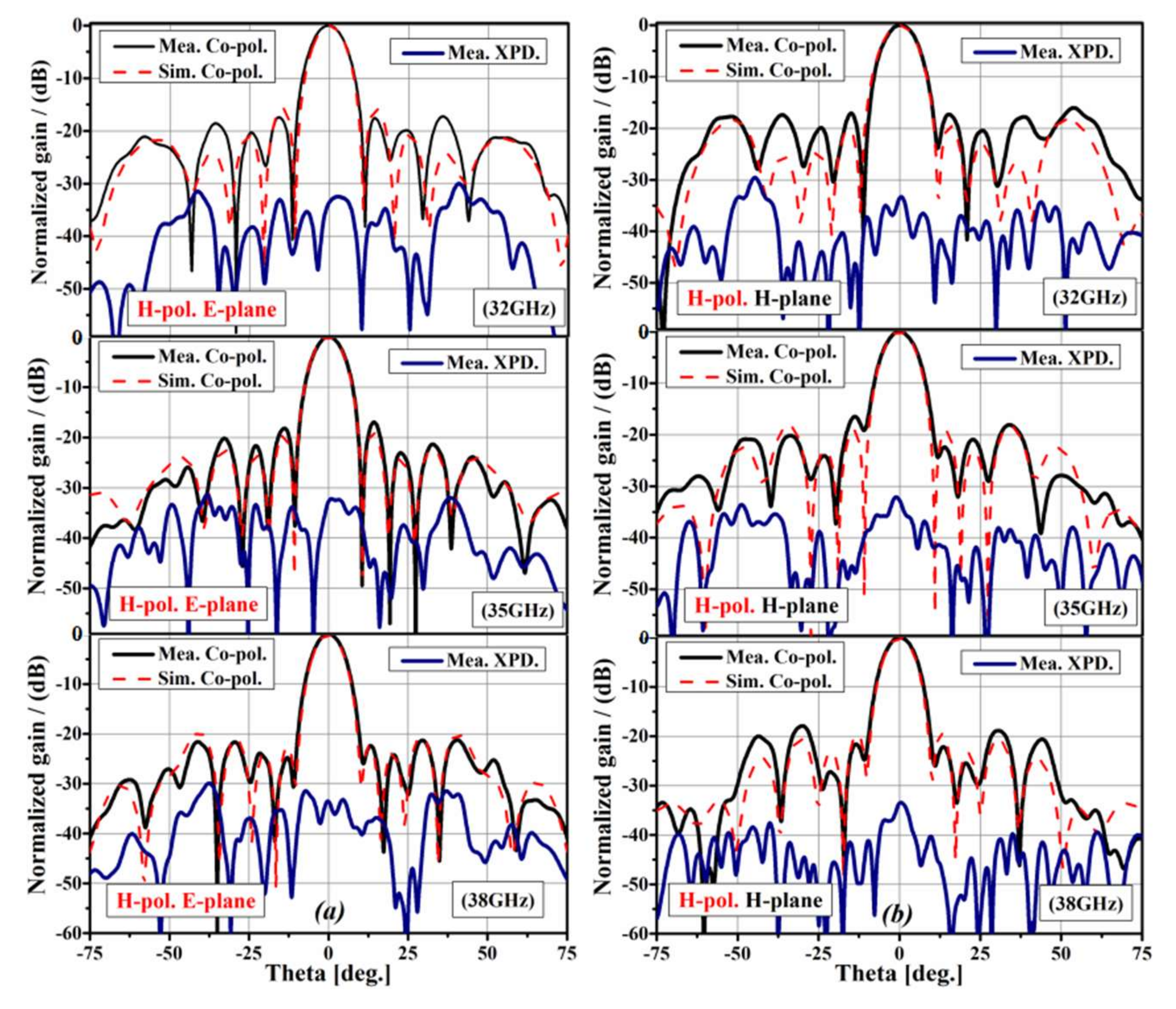
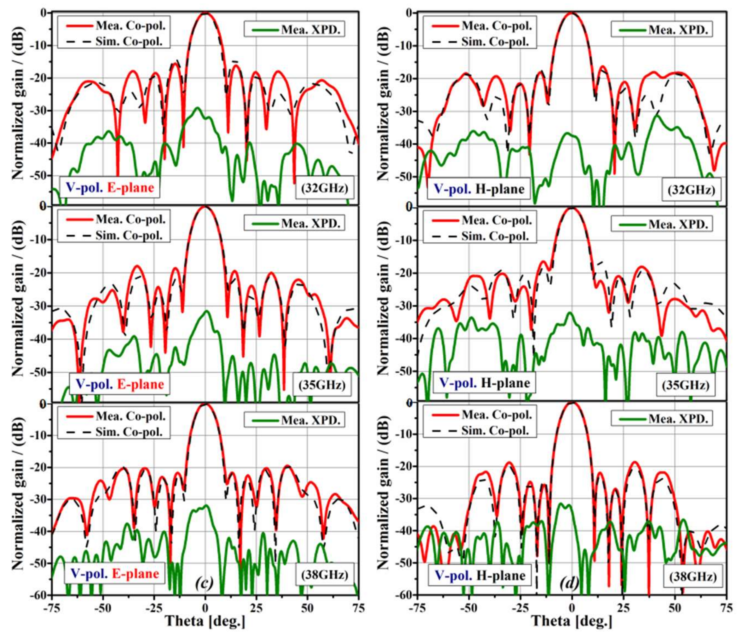
3.2. Measurement of the 8 × 8-Unit ME-Dipole Antenna Array

To verify the validity of the proposed antenna array, a prototype of the 8 × 8-unit dual-polarization ME-dipole antenna array was fabricated and tested. The prototype of the proposed dual-polarization 8 × 8-unit ME-dipole antenna array was printed by the direct metal laser sintering process with a printing accuracy of 100 um, which is shown in Figure 10a,b. Aluminum alloy AlSi10Mg powder was used as the printing material. The top layer and the last three layers were printed and assembled by 12 M3 screws. Two positioning pins of φ = 1.6 mm were used to ensure an interlayer alignment accuracy of ±0.03 mm. The printing accuracy and assembling errors were taken into consideration during the design and analyzed by HFSS to ensure better performance of the array. An SRWG to WR-28 standard WG vertical transition and a bend RWG to WR-28 WG transition were invented as the feed ports. The dimension of the antenna array is 67.5 mm × 67.5 mm × 6.25 mm.
The S-parameter was measured by an Agilent E8361A Vector Network Analyzer. Radiation performance was evaluated by a near-field antenna measurement system at the Ka-band. The measured and simulated s-parameters and gains are plotted in Figure 11. The measured results agree well with the simulations. The measured reflection coefficients less than –10 dB bandwidth for the H-pol. and V-pol. ports are 14.3% (32.4–37.4 GHz) and 17.1% (32.4 –38.4 GHz), respectively. The isolation between the two polarization feed ports is better than 30 dB in the range of 32–38 GHz. The measured gains of the H-pol. array and V-pol. array are higher than 25.8 dBi and 26.1 dBi over the bandwidth of 31–39 GHz. The measured gain is lower than the simulated value by 0.4–0.7 dB. The main reason for the difference in gain comes from the surface roughness of the 3D-printing part. According to previous similar works [19,20,21], the inner surface roughness of the feed networks under the DMLS process used in this design is about 10 um. The loss caused by the surface roughness could be calculated in terms of the reduction of aluminum alloy electrical conductivity. Another simulation of the total array was performed by HFSS to verify the gain differences. The aluminum alloy conductivity in the simulation model is set to 1 × 10⁷ S/m (original value is 3.2 × 10⁷ S/m). The simulated gain vs. frequency curve of the 8 × 8-unit ME-dipole antenna array is also given in Figure 11. The results show that the loss caused by the surface roughness at 32–38 GHz can be estimated to be 0.3–0.5 dB. In addition, tolerances for fabrication and measurement can also cause a slight gain difference. The estimation method can be used in large-scale array design.
The measured radiation patterns in the E-plane and H-plane are shown in Figure 12. The measured first sidelobe levels of the two polarization arrays are less than –17.5 dB in both the E-plane and the H-plane, respectively. The cross-polarization levels are better than 32 dB for the two polarization arrays in both planes. The measured and the simulated radiation patterns are in good agreement, which verifies the effectiveness of the design.
Table 2 compares the measured performances of this work with that of the reported planar dual-polarization mm-wave antenna arrays. Compared with [7,10], this work shows better SLL and XPD. By comparison with the series-feed waveguide slot arrays in [10,13,18], the proposed array has wider impedance-matching bandwidth. Compared with [21], this work exhibits high isolation and XPD. In summary, the proposed dual-polarization ME-dipoles antenna array features high-gain, wideband and low-SLL characteristics with high isolation and XPD.

4. Conclusions

A Ka-band dual-polarization 8 × 8-ME-dipole antenna array based on 3D-printing technology with wideband and low-sidelobe-level features is presented. A novel dual-polarization subarray with 2 × 2-unit ME-dipoles, which consist of cross-slots and metal posts, is proposed. The square OMT and pyramid horn structure is utilized to excite the subarray. A square WG to cross-slots transition structure is invented to connect the radiation part with the feed part. Measured reflection coefficients less than –10 dB bandwidth for the H-pol. and V-pol. ports are 14.3% and 17.1%, with a realized gain higher than 25.8 dBi and 26.1 dBi, respectively. The measured first sidelobe level is less than –17.5 dB, and the cross-polarization discrimination is higher than 32 dB for both arrays. Isolation between the two polarization ports is higher than 30 dB. Featuring wideband and low-sidelobe characteristics, as well as low fabrication cost, the proposed dual-polarization ME-dipole array would be valuable for mm-wave polarization-agile radar and communication systems.

Author Contributions

Conceptualization, Y.W. and H.L.; methodology, H.L. and Y.W.; software, W.T. and K.Z.; validation, K.Z. and W.T.; formal analysis, H.L. and Y.W.; investigation, Y.W.; resources, Y.W.; data curation, Y.W. and H.L.; writing—original draft preparation, Y.W.; writing—review and editing, H.L. and G.Z.; visualization, Y.W. and H.L.; supervision, H.S.; project administration, H.L. All authors have read and agreed to the published version of the manuscript.

Funding

This research received no external funding.

Conflicts of Interest

The authors declare no conflict of interest.

References

  1. Galletti, M.; Bebbington, D.H.O.; Chandra, M.; Borner, T. Measurement and Characterization of Entropy and Degree of Polarization of Weather Radar Targets. IEEE Trans. Geosci. Remote Sens. 2008, 46, 3196–3207. [Google Scholar] [CrossRef]
  2. Gogineni, S.; Nehorai, A. Polarimetric MIMO Radar with Distributed Antennas for Target Detection. IEEE Trans. Signal Process. 2010, 58, 1689–1697. [Google Scholar] [CrossRef]
  3. Wang, Y.; Du, Z. Dual-Polarized Slot-Coupled Microstrip Antenna Array with Stable Active Element Pattern. IEEE Trans. Antennas Propag. 2015, 63, 4239–4244. [Google Scholar] [CrossRef]
  4. Yang, Q.; Gao, S.; Luo, Q.; Wen, L.; Liu, Y. Millimeter-Wave Dual-Polarized Differentially Fed 2-D Multi-beam Patch Antenna Array. IEEE Trans. Antennas Propag. 2020, 68, 7007–7016. [Google Scholar] [CrossRef]
  5. Karimkashi, S.; Zhang, G. A Dual-Polarized Series-Fed Microstrip Antenna Array with Very High Polarization Purity for Weather Measurements. IEEE Trans. Antennas Propag. 2013, 61, 5315–5319. [Google Scholar] [CrossRef]
  6. Cheng, Y.J.; Wang, J.; Liu, X.L. 94 GHz Substrate Integrated Waveguide Dual-Circular-Polarization Shared-Aperture Parallel-Plate Long-Slot Array Antenna with Low Sidelobe Level. IEEE Trans. Antennas Propag. 2017, 65, 5855–5861. [Google Scholar] [CrossRef]
  7. Chen, Z.; Liu, H.; Yu, J.; Chen, X. High Gain, Broadband and Dual-Polarized Substrate Integrated Waveguide Cavity-Backed Slot Antenna Array for 60 GHz Band. IEEE Access 2018, 6, 31012–31022. [Google Scholar] [CrossRef]
  8. Li, W.; Tang, X.; Yang, Y. Design and Implementation of SIW Cavity-Backed Dual-Polarization Antenna Array with Dual High-Order Modes. IEEE Trans. Antennas Propag. 2019, 67, 4889–4894. [Google Scholar] [CrossRef]
  9. Luk, K.M.; Hang, W. A new wideband unidirectional antenna element. Int. J. Microw. Opt. Technol. 2006, 1, 35–44. [Google Scholar]
  10. Li, Y.; Wang, C.; Guo, Y.X. A Ka-Band Wideband Dual-Polarized Magnetoelectric Dipole Antenna Array on LTCC. IEEE Trans. Antennas Propag. 2020, 68, 4985–4990. [Google Scholar] [CrossRef]
  11. Li, Y.; Luk, K. 60-GHz Dual-Polarized Two-Dimensional Switch-Beam Wideband Antenna Array of Aperture-Coupled Magneto-Electric Dipoles. IEEE Trans. Antennas Propag. 2016, 64, 554–563. [Google Scholar] [CrossRef]
  12. Li, T.; Meng, H.; Dou, W. Design and Implementation of Dual-Frequency Dual-Polarization Slotted Waveguide Antenna Array for Ka-Band Application. IEEE Antennas Wirel. Propag. Lett. 2014, 13, 1317–1320. [Google Scholar]
  13. RGatti, V.; Rossi, R. A Dual-Polarization Slotted Waveguide Array Antenna with Polarization-Tracking Capability and Reduced Sidelobe Level. IEEE Trans. Antennas Propag. 2016, 64, 1567–1572. [Google Scholar]
  14. Luo, H.; Xiao, Y.; Lu, X.; Sun, H. Design of a Dual-Polarization Single-Ridged Waveguide Slot Array with Enhanced Bandwidth. IEEE Antennas Wirel. Propag. Lett. 2019, 18, 138–142. [Google Scholar] [CrossRef]
  15. Kim, D.; Zhang, M.; Hirokawa, J.; Ando, M. Design and Fabrication of a Dual-Polarization Waveguide Slot Array Antenna with High Isolation and High Antenna Efficiency for the 60 GHz Band. IEEE Trans. Antennas Propag. 2014, 62, 3019–3027. [Google Scholar] [CrossRef]
  16. Kim, D.; Hirokawa, J.; Ando, M.; Takeuchi, J.; Hirata, A. 64×64-Element and 32×32-Element Slot Array Antennas Using Double-Layer Hollow-Waveguide Corporate-Feed in the 120 GHz Band. IEEE Trans. Antennas Propag. 2014, 62, 1507–1512. [Google Scholar] [CrossRef]
  17. Ferrando-Rocher, M.; Herranz-Herruzo, J.I.; Valero-Nogueira, A.; Bernardo-Clemente, B. Dual Circularly Polarized Aperture Array Antenna in Gap Waveguide for High-Efficiency Ka-Band Satellite Communications. IEEE Open J. Antennas Propag. 2020, 1, 283–289. [Google Scholar] [CrossRef]
  18. Ferrando-Rocher, M.; Herranz-Herruzo, J.I.; Valero-Nogueira, A.; Bernardo-Clemente, B.; Zaman, A.U.; Yang, J. 8 × 8 Ka-Band Dual-Polarized Array Antenna Based on Gap Waveguide Technology. IEEE Trans. Antennas Propag. 2019, 67, 4579–4588. [Google Scholar] [CrossRef] [Green Version]
  19. Li, Y.; Ge, L.; Wang, J.; Ai, B.; Chen, M.; Zhang, Z.; Li, Z. A Ka-Band 3-D-Printed Wideband Stepped Waveguide-Fed Magnetoelectric Dipole Antenna Array. IEEE Trans. Antennas Propag. 2020, 68, 2724–2735. [Google Scholar] [CrossRef]
  20. Sun, F.; Li, Y.; Ge, L.; Wang, J. Millimeter-Wave Magneto-Electric Dipole Antenna Array with a Self-Supporting Geometry for Time-Saving Metallic 3-D Printing. IEEE Trans. Antennas Propag. 2020, 68, 7822–7832. [Google Scholar] [CrossRef]
  21. Zhou, S.; Huang, G.; Chio, T. A Lightweight, Wideband, Dual-Circular-Polarized Waveguide Cavity Array Designed with Direct Metal Laser Sintering Considerations. IEEE Trans. Antennas Propag. 2018, 66, 675–682. [Google Scholar] [CrossRef]
  22. Sun, F.; Li, Y.; Wang, J.; Ma, Y.; Ge, L.; Ai, B.; He, R. A Millimeter-Wave Wideband Dual-Polarized Antenna Array with 3D-Printed Air-Filled Differential Feeding Cavities. IEEE Trans. Antennas Propag. 2021. [Google Scholar] [CrossRef]
  23. Luo, H.; Xiao, Y.; Tan, W.; Gan, L.; Sun, H. A w-band dual-polarization slot array antenna with low sidelobe level. Appl. Comput. Electromagn. Soc. J. 2019, 11, 1711–1718. [Google Scholar]
Figure 1. Dual-polarization ME-dipole unit: (a) planar patches; (b) square posts.
Electronics 10 02969 g001
Figure 2. E-field and surface current distribution of the dual-polarization ME-dipole unit: surface current distributions at (a) t = 0 and (b) t = T/4; E-field distributions at (c) t = 0 and (d) t = T/4.
Electronics 10 02969 g002
Figure 3. Configuration of the dual-polarization 2 × 2-unit ME-dipole subarray: (a) perspective view; (b) top view; (c) details of the OMT.
Electronics 10 02969 g003
Figure 4. E-field distribution of the dual-polarization 2 × 2-unit ME-dipole subarray: (a,b) H-pol; (c,d) V-pol.
Electronics 10 02969 g004
Figure 5. Parameter analysis of the subarray: (a,b) length of cross-slots; (c,d) distance between the ME-dipole units; (e,f) heights of the square WG to cross-slots transition structure.
Electronics 10 02969 g005
Figure 6. Parameter analysis of the feeding part: (a,b) width of square WG; (c,d) height of the pyramid horn cavity; (e,f) width of the coupling window.
Electronics 10 02969 g006
Figure 7. Simulated performances of the dual-polarization ME-dipole subarray: (af) radiation patterns; (g) S-parameters and gain.
Electronics 10 02969 g007
Figure 8. Basic units of the two power-tapering feed networks: (a) UPEP RGWG H-T-junction; (b) UPEP RWG E-T-junction.
Electronics 10 02969 g008
Figure 9. Configuration and simulated performance of the power-tapering feed networks: (a,b) H-pol. feed networks; (c,d) V-pol. feed networks.
Electronics 10 02969 g009
Figure 10. Photograph of the fabricated 8 × 8-unit ME-dipole antenna array: (a) perspective view; (b) prototype of the dual polarization array.
Electronics 10 02969 g010
Figure 11. S-parameters and gain of the 8 × 8-unit dual-polarization ME-dipole antenna array: (a) performance of the H-pol. array; (b) performance of the V-pol. array.
Electronics 10 02969 g011
Figure 12. Measured and simulated radiation patterns of the 8 × 8-unit dual-polarization ME-dipole antenna array: (a) H-pol. E-plane; (b) H-pol. H-plane; (c) V-pol. E-plane; (d) V-pol. H-plane.
Electronics 10 02969 g012aElectronics 10 02969 g012b
Table 1. Details of the proposed dual-polarization 2 × 2-unit ME-dipole subarray (unit: mm).
ParameterValueParameterValue
hp3.5hs1.5
ht2.6hh7.8
wc11.8wp1.3
ws3.3lh5.9
xd6.5au5.2
bu1.6hu0.35
wu1.65hc9.5
ac5.3wd1.6
ad3bd2
ain0.6bin1.4
Table 2. Performance comparison of the presented planar dual-polarization antenna arrays (unit: mm).
Ref.f0
(GHz)
B.WNum. of UnitAperture Size (λ0)Fabrication TechnologyMax.
Gain
Max Rad.
Efficiency
SLL
(dB)
XPD.
(dB)
Iso.
(dB)
[7]6018%
17.1%
8 × 85.4 × 5.4Multilayer PCB22.3 dBi72.5%−131934.7
[10]3257%
45%
4 × 4N.A.LTCC16.1 dBi83%−131514
[12]35
30
1.9%
2.2%
8 × 10
9 × 10
7.6 × 10
8.8 × 11.6
Vacuum brazing25.4 dBi
24.8 dBi
43.05%
36.3%
−17.62540
[13]14.256.1%8 × 2424.4 × 9.5Machining32.4 dBi85%−132310
[18]30.24.9%8 × 87 × 7Machining27 dBi80%−131550
[21]13.519%16 × 1612.7 × 12.7DMLS32.3 dBi55%−131515
This work3514.3%
17.1%
8 × 87 × 7DMLS26.8 dBi73.2%−17.53230
Publisher’s Note: MDPI stays neutral with regard to jurisdictional claims in published maps and institutional affiliations.

