2. Fabrication
For the fabrication of aluminum tunnel junctions, we used three different technologies: Dolan’s technique [
4], bridge-free technology [
5,
6] and direct write technology with magnetron sputtering [
7]. The description and comparison of such technologies are presented in [
8].
To avoid magnetic flux penetration, the first obvious decision is increasing film thickness to over ξ
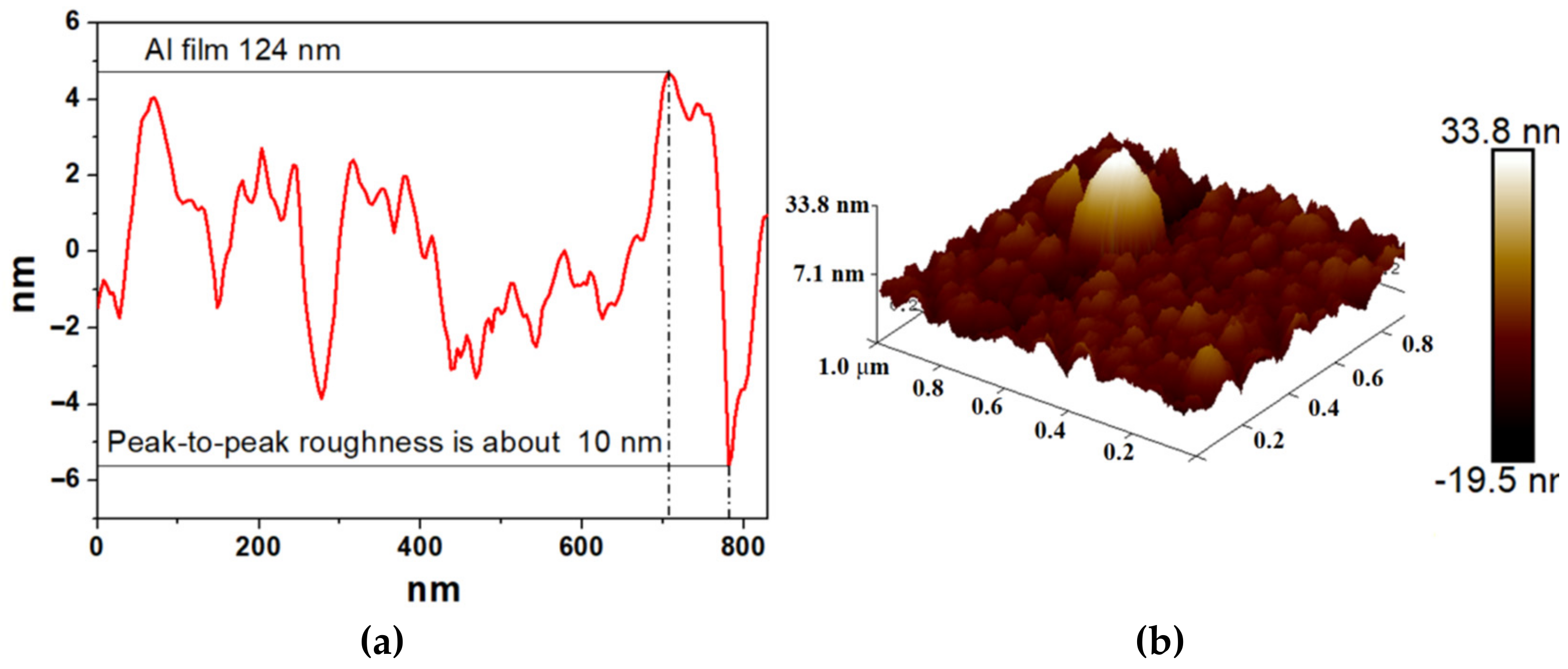
0 or even λ, i.e., 15–100 nm. However, such increase can be accompanied with an increase in grain size, and grain boundaries can become traps for frozen vortices. Reducing the grain size or making the film surface flatter can be achieved by producing epitaxial films on an appropriate substrate with a lattice period close to that of aluminum. Surface roughness is a good indicator of film quality. In the following, we compare several different films deposited by thermal evaporation from resistive boat [
1], electron beam evaporation (
Figure 1), and magnetron sputtering (
Figure 2). Morphological analysis using an Atomic Force Microscope (AFM) was carried out through a Bruker Dimension Icon AFM, equipped with a Nanoscope V controller operated in PeakForce mode. The measurements were performed using N-doped Si probes (Bruker Scanasyst-air).
For 20 and 6 nm-thick films prepared by thermal evaporation, the peak-to-peak roughness was ±2 and ±0.5 nm [
1]. If we take into account that the Al
2O
3 tunnel barrier thickness for our junctions of 1 kΩ × μm
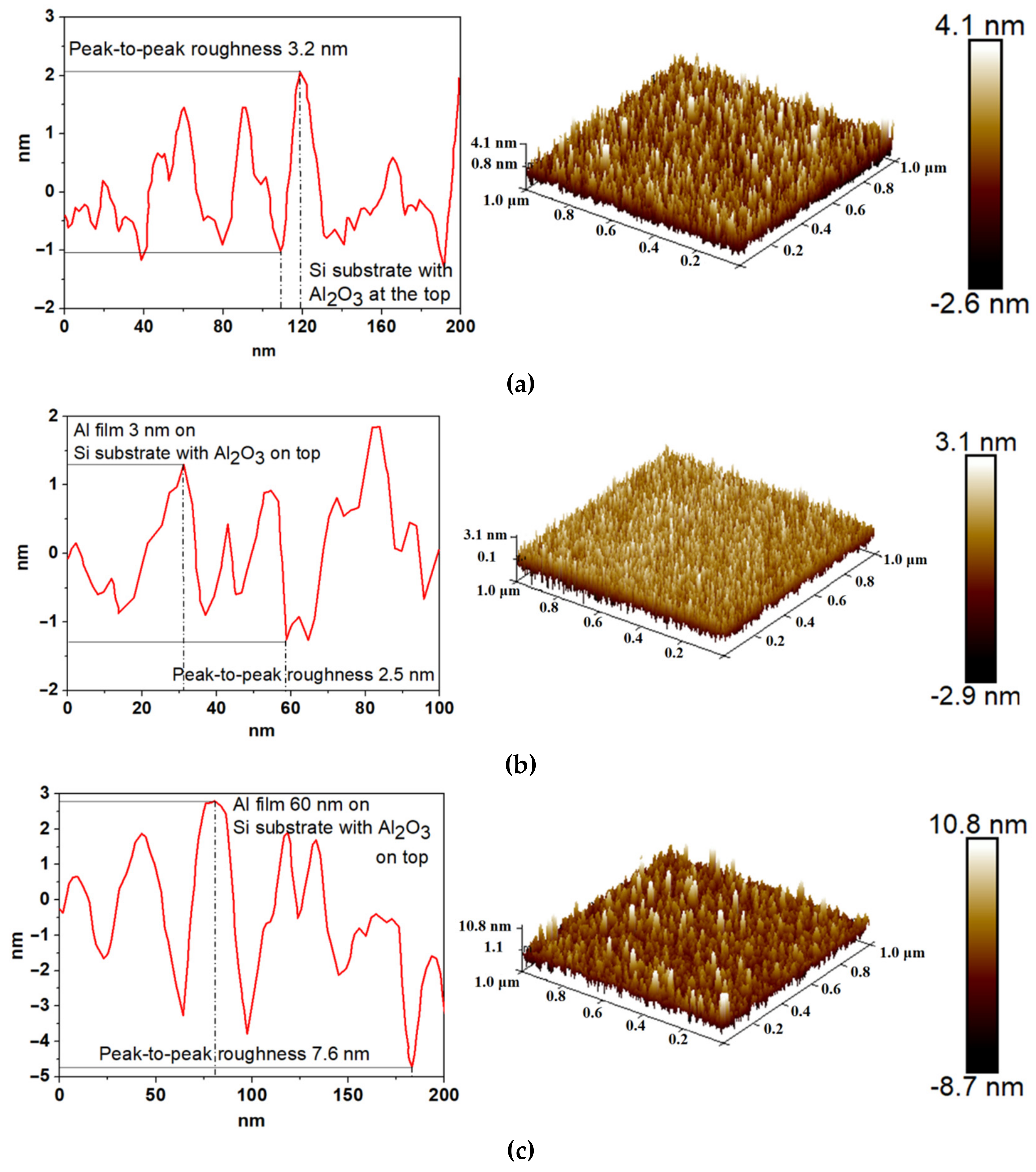
2 was approximately 1.8 nm, it means that a higher quality of NIS junctions can be obtained with thin films of absorbers below 10 nm. The AFM analysis of Al films of 3 and 6 nm thick deposited by magnetron sputtering is presented in
Figure 2. The top layer of superconducting aluminum should be over 150 nm (
Figure 3a). The best-quality NIS junctions with large and thick superconducting electrodes approach resistance R(0)/R(V
2Δ) factor ratio of 1000 at 0.3 K and over 10,000 at 0.1 K (
Figure 3b).
The comparison of peak-to-peak roughness and average grain width for films of different thickness fabricated by three methods is presented in
Table 1.
The overall features of films are not very much dependent on substrate roughness and fabrication method. For films 20 nm and thinner peak-to-peak roughness is about a half of thickness, grain size about twice as much. For 60 and 124 nm films p/p roughness is 10 nm and below, grain size close to the thickness. Films 150 nm and thicker are smoother with roughness on average 5 nm and below and grain size about 500 nm. Such behavior in some way is correlated with critical temperature variations that is 1.2 K for thick films and can increase up to about 1.9 K for thin films. Possible mechanisms of superconductivity in such films will be studied by measurements of IV curves of tunnel junctions fabricated of such films. We also fabricated SIS junctions with the similar layout [
8,
9]. The difference in SIS fabrication is that only Al is deposited as the first layer, contrary to NIS junctions for which the underlayer of 1–2 nm of Fe was deposited before Al. Influence of magnetic field on SIS junction is more complicated, including oscillations of Josephson critical current of SIS junction and penetration of Abrikosov vortices in lower Al layer, as well as in upper Al film. Contrary to SIS, in NIS junctions we have only one effect of vortices in upper Al film that makes explanation clear and unambiguous.
3. Influence of Permanent Magnetic Field on Conductivity of NIS Junctions
To characterize the obtained aluminum films, it is important to study them in a magnetic field. This makes it possible to judge how much their properties correspond to those of bulk aluminum. Pure thick aluminum is a type-1 conventional superconductor with a critical temperature of T
c = 1.2 K, critical field of B
c = 11 mT, coherence length of ξ
0 = 1.5 μm, and magnetic field penetration depth of λ
0 = 15 nm. The grain structure of actual thin films depends on the film thickness and deposition method, in addition to potential contamination. Earlier in our experiments, in the magnetic field normal to the film plane, a nonlinearity at up to ~30 mT was observed, which is above the critical field for bulk aluminum [
2]. This means that Al films of 80 nm thick are not type-1 superconductors.
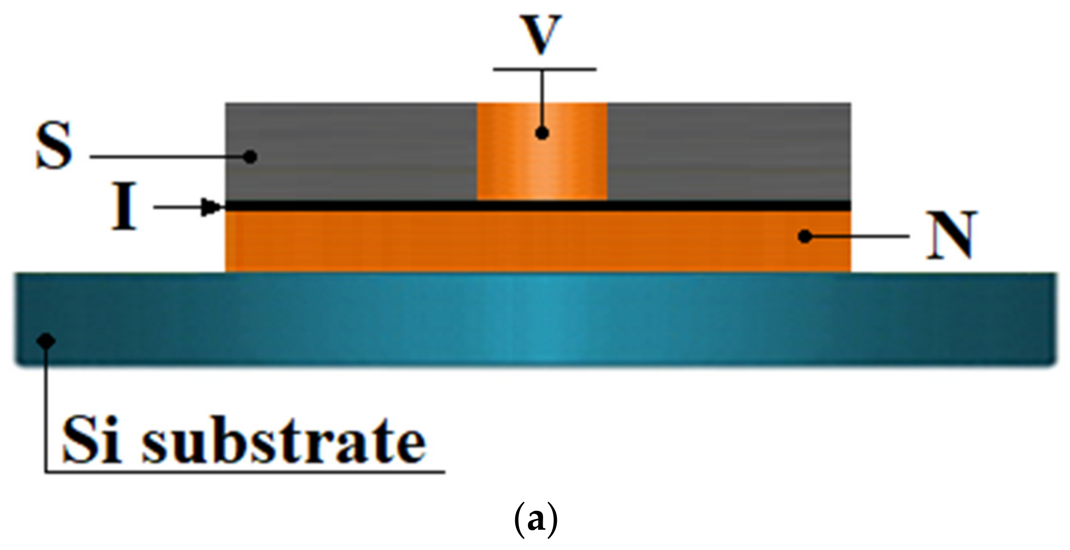
In our experiments, the influence of the magnetic field was observed for single NIS, as well as for SINIS structures, including those integrated into planar antennas. In all cases, at temperatures of 0.1–0.3 K in fields of 10–30 mT at low bias voltages, an increase in the conductivity from tens to hundreds of times was observed. However, the analysis of the results in these cases is complicated by their noticeable overheating by parasitic background thermal radiation from the environment. The most immune to external noise and interferences are the multijunction NIS thermometers with 100 elements connected in series. We studied in detail the influence of magnetic field on the multijunction NIS thermometer. It contains unit cells of five parallel-connected identic NIS junctions connected in series of
n = 100 such parallel cells. A single junction in the thermometer comprised an aluminum electrode covering an oxidized normal electrode made of aluminum with an Fe underlayer for the suppression of superconductivity. Dimensions of the tunnel junction are S
NIS = 1.8 × 1 μm
2, and aluminum thickness is 80 nm. Each junction is connected to Au wiring film of 14 × 100 × 0.1 = 140 μm
3. During the measurements, the structures were cooled down to a temperature of ~ 0.1 K in a portable dilution cryostat [
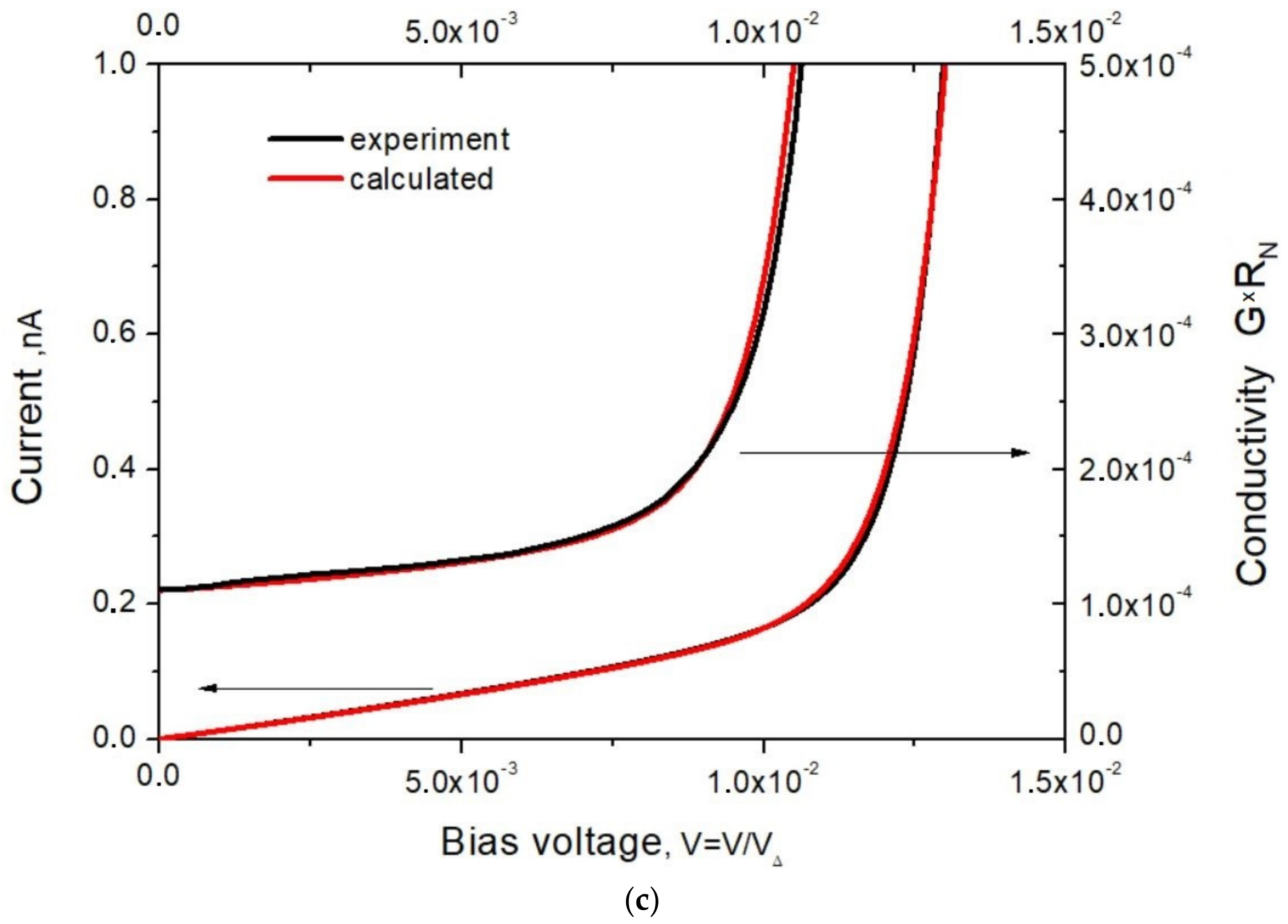
10]. The temperature was measured with a resistance thermometer based on a planar RuO resistor calibrated by a paramagnetic salt thermometer. The IV curves were measured under computer control in the current bias mode set by a 16-bit DAC. The measured voltage was amplified and digitized with a 16-bit ADC. The IV curve at 0.096 K is presented in
Figure 4. A constant magnetic field perpendicular to the substrate was created by a solenoid located outside the cryostat. The superconducting gap Δ
c/k =2.07K (V
Δ = Δ
c/e = 178 μV) and R
n = 9 kΩ were estimated from dynamic resistance measured at a temperature in the range 0.4–0.1 K.
A specific feature of the IV curves is the large impact of the subgap current at bias voltages below 0.5 × n × Δ
c. This can be attributed to Andreev’s current, which can be described according to [
11] by the expression for n junctions in series:
with three fitting parameters that should be selected from experiment [
12]. An alternative approach is the Dynes model [
13]. Initially, it was suggested for describing IV curves at bias voltages around the energy gap Δ
c/e. Later, it was also applied to low-voltage regions. In this model, the subgap current is presented as follows:
Contrary to this Dynes model, in (1), the dynamic resistance is linearly dependent on bias voltage at a bias of approximately V = 0, which corresponds to our experimental results (
Figure 4). For this reason, we prefer to use (1) for describing our IV curves.
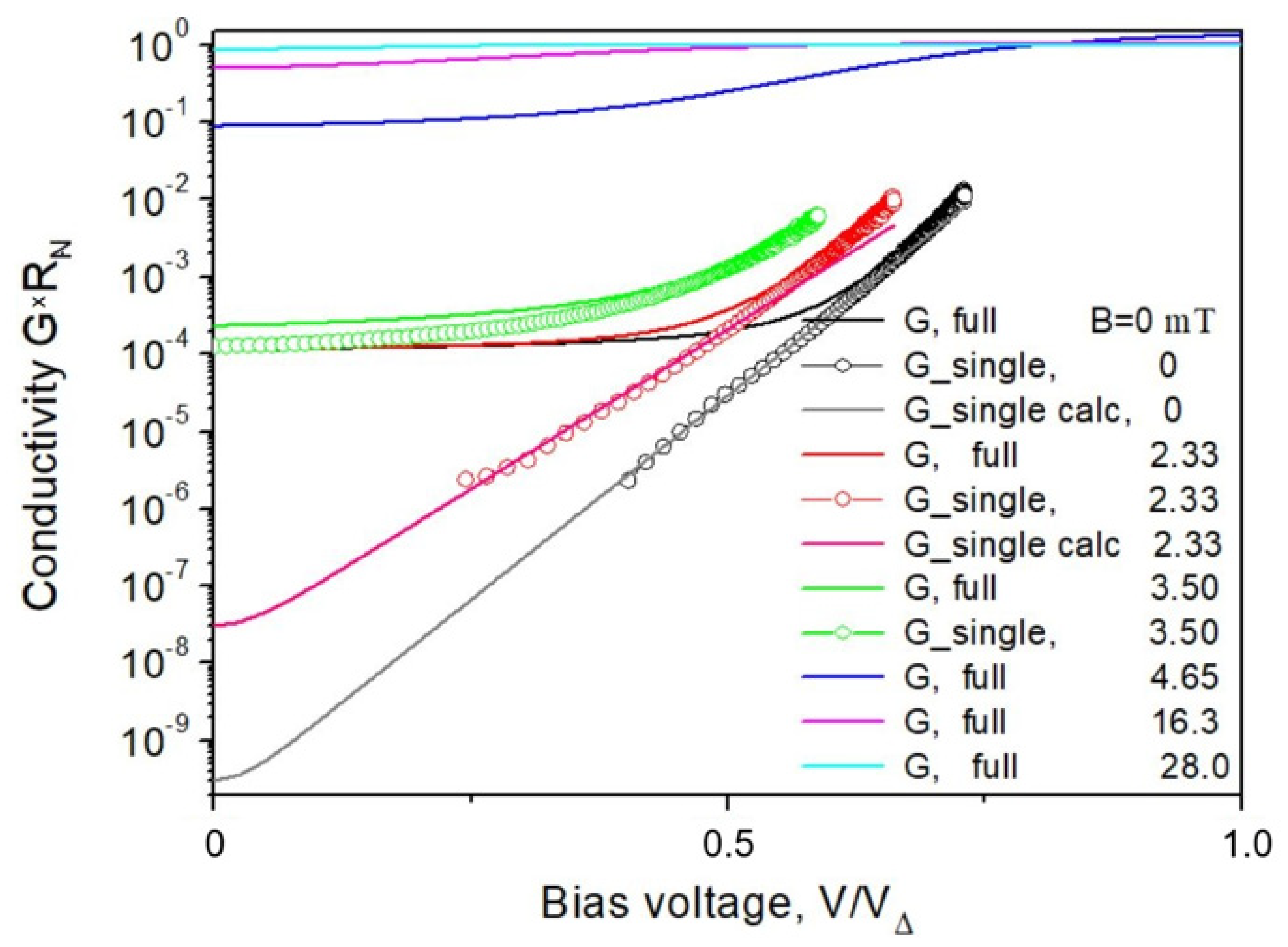
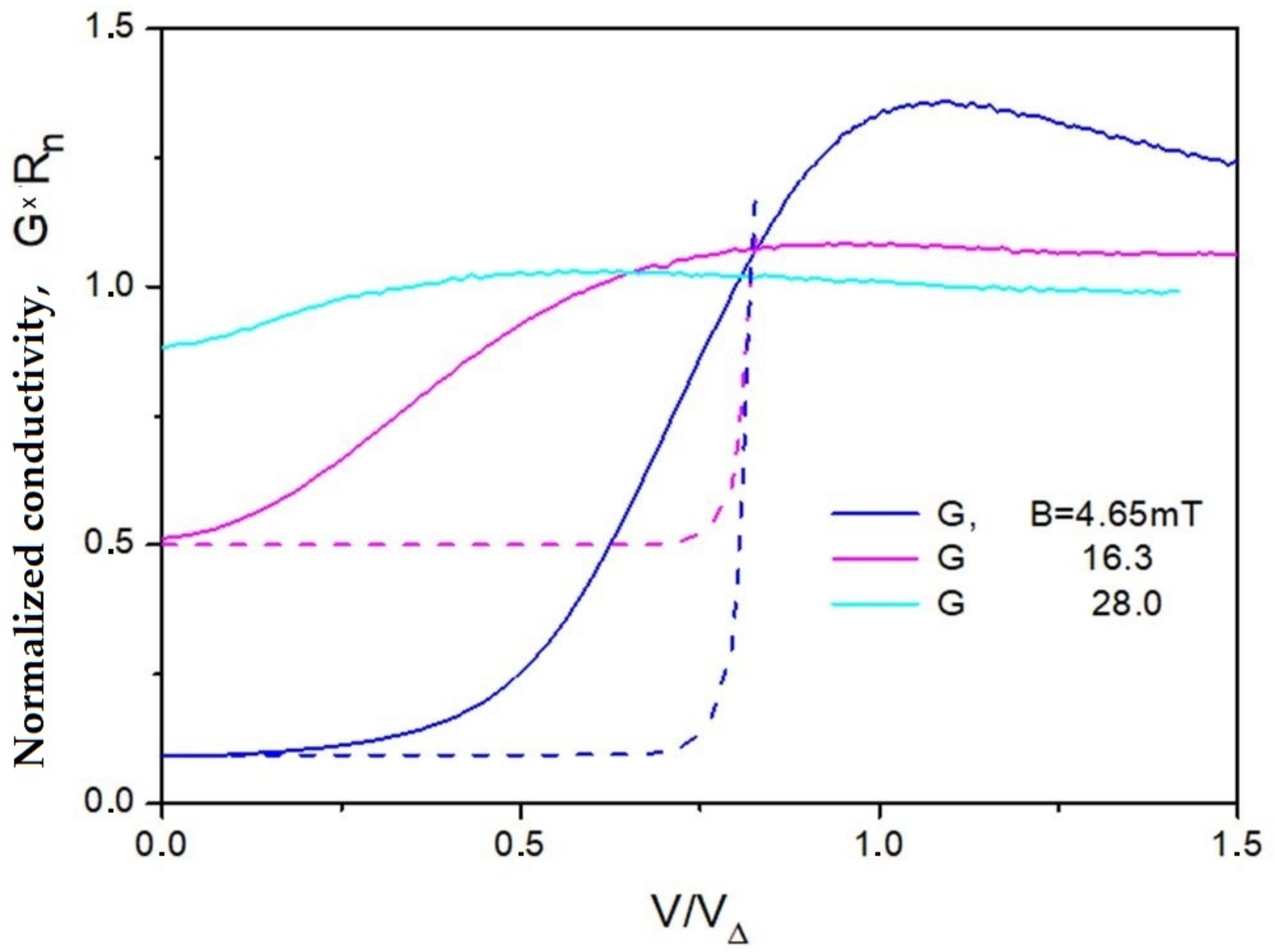
The variation of conductivity in the normal to surface magnetic field is presented in
Figure 5 and
Figure 6 in logarithmic and linear scale. Relative conductivity G × R
n at zero bias and B = 2.33 mT within noise accuracy is unchanged. Changes in single-electron conductivity can be estimated by differentiating IV curves and subtracting the impact of Andreev’s current. According to [
14] for pure NIS junction at low temperature and low bias the single-electron tunneling current I
sing can be presented in common simple form as
Or more exactly, according to [
15] as
From
Figure 5, it is clear that the magnetic field leads to a reduction in single-electron conductivity by two orders of magnitude, but it is still rather small, at the level of approximately 3 × 10
−8. When cooling in magnetic field of 3.5 mT, the variation is more pronounced; single-electron conductivity increases up to 10
−4, and at 4.65 mT, up to 0.09. For a further increase in the magnetic field, relative conductivity approaches 1. However, for a higher magnetic field of 28 mT, the conductivity is still slightly below unity, nonlinearity and superconductivity are still present, which means that although the critical field is not achieved but is very close to it. Therefore, to estimate the correlation length with an accuracy of ~10%, we can use the value of 30 mT as a critical field B
C2.
Pure aluminum is a conventional type-1 superconductor. The grain structure of actual thin films depends on the film thickness and deposition method, in addition to potential contamination. As a result, such films can be similar to type-2 superconductors with second critical field Bc2 > Bc. On the other hand, Bc2 = Φ0/2ξπ2 in which Φ0 is single magnetic flux quantum. As a result, we estimate ξ = 110 nm, more than an order of magnitude lower compared to bulk Al. The penetration depth in this case is λ = ξ0(Bc2/Bc) = 300 nm. Please note that according to textbooks the London penetration depth for bulk pure aluminum is 50 nm. Corresponding relation λ > ξ, which is typical for a type-2 superconductor.
Two mechanisms responsible for changes of conductivity in the magnetic field are a change in the density of states of the superconductor due to depairing in the magnetic field [
16] and changes in the conductivity in the region of Abrikosov’s vortex, which can be directly measured by scanning tunnel spectroscopy [
17].
In [
16], the tunneling current was measured between a long narrow aluminum strip and the tunnel junction to copper. Side dimensions of the superconductor were significantly below London’s penetration depth λ, and the normal magnetic field was uniform. For this case, tunneling current dependence on magnetic field corresponds to a simple formula for depairing energy Γ/Δ
c = (B/B
0)
2, in which B
0~0.1 T. In our case, the strip width is wider than λ, and the relation should be modified. However, if we compare the results, we can assume that at magnetic fields of 2.33 and 3.5 mT, the depairing mechanism is valid. This means that such fields are below the first critical field B
c1.
For the field of 4.65 mT, conductivity at zero bias becomes three orders of magnitude larger than without the field. This means that the penetration of the magnetic field in the superconductor is completely different. In type-2 superconductors for magnetic fields above the first critical field B > Bc1, the magnetic field penetrates in the form of Abrikosov’s vortices each carrying magnetic flux quantum Φ0 = 2.07 mT × μm2. The region of each tunnel junction with area 1.8 × 1 μm2 for the field of 4.65 mT can contain approximately 4 vortices. In the case of coherence length ξ ~ 110 nm, the area of each vortex is approximately 0.04 μm2, and they cover approximately 9% of the junction area. We can neglect interaction between vortices and assume that conductivity is proportional to the number of vortices. Even in the field of 2.33 mT, if the junction contains only two vortices, the conductivity should be two orders of magnitude above the measured value.
The simplest model that allows us to estimate the vortex conductivity is to assume that the vortex core locally forms a normal metal–insulator–normal metal (NIN) structure; see
Figure 7a. Its normalized conductivity will be πξ
2/S
NIS ≈ 0.021. For fields of 4.65 and 16.3 mT, we obtain the conductivity of 0.085 and 0.31, which, taking into account the roughness of the model, can be considered close to the experimental values; see
Figure 6. If it is just resistive shunting, the shape of conductivity curve will be as in
Figure 6, dashed curves. Experimental curves are sufficiently different; they are not so flat, and additional currents make them similar to dependencies at higher temperatures. It is clear that in addition to simple shunting, there is an additional increase in conductivity at non-zero bias voltage.
The bias dependencies of dynamic conductivity in
Figure 6 resemble conductivity dependencies at different electron temperatures. Additional overheating can be attributed to Joule heating of the whole structure by dc current via NIN shunting junctions. For example, let us estimate the heating of an SINIS with a normal electrode volume of ν = 0.02 μm
3. Each vortex across the NIS area shunts it via the resistance of such NIN junction. Resistance can be obtained from the barrier parameter R
nS = 1 kΩ × μm
2 and kernel area of 0.04 μm
2, which correspond to the resistance of such channel R
kern = 25 kΩ. For one NIN junction with single-vortex resistance R = 25 kΩ, the dissipated power is P = V
2/R, half of which is dissipated in the absorber. The electron temperature at around half-gap bias voltage V = 0.2 mV for the normal metal absorber of the volume ν = 0.02 μm
3 will be T
e = (V
2/2RΣν)
0.2, i.e., approximately T
e = 0.6 K. For presented IV curves at 0, 7, 17, and 28 mT, we expect to have approximately 0, 3, 8, and 14 vortices per square micrometer, so the corresponding electron temperatures at half-gap bias are 100, 400, 500, and 700 mK. Dependencies of the electron temperature on Joule heating via 1, 3, and 9 NIN single normal channels are presented in
Figure 7b. Such strong influence of the magnetic field and huge overheating is unacceptable for practical SINIS receivers, so avoiding the presence of vortices is a strong requirement for junction fabrication.
Here, it is necessary to notice that in SIS junctions with relatively thin Al electrodes, the same effect of magnetic field can lead to similar vortices and leakage bridges with resistance of the order of 25 kΩ and its fractions. If such junctions operate in detectors or parametric amplifiers at millikelvin temperatures, the overheating effect should also be taken into account.
Let us estimate whether overheating by the transport current can affect the dependence of conductivity on bias voltage in a case of an SIN thermometer. Let us consider for definiteness the case B = 4.65 mT, voltage 0.01 V and current 0.7 μA. The power dissipated in the structure is 7 nW. The maximum effect will occur if all this power is dissipated in the normal electrodes. This power is dissipated into the phonon system of the electrodes and the gold wiring, the volume and area of which are enormous compared to those of the normal metal of the tunnel electrode. The total volume of all 100 × 5 gold film is 14 × 100 × 0.1 × 100 × 5 = 7 × 10
4 μm
3. Overheating due to Kapitza resistance can be neglected. We also neglect the temperature gradient along the wiring, assuming that its resistivity is the same as that of gold at room temperature. The estimate for the temperature difference between the regions of the film at 0.1 K is of the order of 10 mK. According to [
17], for a gold film at temperatures below 0.5 K, the electron–phonon interaction constant is Σ = 5–8 × 10
−9 W/μm
3 × K
4. Thus, at P = 7 nW and T
substrate = 0.1 K, we have 7 × 10
−9 = 6.5 × 10
−9 × 7 × 10
4 × (T
4 − 0.1
4) and T = 0.104 K. Thus, the change in the conductivity of a superconductor far from the vortex core remains 3–4 orders of magnitude smaller than for a normal metal, and such a change does not affect the total conductivity of the tunneling junction in the presence of a vortex structure.
A more realistic model can be based on the results of studying vortices by scanning tunneling spectroscopy. In [
18], it was found that the density of states normalized to the density in the middle of the vortex, corresponding to the normal state, at zero bias is described by the dependence
where σ
0—conductivity at V = 0 at long distance from the core of vortex. For the axially symmetric vortex, the full conductivity is σ = ∫σ(r, 0)2πrdr in the area of the radius significantly above ξ. The calculation shows that for r > 5 × ξ (but below the junction area), the result is practically independent of ξ, if σ
0 < 10
−4, which is correct in our case. Due to the dirty aluminum value of ξ = 0.11 μm, according to (3), the conductivity for single vortex is σ = 0.031. For 4 vortices, conductivity will be σ = 0.12, which is close to the measured value of 0.09. However, as measurements at 3.5 and 2.33 mT show, partial penetration of the field in the edge regions of the film can sufficiently change the number of vortices in the area of the tunnel junction. Therefore, a self-consistent calculation of the field distribution is required.
It is rather difficult to describe the dependences G(V) exactly. According to
Figure 6, the conductivity maximum at the voltage around the energy gap V
Δ is significantly smeared and shifted to lower voltages with the increase in the magnetic field. This means that the gap becomes coordinate-dependent and, on average, it decreases. Taking into account that this occurs at sizes comparable to ξ, such a calculation should take into account nonlocal effects.


 ,
, 


