Article

A Highly Robust Binary Neural Network Inference Accelerator Based on Binary Memristors

School of Physics and Technology, Wuhan University, Wuhan 430072, China
*
Author to whom correspondence should be addressed.
Electronics 2021, 10(21), 2600; https://doi.org/10.3390/electronics10212600
Submission received: 14 September 2021 / Revised: 13 October 2021 / Accepted: 14 October 2021 / Published: 25 October 2021
(This article belongs to the Section Microelectronics)

Abstract

:
Since memristor was found, it has shown great application potential in neuromorphic computing. Currently, most neural networks based on memristors deploy the special analog characteristics of memristor. However, owing to the limitation of manufacturing process, non-ideal characteristics such as non-linearity, asymmetry, and inconsistent device periodicity appear frequently and definitely, therefore, it is a challenge to employ memristor in a massive way. On the contrary, a binary neural network (BNN) requires its weights to be either +1 or −1, which can be mapped by digital memristors with high technical maturity. Upon this, a highly robust BNN inference accelerator with binary sigmoid activation function is proposed. In the accelerator, the inputs of each network layer are either +1 or 0, which can facilitate feature encoding and reduce the peripheral circuit complexity of memristor hardware. The proposed two-column reference memristor structure together with current controlled voltage source (CCVS) circuit not only solves the problem of mapping positive and negative weights on memristor array, but also eliminates the sneak current effect under the minimum conductance status. Being compared to the traditional differential pair structure of BNN, the proposed two-column reference scheme can reduce both the number of memristors and the latency to refresh the memristor array by nearly 50%. The influence of non-ideal factors of memristor array such as memristor array yield, memristor conductance fluctuation, and reading noise on the accuracy of BNN is investigated in detail based on a newly memristor circuit model with non-ideal characteristics. The experimental results demonstrate that when the array yield α ≥ 5%, or the reading noise σ ≤ 0.25, a recognition accuracy greater than 97% on the MNIST data set is achieved.

1. Introduction

In recent years, deep learning algorithms such as deep neural networks (DNNs) have achieved great success in a wide range of artificial intelligence (AI) applications, including, but not limited to, image recognition, natural language processing, and pattern recognition [1,2,3,4,5,6,7]. To obtain high computing performance, current DNNs are mainly implemented or accelerated by Von Neumann computer architecture based on traditional circuits such as CPU, GPU, and FPGA [8,9]. Due to the limitation of such computer architecture, these deployments require a large amount of data to be transported between memory and the core computing unit, which costs both huge delay and immense power consumption. In addition, in the post-Moore’s Law era, performance enhancement of DNNs cannot always keep up with the computing requirements and the actual gap increases quickly [10]. Therefore, it is urgent to design new computing architecture to attack the famous memory wall problem.
In 2008, Hewlett Packard (HP) Labs announced that they had experimentally confirmed the existence of memristor, also known as resistive random access memory (RRAM) [11]. Since then, a large number of researchers have been attracted to it because the memristor has beneficial physical properties, such as high scalability, low operating voltage, high endurance, and a large ON/OFF ratio which make it particularly suitable to act as a biological synapse. Furthermore, it has a high degree of circuit integration and can be combined with CMOS technology, showing extremely high feasibility and superiority in the fields of logical computing, neural network and chaotic computing, and has thus become one of the outstanding candidates for the next generation of computing architecture [12,13,14,15]. However, that is not the entire beauty of it. Non-linearity, inconsistent periodicity, and asymmetry in the memristor’s conductance modulation, drift and failure in read/write operation, and other non-ideal factors could cause tremendous difficulties when the memristor is introduced in pattern recognition and other similar AI applications [16,17,18,19]. To solve these problems, one possible method is to improve manufacturing process of memristors to increase device performance, but there is still a long way to go. On the other hand, specific neural network structures matching the performance level of existing memristors will be the most reasonable approach. Binary neural network (BNN) was recently proposed to compress DNNs algorithms with acceptable recognition accuracy into conventional neural networks on various data sets (MNIST [20], CIFAR-10, and so on), and some works have shown it to be promising for accelerating neuromorphic computing [21]. Nowadays, the industries are able to manufacture binary memristors with stable performance, which provides a strong basis to implement memristive binary neural network (MBNN). Compared with analog memristive neural network implementations, MBNN replaces full-precision floating point weights with binarized constants ±1 without any other weight value, then neuron values become binary 0/+1 to adapt and simplify network structure and especially peripheral circuits. In particular, it is suitable for implementation at the existing memristor’s performance level [22]. In addition to allowing storing information and performing computation, there are other advantages to binary memristors being integrated in a highly parallel architecture: good size (down to 2 nm), fast switching (faster than 100 ps), and low energy per conductance update (lower than 3 fJ) [23,24]. Lately, binary memristor-based neuromorphic Integrated Circuits (IC) is gradually becoming a trend of In-Memory Computing. Initial works reported a 16 Mb RRAM Macro Chip using binary memristors, the BNN achieves a relatively high recognition accuracy (96.5% for MNIST) under the non-perfect bit yield and endurance [25]. Another work designed, fabricated, and tested a binary memristor array that could obtain classification accuracies of 98.3%, 87.5%, and 69.7% on MNIST, CIFAR-10, and ImageNet, respectively [26]. These works were mainly based on the differential pair structure, thus, new BNN algorithms and memristive crossbar structures are needed to improve the performance of MBNNs.
The single-column reference structure is applied in previous studies, which can provide nearly 50% area reduction and power saving for a memristive array. Nevertheless, the sneak current effect in this scheme limits the scale of memristive crossbar array [27,28]. More recently, Yi-Fan Qin et al. proposed a binary memristor-based BNN inference accelerator, which demonstrated it is promising to obtain a robust BNN acceleration hardware implementation with less overhead of chip area, energy consumption, peripheral circuit complexity, but theoretically [29].
In this paper, a novel memristive crossbar structure for BNN accelerator with binary sigmoid activation function is proposed. In the accelerator, inputs of each layer of BNN are set to be either +1 or 0, which not only facilitates feature encoding but also reduces peripheral circuit complexity of memristor-based circuits. Its two-column reference memristor together with current controlled voltage source (CCVS) circuit not only solves the problem of mapping positive and negative weights on memristor array, but also eliminates the sneak current effect due to the minimum memristor conductance. Futhermore, compared to the traditional differential pair structure of BNN, the proposed two-column reference scheme can reduce both the number of memristors and the latency to refresh memristor array by nearly 50%. Influence of non-ideal factors of memristor array such as memristor array yield, memristor conductance fluctuation, and reading noise on accuracy of MBNN is investigated in detail based on a new memristor circuit model with non-ideal characteristics. The experimental results demonstrate that when array yield is α ≥ 5%, or reading noise σ ≤ 0.25, recognition accuracy greater than 97% in the MNIST data set can be achieved.

2. Memristive BNN

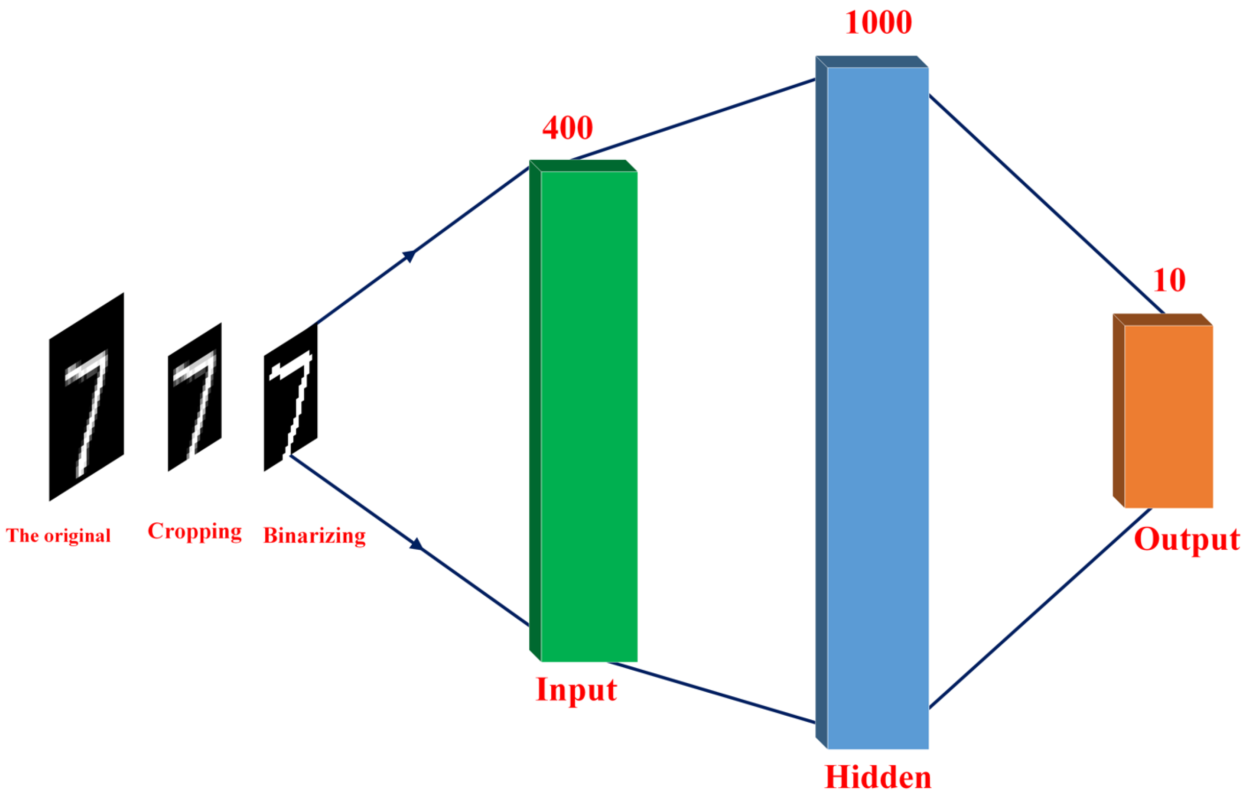
2.1. Binary Neural Network

The full process of the BNN algorithm is shown in Figure 1 [22]. In its forward inference stage, input feature vector X and binary weight matrix W b are multiplied by vector-matrix multiplication (VMM) operations to obtain intermediate value T, where the elements in W b take only two numerical values of either +1 or −1 obtained from a binarization procedure. Then batch normalization (BN) and activation process ∫ are applied to calculate output feature vector Z. Parameter g is the gradient of loss function which includes two variables of output feature Z and its target value Y. While in its training stage, binary weight W b is adopted to calculate weight gradient △W by △W  = f ( W b , g , X i ) . In order to maintain a sufficiently high accuracy of BNN algorithm, 32-bit float point weight matrix W is adopted in the weight updating stage. At the end of the training stage, the following binarization rule is applied to convert the 32-bit float point weight W into binary W b :
W b = S i g n ( W ) = + 1 , W 0 1 , o t h e r w i s e
To facilitate a BNN algorithm suitable for hardware implementation using memristor crossbar, the original BNN algorithm is improved in the following method: input features of the first layer of BNN are from the binarized image pixels of MNIST test data set, that is, we mapped the gray value of the original image pixels into either 0 or 1. Input features of other layers are the intermediate data processed by the activation function of the output from their previous layer, and the binary sigmoid activation function is as follows:
B i n a r y s i g m o i d ( x ) = + 1 , x 0 0 , o t h e r w i s e
In this way, during the inference stage, all features remain as either 0 or 1, which will facilitate the coding of input features and reduce peripheral circuit complexity. The specific coding method is detailed in Section 2.3. In order to accelerate training and obtain better convergence, the sizes of original images are cropped from 28 × 28 to 20 × 20, which is enough to show the performance of our proposed memristor-based network circuit.
The MNIST database contains 70,000 images representing the digits zero through nine. The data are split into two subsets, with 60,000 images belonging to the training set and 10,000 images belonging to the testing set. This kind of separation ensures that given what an adequately trained model has learned previously, it can accurately classify relevant images not previously examined. For all BNNs in this work, 8000 training images are randomly picked from the training dataset (60,000 images) per epoch, and the training process is for 125 epochs. The network topology of BNNs in this work is a kind of multi-layer perceptron (MLP) [30], having single or multiple hidden layers between the input layer and the output layer. All layers in the BNN are fully connected layers where all the inputs from one layer are connected to every unit of the next layer. To match both the size of MNIST test data set and classification goal of 10 digits, the number of input and output neurons of proposed MBNN are 400 and 10, the scale of hidden layers will directly determine network complexity. In general, the larger the network scale, the higher the recognition accuracy will be. Nevertheless, the networks with a larger scale need more time to train. From Figure 2, we find that when the hidden layer has more than 1000 neurons, the recognition accuracy will nearly saturate, meanwhile, the recognition accuracy difference between networks with one and three hidden layers is only about 1%, a slight degradation. Thus, in our work, a 400 (input layer)–1000 (hidden layer)–10 (output layer) MBNN is employed to explore the effects of non-ideal factors. The detailed results are given in Table 1.

2.2. Memristor Model

The model proposed by Pershin et al. [31] has been widely referenced by researches in memristor systems [32,33,34,35] because of its simplicity. So far, researchers have developed many excellent memristor devices which have reliable switching behaviours, high switching ratio, and extended endurance of set/reset cycling processes [36,37,38]. Since we focus on binary memristors rather than analog memristors, utilizing fabricated or measured memristor data could make little improvement in the simulation. In order to obtain fast simulation when BNN is mapped into MBNN, this bipolar threshold voltage memristor model is utilized in our work, which can be expressed by the following equations:
R I = V ( t )
d R d t = f ( V ( t ) ) [ θ ( V ( t ) θ ( R O F F R ) + θ ( V ( t ) θ ( R R O N ) ) ]
f ( V ( t ) ) = β V ( t ) + 0.5 ( α β ) [ | V ( t ) + V T H | | V ( t ) V T H | ]
where I is memristor current, R is memristor resistance, V ( t ) is voltage applied to memristor to modulate its conductance. R O F F is the maximum memristor resistance (i.e., the resistance when the memristor is turned off), and R O N is the minimum memristor resistance (i.e., the resistance when the memristor is turned on); α and β are two critical parameters for adjusting change rate of memristor resistance: When α = 0 , memristor resistance remains unchanged when the applied voltage is less than the threshold voltage V T H . β is used to adjust the resistance change rate when the applied voltage V ( t ) is greater than V T H . The larger β is, the higher the change rate is, or vise versa. θ ( x ) is a step function denoted as:
θ ( x ) = + 1 , x 0 0 , x < 0
The function θ ( x ) constraints memristor resistance between R O F F and R O N .
The model is realized using Verilog-AMS language, and parameters in the model are: R O F F = 200,000 Ω , R O N = 2000 Ω , α = 0 , β = 10 16 , V T H = 4.6 V. 6 V 1000 Hz sinusoidal voltage signal is applied, and the current–voltage (I-V) characteristic curve is shown in Figure 3, where a hysteresis curve shows a nearly ideal memristor switch between OFF and ON state. Memristor conductance modulated by positive and negative voltage with pulse width 100 ns is shown in Figure 4. It can be seen that when the 6 V positive voltage is applied, conductance reaches the maximum value. When applied voltage is less than the threshold voltage of 4.6 V, the conductance value remains unchanged. When the 6 V negative voltage is applied, conductance value becomes the minimum one. All these characteristics make this model suitable for MBNN implementation.

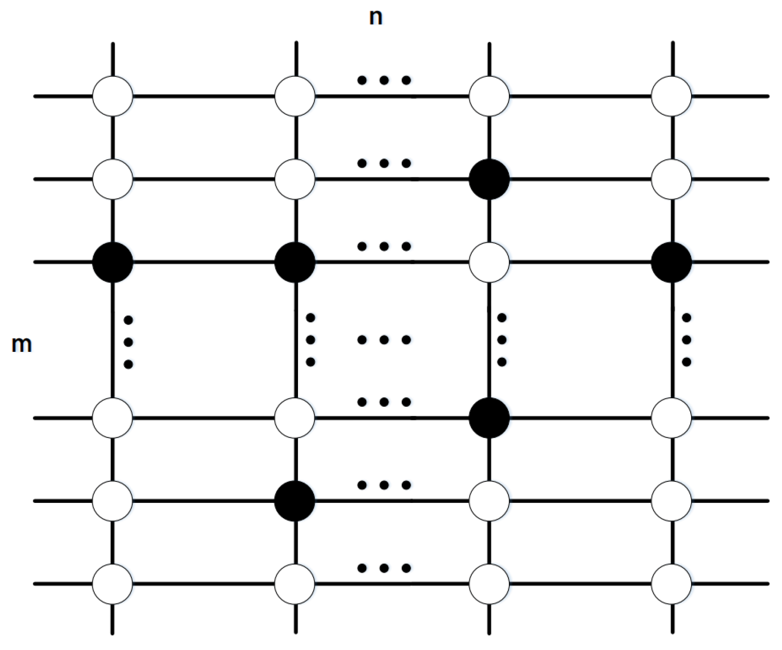
2.3. Implementation of MBNN

In the proposed MBNN, each memristor acts as a synapse in a neural network by applying a certain voltage pulse to modulate its conductance. The weight matrix W m × n is correspondingly represented by the conductance G m × n of memristor array, input feature vector x m × 1 is encoded into voltage signal vector V m × 1 to write into memristor array, and output feature is the current I k of each column of the memristor array, which is expressed as:
I k = i = 1 m V i × G k , i ( k = 1 , 2 , , n )
and it implements VMM functionally as shown in Figure 5.
In the whole forward inference stage of MBNN, weight has only two values: +1 and −1, so we use binary memristor to implement the circuit. Memristor conductance can only be positive, so mapping both positive and negative weights into the memristor array is a critical problem. The three methods shown in Figure 6 are investigated. The traditional differential pair structure is shown in Figure 6a, where the conductance difference of two memristors (a differential pair) is used to represent one synapse, each of the two memristors has two resistive states: high-resistance state (HRS) and low-resistance state (LRS), the corresponding conductance states are denoted as G H R S and G L R S . This is a classic scheme to map positive and negative weights in memristive crossbar array, which is also used in previous work [39,40,41,42]. Differential operation is performed on the two memristors to achieve mapping of the two weight values of +1 and −1, where the output feature, namely the current Ik of each column of memristor array, is expressed as:
I k = i = 1 m V i × ( G k , i + G k , i ) ( k = 1 , 2 , , n )
where G ( k , i + ) and G ( k , i ) can only take two values of G H R S and G L R S , where G H R S G L R S is used to represent the weight value of −1, and G L R S G H R S is used to represent the weight value of +1.
As shown in Figure 6b, The select column scheme was proposed in a previous study, and it can provide nearly 50% area reduction and power saving for a memristive array [27]. Nevertheless, the sneak current effect in this scheme limits the scale of memristive crossbar array, which can be suppressed by the two-column reference memristor scheme proposed in our work. The proposed circuit is shown in Figure 6c, only one memristor is used to realize synapse. In the blue box, there are two columns of reference memristors. The conductance of the two reference columns can be referenced by the conductance of the synapse memristor to realize mapping of the positive and negative weights (+1 and −1). The output characteristic I k can be expressed as:
I k = i = 1 m V i × ( G k , i 1 2 ( G L R S + G H R S ) ) ( k = 1 , 2 , , n )
That is, 1 / 2 × ( G H R S G L R S ) is used to represent the weight value of −1, and 1 / 2 × ( G L R S G H R S ) is used to represent the weight value of +1. It should be pointed out that the output of memristor reference columns is current, and each neuron needs the output of reference columns, which will cause the current to shunt. Thus CCVS circuit is used to convert current signal into voltage signal to solve the current shunting problem. By such design, the number of memristors is reduced by nearly 50% compared to the traditional differential pair structure. In addition, due to the reduction in the number of memristors, the writing time of trained data into the memristor array will also be reduced almost by half. The hardware implementations of the proposed BNN system are similar to the select scheme [19], with the major difference of considering sneak current effect under the minimum conductance status, thereby successfully eliminating the sneak paths induced by minimum conductance states (HRS) of the memristors in the crossbar array, which is a valid method to promote the robustness of MBNN.
The process of the MBNN acceleration circuit is mainly divided into two steps: (1) writing weights; (2) inferencing the result. In the first step of writing weights, memristor conductance can be modulated by voltage pulses, and weights obtained through software training are written into the memristor array. 1T-1M (one transistor and one memristor per cell) is a common model designed for memristive crossbar array to overcome the shortcomings of the conventional 1M model, in which a MOSFET transistor is added to a memristor as a selector to reduce the sneak current effect [43,44]. Compared with 1T-1M crossbar array, 1M crossbar array has a simpler structure, higher integration, and is easier to produce. As the problem of sneak paths has been solved by the proposed two-column reference memristor scheme, a 1M crossbar memristor array is adopted for implementation in our work. For 1M crossbar array, 1/2 voltage bias scheme is adopted to update weights, as shown in Figure 7. In this way, it can be ensured that most memristors in the array maintain 0 V when conductance update is not required, which significantly reduces power consumption. In the actual circuit simulation process, we initialize resistance of the memristor model to the maximum value, so when updating weights, the memristor array can operate column by column to reduce writing time.
In our case, memristors in red will be programmed to +1 when they are biased at Vw and ground, while memristors in blue will be programmed to 0 when they are biased at ground and V w (the so-called 1/2 voltage bias scheme). In the inference phase, the input feature is encoded as voltage pulse series and applied to the memristor array. As mentioned above, we have made improvements to BNN algorithms suitable for memristor array implementation. The input value of each fully connected layer is 0 or +1, so it can be succinctly coded: input feature +1 is coded as voltage V R E A D (0.2 V), and input feature 0 is coded as voltage 0 V. This process can greatly simplify the peripheral circuit design.

3. Results and Analysis

3.1. Simulation Results of the Two Schemes

Verilog-AMS introduces the connect module construct [45]. To facilitate verification of a large digital–analog hybrid circuit, designers could develop models representing the functionality of blocks using modeling constructs in Verilog-AMS. Commonly, these models are simulated in conjunction with the corresponding transistor-level circuit to ensure consistency of the models with the actual implementation of the circuit. [46]. The memristor model, a connect module, provides two ports and has a behavioral description stating the transformation process. In Cadence Virtuoso, the memristors will be automatically arranged to form a crossbar array through a script. Unlike software language descriptions, in this way, circuit simulation could be conducted to low-level and detailed, which is the key to probing and addressing the problem of sneak paths. Both memristive BNNs in Figure 6a,c are carried out via the industry-standard mixed signal circuit design language Verilog-AMS and simulated by Cadence Spectre. Validating feasibility of the proposed memristor circuit especially in real circuit level is our main purpose, so we set the size of neural network for 400(input layer)-100(hidden layer)-10(output layer) to reduce the simulation time which mainly depends on the size of hidden layers. The whole circuit system consists of three voltage sources: the amplitude and period of writing voltage source is 6 V and 0.2 µs respectively; 1/2 writing voltage source is 3 V (i.e., less than 4.6 V voltage threshold of memristor), and has the same 0.2 µs period; reading voltage source is 2 V and also has 0.2 µs period. The initial conductance states of memristors to carry out MBNN are all G H R S , and then the weights for each column of the crossbar are sequentially written into one column each time.
For the traditional differential pair scheme of memristor array, the simulation time is set to (100 × 2 × 0.2 + 10,000 × 0.2) µs = 2040 µs, where 100 is the number of hidden layer neurons, 2 represents the number of memristors required to achieve a synapse, 0.2 µs is voltage writing cycle time. In other words, 40 µs resistance tuning time is required for a network with a scale of 400 × 100 × 10, in which the memristor array between the input layer and the hidden layer and the memristor array between the hidden layer and the output layer are modulated simultaneously. The inference time required to test 10,000 digits of MNIST data set is 2000 µs. As to results, the voltage signals of output neurons are obtained, which correspond to the probability of each possible class of ten 10 digits (0–9), the circuit finally chooses the one with the highest probability as the classification result.
Figure 8 shows waveforms extracted from the output neurons, where at the first 0.2 µs cycle, the maximum magnitude of voltage values indicates that the winner digit is 7, which is consistent with the correct digit, and the same kind of analysis can be applied to the rest of simulations. Overall, the performance of MBNN based on the differential pair scheme is consistent with the software results, and recognition accuracy of 91.8% can be achieved.
For the proposed MBNN with a two-column memristor reference structure, the simulation time is set to (100 + 2) × 0.2 µs + 10,000 × 0.2 µs = 2020.4 µs, where (100 + 2) is the amount of memristor columns needed to be tuned. Figure 9 shows the voltage signals of output neurons, and the recognition accuracy also reaches 91.8%, which is of course also consistent with the software results.
Some comparison are shown in Table 2. It can be seen that the proposed two-column reference scheme utilized 42,000 memristors, which is reduced by as much as 48.78% compared to 82,000 memristors of the traditional differential pair scheme; writing time is 20.4 µs, 49% less than 40 µs of the traditional differential pair scheme. Both of the two schemes have obtained 91.8% recognition accuracy on MNIST data test set. Though the schematics of the two schemes are different, the same BNN algorithm is correctly mapped by both of them respectively and that is the reason why both of them have achieved the same recognition accuracy.

3.2. Non-Ideal Effects on Memristor Crossbar

To speed up the study on non-ideal effects on memristor crossbar of MBNNs, the simulation is futher carried out by a chip-like framework implemented in C++ software [18]. In this case, we considered various non-ideal effects such as yield rate of memristor array, memristor conductance fluctuation, and reading noise in memristor crossbar to evaluate the robustness of the proposed method. Compared with Verilog-AMS approach, the pure-software simulation speed is faster and it is more convenient to analyze the impacts of non-ideal factors.
As shown in Figure 10, the network size to explore non-ideal factors on MBNN is set as 400-1000-10, and recognition accuracy is 97.41% on the MNIST test data set under ideal conditions. This shows that there is no error in mapping of BNN on memristor array, which also proves the superiority of MBNN built in this paper in an undirect way.

3.2.1. Yield Rate of Memristor Array

Commonly, actual memristor array often has device failure problem, for example, resistance value of a memristor could stuck between the maximum resistance and the minimum resistance, regardless of the set or reset operations [47]. The ratio of memristors that can work well to the overall memristors is called yield rate α of array. For example, if a memristor array has a scale of m × n and assuming that its yield rate is α , then the number of memristors that work normally is α ( m × n ) , and the number of failing memristors is ( 1 α ) ( m × n ) , these memristors are assumed evenly distributed in memristor array as shown in Figure 11, where a black dot represents a memristor that cannot work normally, and a white one indicates a memristor that can work well.
Figure 12 shows the effect of memristive array yield on MBNNs with different schemes, and detailed values are given in Table 3. It can be seen that recognition accuracy of both schemes increases along with the yield rate. For the traditional differential pair scheme, when the yield rate is greater than 92%, the recognition accuracy is greater than 97%, and even when the yield rate is 90%, the recognition accuracy is still greater than 96.9%; for the proposed two-column reference scheme, when the memristor array yield rate is greater than 94%, the network recognition accuracy is greater than 97%, even when the yield rate is 90%, the recognition accuracy is still greater than 96.7%. We can also see that when the array yield remains the same, the recognition accuracy of traditional differential pair scheme is slightly better than the proposed two-column reference scheme, which may be due to the differential pair scheme including a large number of memristors. When one memristor in the pair fails, the two memristors constituting a synapse are in the same state, so the contribution current of the differential operation is 0, that is, the weight turns from +1 or −1 to 0. When a memristor fails in the reference column structure, the weight in the two memristors of a synapse changes reversely. In short, both of them have good robustness as to the yield rate of memristor array.

3.2.2. Memristor Resistance Fluctuation

Memristor resistance fluctuation refers to the difference between the target conductance state and the actual conductance state of memristor. This is mainly caused by two reasons: (1) Due to the limitation of manufacturing process, the electrical characteristics of each memristor are not completely consistent, and conductance fluctuates around expected value; (2) Due to the limitation of the working principle of the conductive filament of memristor, when the state of memristor is modulated by voltage pulse, there is a certain difference between the actual state and the target state [48]. Hence, the actual conductance state may be a little smaller or larger than the target state. In our study, we assume that the target conductance state of memristor is G a i m , and the actual conductance state of memristor obeys a normal distribution with the mean value of the target conductance G a i m and the standard deviation is σ . Figure 13 is a schematic diagram of memristor fluctuation in memristor array, where the darker the dot color is, the greater the fluctuation of the memristor is; and the lighter the dot color is, the smaller the fluctuation of the memristor is.
Figure 14 shows that the recognition accuracy of both schemes decreases along with memristor fluctuation increases, and detailed values are given in Table 4. For the traditional differential pair scheme, when σ is smaller than 0.2, the recognition accuracy is greater than 97%. When σ equals 0.5, the recognition accuracy is still close to 90%; for the proposed two-column reference scheme, when σ is smaller than 0.1, the recognition accuracy is greater than 90%. Compared to the traditional structure, MBNN with a two-column reference structure is less robust to the device fluctuation.

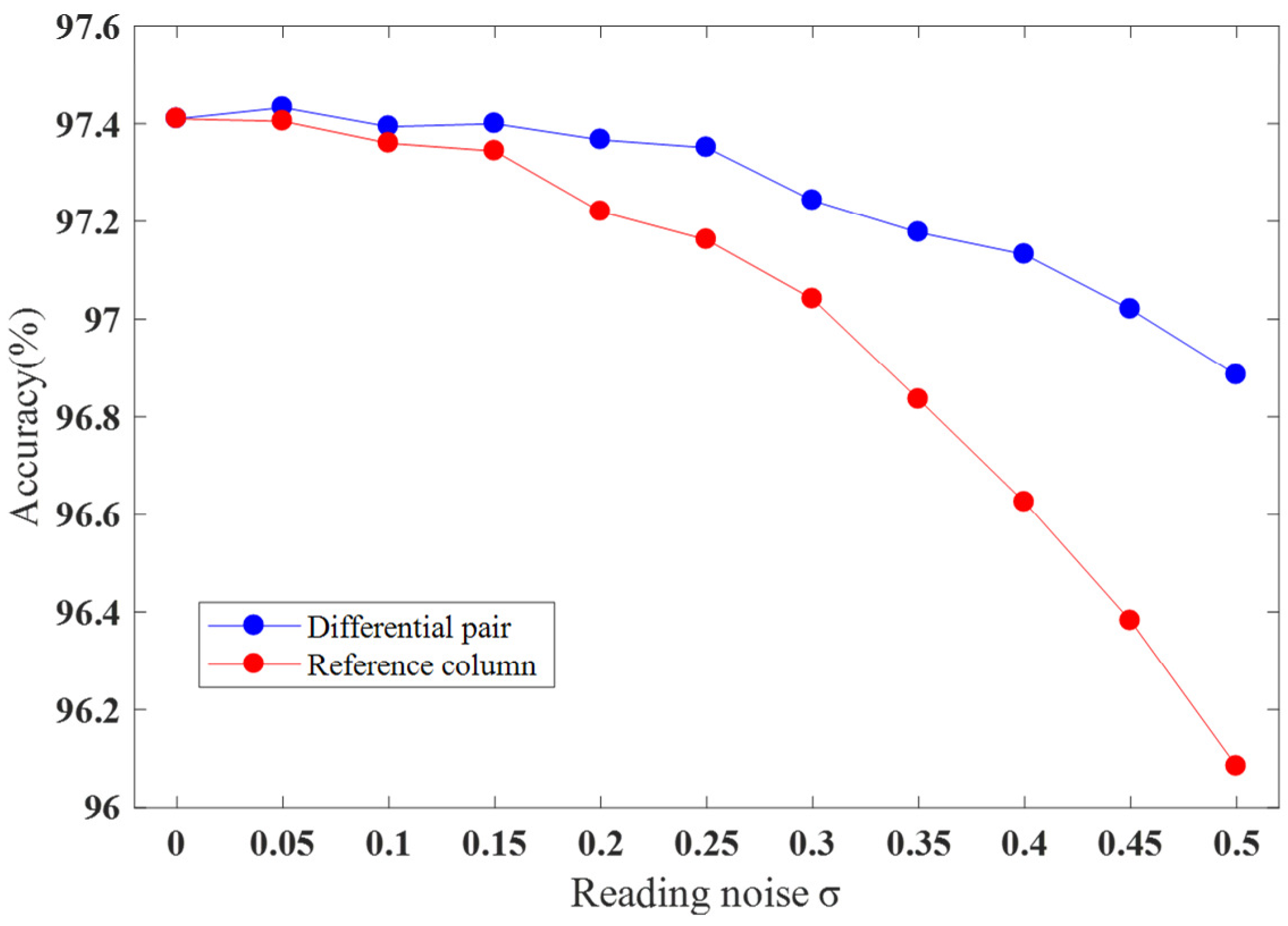
3.2.3. Reading Noise

Reading noise (thermal noise, 1/f noise and random telegraph noise, etc.) causes current read from memristor to be different from the true value [49,50,51]. Conductance changes between reading cycles due to noise follows a Gaussian distribution with a standard deviation of σ from the trained state of that memristor [49]. Figure 15 shows the effect of memristor volatility on MBNN with different schemes, and detailed values are given in Table 5.
It can be seen that recognition accuracy of both schemes decreases as reading noise increases. For the traditional structure, when σ is less than 0.45, recognition accuracy of MBNN is greater than 97%. Even if σ equals 0.5, recognition accuracy is still greater than 96.8%; for the proposed two-column reference scheme, when σ is smaller than 0.45, recognition accuracy of MBNN is greater than 97%; meanwhile, even if σ equals 0.5, recognition accuracy is still greater than 96.08%. When the level of reading noise is the same, the traditional differential pair structure has a greater recognition accuracy than the other one. Overall, the experimental results show that the two schemes have great robustness against reading noise, when σ is greater 0.5, a good recognition accuracy can be both achieved.

4. Experiment Environment and Configuration

In the training stage, the optimized algorithm of BNN were implemented using Theano framework, a Python library. Theano framework involves a large number of functions commonly used in deep learning, and it is efficient to calculate the gradient of neural network parameters. As for analysis of non-ideal factors, simulations were implemented by the C++ language. Both of them were implemented under the Windows 10 platform. The hardware platform included NVIDIA GeForce GTX1050Ti and Intel(R) Core (TM) i5-8300H CPU, 2.30 GHz, with 16 GB of memory. The computational time information of tasks completed under the Windows 10 platform is shown in Table 6 and Table 7 for readers to reference.
The hardware implementation simulated in Cadence Virtuoso version 17.0 environment was under the Linux platform. The processor of the hardware platform included two Intel Xeon Platinum 8124 M, 3.00 GHz, with 36 cores, 72 threads, 440 GB of memory, and Visual Studio Code was used to remote control the server. The computational time information of tasks completed under Linux platform is shown in Table 8.

5. Discussion

The ex situ training method is adopted in this work. That is, the weights trained in the software are mapped into the conductance of the crossbar array before the inference stage. Whereas, in the in situ training method, the weight value of each memristor devices has been updated after each iteration during training process in hardware. One of the major limitations of our work is that we do not include a training peripheral circuit in the MBNN implementation. However, the advantage of the ex situ method is that the optimization of the training algorithm is more convenient because there is no need to redesign the inference circuit, which is difficult in the in situ method.
Almost every topic related to the Internet of Things (IoT) systems refers to cloud computing and edge computing. Cloud is on the top level of data processing, which is responsible for large data processing. In contrast, edge computing means processing real-time data near the data source when the data are not sent to the cloud. Good scalability and low-energy consumption make the memristor circuit a promising solution for edge-computing devices, which means that the nanoscale edge-computing systems are application candidates for the proposed MBNN. There is no denying that BNNs show worse performance than analog networks on complex and heavy tasks because of low precision weights. Nevertheless, the recent research works show that the up-to-date memristive devices can achieve more than 64 stable resistive states [52]. This means that one of the major bottlenecks for memristive neural network is being removed. Hence, the proposed method of mapping weights is of great significance to the future hardware implementation for both binary and analog memristive neural networks.

6. Conclusions

In this work, we proposed a novel MBNN with a two-column reference structure that effectively solves the problem of sneak current effect and validated it by Cadence circuit simulation. Specifically, we made improvements to BNN algorithms and made it suitable for memristor array implementation. Compared to the traditional differential pair structure of MBNN, the proposed two-column reference scheme can reduce both the amount of memristors and the latency to refresh memristor array by nearly 50%. To further explore the robustness, memristor yield rate, fluctuation, and reading noise are considered. The experimental results demonstrate that when array yield α ≥ 5% or reading noise σ ≤ 0.25, a recognition accuracy greater than 97% in the MNIST data set is achieved. The experimental results manifest that the proposed scheme is robust to memristor array yield and reading noise, and slightly sensitive to memristor conductance fluctuation. To sum up, the proposed scheme provides a promising solution for on-chip circuit implementation of BNNs. After all, the MBNN designed and implemented in this work is a kind of fully connected structure. In future work, we will aim at exploring other memristive neural networks with more complex structures, such as convolutional neural network (CNN) and recurrent neural network (RNN), which need to further optimize the function and timing of the peripheral control circuit.

Author Contributions

Conceptualization, X.J.; Formal analysis, Y.Z.; Methodology, R.W.; Project administration, X.J.; Software, Y.W.; Validation, Y.W.; Writing—original draft, Y.Z.; Writing—review & editing, Y.R. All authors have read and agreed to the published version of the manuscript.

Funding

This work was supported in part by National Science Foundation of China under Grant 61072135, 81971702, the Fundamental Research Funds for the Central Universities under Grant 2042017gf0075, 2042019gf0072, and Natural Science Foundation of Hubei Province under Grant 2017CFB721.

Conflicts of Interest

The authors declare no conflict of interest.

Abbreviations

The following abbreviations are used in this manuscript:
BNNbinary neural network
CCVScurrent controlled voltage source
DNNsdeep neural networks
AIartificial intelligence
CPUCentral Processing Unit
GPUGraphic Processing Unit
FPGAField Programmable Gate Array
HPHewlett-Packard
RRAMresistive random access memory
CMOSComplementary Metal Oxide Semiconductor
MNISTMixed National Institute of Standards and Technology database
MBNNmemristive binary neural network
MOSFETMetal Oxide Semiconductor Field Effect Transistor
VMMvector-matrix multiplication
BNbatch normalization
MLPmulti-layer perceptron
HRShigh-resistance state
LRSlow-resistance state
CNNconvolutional neural network
RNNrecurrent neural network
IoTInternet of Things

References

  1. Klosowski, P. Deep Learning for Natural Language Processing and Language Modelling. In Proceedings of the 2018 Signal Processing: Algorithms, Architectures, Arrangements, and Applications (SPA), Poznan, Poland, 19–21 September 2018; pp. 223–228. [Google Scholar]
  2. Chen, L.C.; Papandreou, G.; Kokkinos, I.; Murphy, K.; Yuille, A.L. DeepLab: Semantic Image Segmentation with Deep Convolutional Nets, Atrous Convolution, and Fully Connected CRFs. IEEE Trans. Pattern Anal. Mach. Intell. 2018, 40, 834–848. [Google Scholar] [CrossRef]
  3. Komar, M.; Yakobchuk, P.; Golovko, V.; Dorosh, V.; Sachenko, A. Deep Neural Network for Image Recognition Based on the Caffe Framework. In Proceedings of the 2018 IEEE Second International Conference on Data Stream Mining & Processing (DSMP), Lviv, Ukraine, 21–25 August 2018; pp. 102–106. [Google Scholar]
  4. Ferlin, M.A.; Grochowski, M.; Kwasigroch, A.; Mikołajczyk, A.; Szurowska, E.; Grzywińska, M.; Sabisz, A. A Comprehensive Analysis of Deep Neural-Based Cerebral Microbleeds Detection System. Electronics 2021, 10, 2208. [Google Scholar] [CrossRef]
  5. Liu, F.; Ju, X.; Wang, N.; Wang, L.; Lee, W.J. Wind farm macro-siting optimization with insightful bi-criteria identification and relocation mechanism in genetic algorithm. Energy Convers. Manag. 2020, 217, 112964. [Google Scholar] [CrossRef]
  6. Park, K.; Lee, J.; Kim, Y. Deep Learning-Based Indoor Two-Dimensional Localization Scheme Using a Frequency-Modulated Continuous Wave Radar. Electronics 2021, 10, 2166. [Google Scholar] [CrossRef]
  7. Rashid, J.; Khan, I.; Ali, G.; Almotiri, S.H.; AlGhamdi, M.A.; Masood, K. Multi-Level Deep Learning Model for Potato Leaf Disease Recognition. Electronics 2021, 10, 2064. [Google Scholar] [CrossRef]
  8. Ortega-Zamorano, F.; Jerez, J.M.; Gómez, I.; Franco, L. Layer multiplexing FPGA implementation for deep back-propagation learning. Integr. Comput. Aided Eng. 2017, 24, 1–15. [Google Scholar] [CrossRef] [Green Version]
  9. Shawahna, A.; Sait, S.M.; El-Maleh, A. FPGA-based Accelerators of Deep Learning Networks for Learning and Classification: A Review. IEEE Access 2018, 7, 7823–7859. [Google Scholar] [CrossRef]
  10. Moore, G.E. Cramming More Components onto Integrated Circuits; Morgan Kaufmann Publishers Inc.: Burlington, MA, USA, 2000. [Google Scholar]
  11. Strukov, D.B.; Snider, G.S.; Stewart, D.R.; Williams, R.S. The missing memristor found. Nature 2008, 453, 80–83. [Google Scholar] [CrossRef]
  12. Xia, Q.; Robinett, W.; Cumbie, M.W.; Banerjee, N.; Cardinali, T.J.; Yang, J.J.; Wu, W.; Li, X.; Tong, W.M.; Strukov, D.B. Memristor-CMOS hybrid integrated circuits for reconfigurable logic. Nano Lett. 2009, 9, 3640. [Google Scholar] [CrossRef] [PubMed]
  13. Amirsoleimani, A.; Ahmadi, M.; Ahmadi, A. Logic Design on Mirrored Memristive Crossbars. IEEE Trans. Circ. Syst. II Express Briefs 2018, 65, 1688–1692. [Google Scholar] [CrossRef]
  14. Li, J.; Dong, Z.; Luo, L.; Duan, S.; Wang, L. A Novel Versatile Window Function for Memristor Model With Application in Spiking Neural Network. Neurocomputing 2020, 405, 239–246. [Google Scholar] [CrossRef]
  15. Duani, S.; Zhang, Y.; Hu, X.; Wang, L.; Li, C. Memristor-based chaotic neural networks for associative memory. Neural Comput. Appl. 2014, 25, 1437–1445. [Google Scholar] [CrossRef]
  16. Chen, P.Y.; Peng, X.; Yu, S. NeuroSim+: An integrated device-to-algorithm framework for benchmarking synaptic devices and array architectures. In Proceedings of the IEEE International Electron Devices Meeting, San Francisco, CA, USA, 7–11 December 2019. [Google Scholar]
  17. Xia, L.; Gu, P.; Li, B.; Tang, T.; Yin, X.; Huangfu, W.; Yu, S.; Cao, Y.; Wang, Y.; Yang, H. Technological Exploration of RRAM Crossbar Array for Matrix-Vector Multiplication. J. Comput. Sci. Technol. 2016, 31, 106–111. [Google Scholar] [CrossRef]
  18. Lee, M.K.F.; Cui, Y.; Somu, T.; Luo, T.; Zhou, J.; Tang, W.T.; Wong, W.-F.; Goh, R.S.M. A System-Level Simulator for RRAM-Based Neuromorphic Computing Chips. ACM Trans. Archit. Code Optim. 2019, 15, 1–24. [Google Scholar] [CrossRef] [Green Version]
  19. Song, J.A.; Sp, B.; Yu, W.A. A variation tolerant scheme for memristor crossbar based neural network designs via two-phase weight mapping and memristor programming. Future Gener. Comput. Syst. 2020, 106, 270–276. [Google Scholar]
  20. The MNIST Database of Handwritten Digits. Available online: http://yann.lecun.com/exdb/mni (accessed on 14 September 2021).
  21. Hasan, R.; Taha, T.M. Enabling back propagation training of memristor crossbar neuromorphic processors. In Proceedings of the 2014 International Joint Conference on Neural Networks (IJCNN), Beijing, China, 6–11 July 2014. [Google Scholar]
  22. Courbariaux, M.; Hubara, I.; Soudry, D.; El-Yaniv, R.; Bengio, Y. Binarized Neural Networks: Training Deep Neural Networks with Weights and Activations Constrained to +1 or −1. arXiv 2016, arXiv:1602.02830. [Google Scholar]
  23. Pi, S.; Li, C.; Jiang, H.; Xia, W.; Xin, H.L.; Yang, J.J.; Xia, Q. Memristor Crossbars with 4.5 Terabits-per-Inch-Square Density and Two Nanometer Dimension. arXiv 2018, arXiv:1804.09848. [Google Scholar]
  24. Choi, B.J.; Torrezan, A.C.; Strachan, J.P.; Kotula, P.G.; Lohn, A.J.; Marinella, M.J.; Li, Z.; Williams, R.S.; Yang, J.J. High-Speed and Low-Energy Nitride Memristors. Adv. Funct. Mater. 2016, 26, 5290–5296. [Google Scholar] [CrossRef] [Green Version]
  25. Yu, S.; Li, Z.; Chen, P.Y.; Wu, H.; He, Q. Binary neural network with 16 Mb RRAM macro chip for classification and online training. In Proceedings of the 2016 IEEE International Electron Devices Meeting (IEDM), San Francisco, CA, USA, 3–7 December 2016. [Google Scholar]
  26. Hirtzlin, T.; Bocquet, M.; Penkovsky, B.; Klein, J.O.; Nowak, E.; Vianello, E.; Portal, J.M.; Querlioz, D. Digital Biologically Plausible Implementation of Binarized Neural Networks with Differential Hafnium Oxide Resistive Memory Arrays. Front. Neurosci. 2019, 13, 1383. [Google Scholar] [CrossRef] [Green Version]
  27. Pham, K.V.; Nguyen, T.V.; Tran, S.B.; Nam, H.K.; Mi, J.L.; Choi, B.J.; Truong, S.N.; Min, K.S. Memristor Binarized Neural Networks. J. Semicond. Technol. Sci. 2018, 18, 568–588. [Google Scholar] [CrossRef]
  28. Truong, S.N.; Min, K.S. New Memristor-Based Crossbar Array Architecture with 50% Area Reduction and 48% Power Saving for Matrix-Vector Multiplication of Analog Neuromorphic Computing. J. Semiconduct. Technol. Sci. 2014, 14, 356–363. [Google Scholar] [CrossRef] [Green Version]
  29. Qin, Y.F.; Kuang, R.; Huang, X.D.; Li, Y.; Chen, J.; Miao, X.S. Design of High Robustness BNN Inference Accelerator Based on Binary Memristors. IEEE Trans. Electron. Dev. 2020, 67, 3435–3441. [Google Scholar] [CrossRef]
  30. Gardner, M.W. Artificial neural networks (the multilayer perceptron)—A review of applications in the atmospheric sciences. Atmos. Environ. 1998, 32, 2627–2636. [Google Scholar] [CrossRef]
  31. Pershin, Y.V.; Ventra, M. SPICE model of memristive devices with threshold. Radioengineering 2013, 22, 485–489. [Google Scholar]
  32. Ranjan, R.; Ponce, P.M.; Hellweg, W.L.; Kyrmanidis, A.; Saleh, L.A.; Schroeder, D.; Krautschneider, W.H. Integrated Circuit with Memristor Emulator Array and Neuron Circuits for Biologically Inspired Neuromorphic Pattern Recognition. J. Circ. Syst. Comput. 2017, 26, 1750183. [Google Scholar] [CrossRef] [Green Version]
  33. Cheng, L.; Li, Y.; Yin, K.; Hu, S.; Miao, X. Functional Demonstration of a Memristive Arithmetic Logic Unit (MemALU) for In-Memory Computing. Adv. Funct. Mater. 2019, 29, 1905660. [Google Scholar] [CrossRef]
  34. Liang, Y.; Lu, Z.; Wang, G.; Yu, D.; Iu, H.C. Threshold-type Binary Memristor Emulator Circuit. IEEE Access 2019, 7, 180181–180193. [Google Scholar] [CrossRef]
  35. Shukla, A.; Prasad, S.; Lashkare, S.; Ganguly, U. A case for multiple and parallel RRAMs as synaptic model for training SNNs. In Proceedings of the 2018 International Joint Conference on Neural Networks (IJCNN), Rio de Janeiro, Brazil, 8–13 July 2018. [Google Scholar]
  36. Sangwan, V.K.; Lee, H.S.; Bergeron, H.; Balla, I.; Beck, M.E.; Chen, K.S.; Hersam, M.C. Multi-Terminal Memtransistors from Polycrystalline Monolayer MoS2. Nature 2018, 554, 500–504. [Google Scholar] [CrossRef]
  37. Luo, S.; Liao, K.; Lei, P.; Jiang, T.; Hao, J. Synaptic memristor based on two-dimensional layered WSe2 nanosheets with short- and long-term plasticity. Nanoscale 2021, 13, 6654–6660. [Google Scholar] [CrossRef]
  38. Zhang, W.; Gao, H.; Deng, C.; Lv, T.; Hu, S.; Wu, H.; Xue, S.; Tao, Y.; Deng, L.; Xiong, W. An ultrathin memristor based on a two-dimensional WS2/MoS2 heterojunction. Nanoscale 2021, 13, 11497–11504. [Google Scholar] [CrossRef] [PubMed]
  39. Bala, A.; Adeyemo, A.; Yang, X.; Jabir, A. Learning method for ex-situ training of memristor crossbar based multi-layer neural network. In Proceedings of the 2017 9th International Congress on Ultra Modern Telecommunications and Control Systems and Workshops (ICUMT), Munich, Germany, 6–8 November 2017. [Google Scholar]
  40. Hasan, R.; Taha, T.M.; Yakopcic, C. On-chip training of memristor crossbar based multi-layer neural networks. Microelectron. J. 2017, 66, 31–40. [Google Scholar] [CrossRef]
  41. Zhou, Z.; Huang, P.; Xiang, Y.C.; Shen, W.S.; Kang, J.F. A new hardware implementation approach of BNNs based on nonlinear 2T2R synaptic cell. In Proceedings of the 2018 IEEE International Electron Devices Meeting (IEDM), San Francisco, CA, USA, 10–18 December 2020. [Google Scholar]
  42. Prezioso, M.; Merrikh-Bayat, F.; Hoskins, B.D.; Adam, G.C.; Likharev, K.K.; Strukov, D.B. Training and operation of an integrated neuromorphic network based on metal-oxide memristors. Nature 2015, 521, 61–64. [Google Scholar] [CrossRef] [Green Version]
  43. Jung, C.M.; Choi, J.M.; Min, K.S. Two-Step Write Scheme for Reducing Sneak-Path Leakage in Complementary Memristor Array. IEEE Trans. Nanotechnol. 2012, 11, 611–618. [Google Scholar] [CrossRef]
  44. Cong, X.; Niu, D.; Muralimanohar, N.; Balasubramonian, R.; Yuan, X. Overcoming the challenges of crossbar resistive memory architectures. In Proceedings of the IEEE International Symposium on High Performance Computer Architecture, Burlingame, CA, USA, 7–11 February 2015. [Google Scholar]
  45. Frey, P.; O’Riordan, D. Verilog-AMS: Mixed-Signal Simulation and Cross Domain Connect Modules. In Proceedings of the 2000 IEEE/ACM International Workshop on Behavioral Modeling and Simulation, Orlando, FL, USA, 18–20 October 2000; p. 103. [Google Scholar]
  46. Bidmeshki, M.M.; Antonopoulos, A.; Makris, Y. Proof-Carrying Hardware-Based Information Flow Tracking in Analog/Mixed-Signal Designs. IEEE J. Emerg. Sel. Top. Circuits Syst. 2021, 11, 415–427. [Google Scholar] [CrossRef]
  47. Liu, C.; Hu, M.; Strachan, J.P.; Li, H. Rescuing Memristor-based Neuromorphic Design with High Defects. In Proceedings of the Design Automation Conference, Austin, TX, USA, 18–22 June 2017; pp. 1–6. [Google Scholar]
  48. Xu, N.; Liang, F.; Chi, Y.; Chao, Z.; Tang, Z. Resistance uniformity of TiO2 memristor with different thin film thickness. In Proceedings of the 2014 IEEE 14th International Conference on Nanotechnology (IEEE-NANO), Toronto, ON, Canada, 18–21 August 2014. [Google Scholar]
  49. Veksler, D.; Bersuker, G.; Vandelli, L.; Padovani, A.; Larcher, L.; Muraviev, A.; Chakrabarti, B.; Vogel, E.; Gilmer, D.C.; Kirsch, P.D. Random telegraph noise (RTN) in scaled RRAM devices. In Proceedings of the 2013 IEEE International Reliability Physics Symposium, Monterey, CA, USA, 14–18 April 2013; pp. MY.10.1–MY.10.4. [Google Scholar]
  50. Agarwal, S.; Plimpton, S.J.; Hughart, D.R.; Hsia, A.H.; Marinella, M.J. Resistive memory device requirements for a neural algorithm accelerator. In Proceedings of the International Joint Conference on Neural Networks, Vancouver, BC, Canada, 24–29 July 2016; pp. 929–938. [Google Scholar]
  51. Ambrogio, S.; Balatti, S.; Mccaffrey, V.; Wang, D.C.; Ielmini, D. Noise-Induced Resistance Broadening in Resistive Switching Memory—Part II: Array Statistics. IEEE Trans. Electron. Dev. 2015, 62, 3812–3819. [Google Scholar] [CrossRef]
  52. Li, C.; Hu, M.; Li, Y.; Jiang, H.; Ge, N.; Montgomery, E.; Zhang, J.; Song, W.; Dávila, N.; Graves, C.E.; et al. Analogue signal and image processing with large memristor crossbars. Nat. Electron. 2018, 1, 52–59. [Google Scholar] [CrossRef]
Figure 1. Schematic of BNN algorithms.
Electronics 10 02600 g001
Figure 2. Inference accuracy of cropped MNIST handwritten digits data set of different topologies.
Electronics 10 02600 g002
Figure 3. The I-V characteristic curve of memristor model simulated by Verilog-AMS.
Electronics 10 02600 g003
Figure 4. Memristor conductance modulated by voltage pulses.
Electronics 10 02600 g004
Figure 5. VMM implemented by memristor array.
Electronics 10 02600 g005
Figure 6. The schematic of memristive array structures to implement MBNN: (a) Traditional differential pair structure. (b) The select column scheme. Memristors in the select column are turned into G L R S , and the current mirror converts Isel to the half of itself [27]. (c) The proposed two-column reference memristor scheme. Memristors in the first reference column are turned into G H R S , and memristors in the second reference column are turned into G L R S .
Electronics 10 02600 g006
Figure 7. Voltage bias scheme in writing operation of memristive crossbar array: (a) SET LRS, (b) SET HRS.
Electronics 10 02600 g007
Figure 8. The voltage signals of output neurons in MBNN based on the differential pair structure.
Electronics 10 02600 g008
Figure 9. The voltage signals of output neurons in MBNN based on the two-column reference structure.
Electronics 10 02600 g009
Figure 10. Schematic diagram of MBNN structure to study non-deal effects.
Electronics 10 02600 g010
Figure 11. Schematic diagram of yield model of a m × n memristor array.
Electronics 10 02600 g011
Figure 12. The recognition accuracy of the two schemes during the test, the x-axis represents memristor device yield.
Electronics 10 02600 g012
Figure 13. Schematic diagram of fluctuation model of m × n memristor array.
Electronics 10 02600 g013
Figure 14. The recognition accuracy of the two schemes, the x-axis represents device fluctuation.
Electronics 10 02600 g014
Figure 15. The recognition accuracy of the two schemes, the x-axis represents the level of reading noise.
Electronics 10 02600 g015
Table 1. The recognition accuracy of BNNs of different topologies.
Number of Hidden Neurons Per Layer1 Hidden Layer2 Hidden Layers3 Hidden Layers
10091.8%91.83%92.3%
40095.89%97.1%97.15%
70096.88%97.82%98.05%
100097.41%97.99%98.36%
130097.58%98.3%98.31%
160097.78%98.25%98.27%
190097.74%98.45%98.4%
220097.88%98.36%98.35%
Table 2. Comparison between two structures to implement MBNNs.
400 × 100 × 10 MBNNThe Traditional Differential StructureThe Proposed Two-Column Reference Structure
Total number of memristors82,00042,000
Writing time40 µs20.4 µs
Recognition accuracy91.8%91.8%
Table 3. The recognition accuracy of the two schemes at different levels of memristor device yield.
Device Yield RateThe Traditional Differential StructureThe Proposed Two-Column Reference Structure
100%97.41%97.41%
99%97.4%97.28%
98%97.37%97.33%
97%97.3%97.26%
96%97.26%97.12%
95%97.17%97.04%
94%97.23%97.11%
93%97.26%96.97%
92%97.08%96.98%
91%96.99%96.77%
90%96.98%96.89%
Table 4. The recognition accuracy of the two schemes at different levels of memristor device fluctuation.
Device Fluctuation σ The Traditional Differential StructureThe Proposed Two-Column Reference Structure
097.41%97.41%
0.0597.407%94.153%
0.197.383%91.49%
0.1597.209%89.69%
0.297.166%90.529%
0.2596.972%87.598%
0.396.968%86.593%
0.3596.068%85.85%
0.496.313%83.982%
0.4592.173%79.486%
0.589.983%76.919%
Table 5. The recognition accuracy of the two schemes at different levels of reading noise.
Reading Noise σ The Traditional Differential StructureThe Proposed Two-Column Reference Structure
097.41%97.41%
0.0597.47%97.42%
0.197.32%97.46%
0.1597.39%97.4%
0.297.25%97.27%
0.2597.3%97.25%
0.397.25%96.98%
0.3597.18%96.75%
0.497.09%96.63%
0.4597.09%96.27%
0.596.77%96.05%
Table 6. Computational time of C++ language under the Windows 10 platform.
Analysis of Non-Ideal FactorsThe Traditional Differential StructureThe Proposed Two-Column Reference Structure
400 × 1000 × 10 MBNN (Device yield rate)62 min20 min
400 × 1000 × 10 MBNN (Device fluctuation)58 min21 min
400 × 1000 × 10 MBNN (Reading noise)60 min20 min
Table 7. Computational time of the Python language under the Windows 10 platform.
Training StageThe Traditional Differential StructureThe Proposed Two-Column Reference Structure
400 × 100 × 10 MBNN10 h10 h
400 × 1000 × 10 MBNN3 h3 h
Table 8. Computational time of Verilog-AMS language under the Linux platform.
Inference StageThe Traditional Differential StructureThe Proposed Two-Column Reference Structure
400 × 100 × 10 MBNN47 h18 h
Publisher’s Note: MDPI stays neutral with regard to jurisdictional claims in published maps and institutional affiliations.

