Abstract
This paper proposes an AC/DC single-stage structure by integrating a boost topology and an active clamp flyback (ACF) circuit with power-factor-correction (PFC) function. The PFC function can be achieved by controlling a boost PFC topology operated in the discontinuous conduction mode. With the coordination of active clamping components, a resonant technique is obtained and zero-voltage-switching (ZVS) can be achieved. The proposed converter is combined with the advantages of: (1) compared with two-stage circuit, a single stage circuit decreases the component of the main circuit and reduces the complexity of the control circuit; (2) a boost topology with PFC function operated in discontinuous conduction mode can be accomplished without adding any current detecting technique or detecting input signal; (3) by using the inductor from the PFC stage, ZVS function can be achieved without any additional inductor; (4) the increment of switching frequency facilitates the optimization of power density; (5) the conducting loss at the secondary side can be reduced by adding the synchronous rectification; (6) in this proposed scheme, the dual transformers with series-parallel connection are utilized, the current at the secondary side can be shared for lowering the conduction loss of the synchronous transistors. Finally, a prototype converter with AC 110 V input and DC 19 V/6.32 A (120 W) output under 300 kHz switching frequency is implemented. The efficiency of the proposed converter reaches 88.20% and 0.984 power factor in full load condition.
1. Introduction
The development of civilization and the rapid advancement of science and technology have led to a shortage of our energy. The optimization of efficiency has become one of the main goals in power electronic industries; thus, many countries have begun to establish different kinds of standards for energies gradually. In addition to that, the dimension, the efficiency, and the power density of power supplies are much more a matter of concern today. Therefore, various topologies and control methods are proposed to improve the aforementioned issues widely.
Flyback converters [1,2,3] are the most commonly used in low power electronics applications and consumer products, such as smart phone chargers, adaptors for laptops, and electric scooter battery chargers. The active-clamp techniques [4,5,6,7] have improved several drawbacks of the conventional flyback converter topology. The additional clamping capacitor can absorb the energy which is stored in the leakage inductor [8]. This helps to reduce voltage spikes during switching conditions [9,10]. By designing the parameters of the leakage inductor and the clamping capacitor to resonate appropriately, ZVS can be achieved easily [11]. This technique not only releases the energy of leakage inductance efficiently, but also makes good use of it by achieving soft switching to reduce switching loss. To pursue higher power density, increasing switching frequency can reduce the size of the transformer and magnetic component. Thus, the soft switching technique is one of the common ways to increase the switching frequency and the efficiency to a higher level. The synchronous rectification (SR) technique is also a trend to improve the efficiency of converters currently. The SR switch can be controlled by detecting the voltage across the SR switch at the secondary side. The switching period can be controlled appropriately. However, if the SR technique works perfectly and precisely, proper layout of the schematic and the good driving signal are necessary.
In addition to the better performance of converters’ efficiency, the power factor (PF) is also a key index to describe the ratio of real power and apparent power. Different output load characteristics will cause the phase shift and deformation of the input current waveform. The increment of the reactive power from the AC main will increase the losses of power line during the energy delivering process. Thus, the PFC technique [12,13] is widely used to maintain the level of power factor and to fulfill the electrical specifications of power supplies. It can be classified into passive and active [14,15,16] methods. The passive method is mainly realized by passive components which has a low cost but large size. The effect of power factor correction is also limited; active methods use the additional switch and circuit to make the input current and voltage waveform in phase to improve power factor. By using this technique, PF can approach 1 with low harmonic. The effect of the active method is much better than that of the passive one, but this method requires one independent circuit with control stage to achieve. That requires more components and the cost will also increase
In general, the structure of AC-DC converter with PFC function is a two-stage topology. It can be divided by two independent circuits [17,18]. Both of the independent circuits need to be operated by their own control systems. Hence, the number of components will definitely be increased. In order to simplify the structure of the two-stage circuit [19,20], the single-stage architecture was proposed.
In reference [21], a boost converter and a flyback converter with valley switching were combined. With the valley switching technique, switching loss is reduced by detecting auxiliary winding. The secondary side synchronous rectification is achieved through the self-made detection mechanism for increasing overall efficiency. However, it is difficult for the power factor to exceed 0.9, and the voltage spike problem of VDS is the obstacle for developing toward a higher frequency level. Reference [22] combined a boost converter with a low-side ACF converter. Soft switching can be used to increase the switching frequency and efficiency. P-channel MOSFET can be utilized to solve the isolation issue for high-side switch in ACF topology. However, it is not common for P-channel MOSFET to have a high withstanding voltage in practical. An external inductor is also needed to achieve ZVS which increases the elements of the circuit. In reference [23], an interleaved PFC boost converter is proposed and the efficiency goes to 95% under 110 V AC input. Reference [24] proposed an ACF converter with 93% of efficiency under 120 W output condition. The overall efficiency reached about 88.35% if the ACF and PFC stages were connected. Reference [25] proposed integrating a bridgeless boost and a LLC converter. ZVS and ZCS are achieved under different conditions, but several diodes are required to prevent the wrong current direction. Thus, an external inductor is also needed in the LLC resonant tank of the circuit. It also increases the total component of the circuit. In [26], a novel high-gain DC-DC boost converter with lower component count was implemented. This novel boost converter has higher power density characteristics which is suitable for the smaller size of electronic product with PFC function to boost the voltage for 400 Vdc applications. Lower component counts also bring lower cost and loss.
To compare with previous studies, several papers have proposed a single-stage PFC converter with soft-switching technique. From [26,27,28,29], they provided different kinds of single-stage structures, and they have different benefits and features individually. In reference [27], the number of switches is one, thus the switching loss is low. In reference [28,29], the number of switches is two. The switching losses are still low, but the performances of THD for these three references are moderate or even higher. For the proposed circuit, two of the switches are used for PFC and ACF functions, the other two switchers are used for synchronous rectification for decreasing the conduction loss, and THD performs well among these studies. Table 1 shows a comparison of the related studies.

Table 1.
Comparison of the related single-stage converter with soft-switching function.
To combine with the PFC stage and the DC-DC converter into one simple circuit is the main concept of this paper. It not only reduces the number of components, but also delivers the energy to the output load directly. The proposed paper is to combine the PFC technique and ACF converter into the single-stage structure. The goal of this paper is to simplify the structure and also to implement the single-stage PFC and ACF converter with dual transformer. In this proposed circuit, the dual transformers with series input and parallel output connection were selected. The benefit of this connection is that each of the transformers only needs to deliver half of the power from input to the output load. The larger inductance causes smaller current variation on Lm. This situation can reduce the peak value and effective value of the primary side current. To compare with the volume of a single winding transformer, the dual transformers are indeed larger than the single one. However, the diameter of copper wire and the size of magnetic core can be smaller for dual transformer topology. In addition, the synchronous mechanism can reduce the conduction loss effectively. To sum up the characteristics and the functions above, the proposed topology is suitable for higher power demand adaptor applications, such as gaming laptops and mini-computers.
2. Proposed AC-DC Converter
2.1. The Proposed Circuit Structure
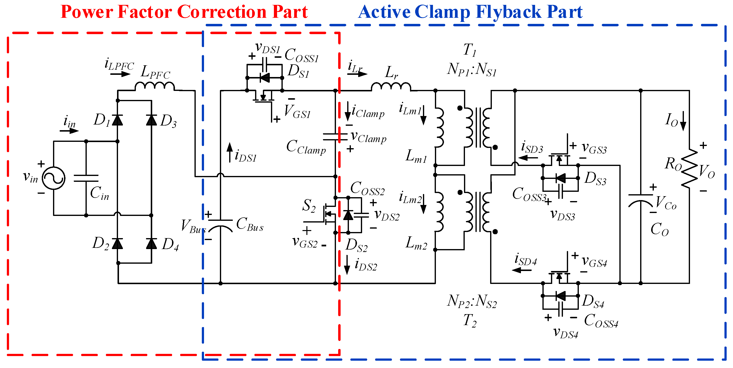
In this paper, a single-stage circuit with AC input and DC output was developed as shown in Figure 1. The proposed design utilizes a PFC boost topology to combine with the active clamp flyback converter without any external resonant inductor [9]. The clamping capacitor CClamp can be shared as the common current path for both stages to reduce the number of main circuit components. The PFC stage is operated under discontinuous conduction mode for full range to lower the complexity of the PFC control method. Due to the characteristics of active clamping technique, ZVS can be easily achieved on both switches S1 and S2 at the primary side. In addition to that, the dual transformer connection and the synchronous rectification technique at the secondary side can reduce the conduction loss effectively.

Figure 1.
Topology of the proposed circuit.
2.2. Principle of Operation
Since the AC input voltage passes through a full-bridge rectifier, no matter whether the input voltage is positive or negative, the output voltage of the rectifier is still positive. Therefore, the following description will only focus on the positive waveform duration. As shown in Figure 2, due to the topology of the circuit, the sinusoidal waveform changes as the value of changes. The waveform can be divided into the valley, the middle, and the peak point. The valley point means that the rectified voltage drops to 0 V and this valley point is operated as a conventional active clamp flyback converter. The peak points are influenced by the value of the most. For the time axis, and are the peak points of the rectified voltage. The middle points are located between the valley and the peak points which are at and of the time axis.
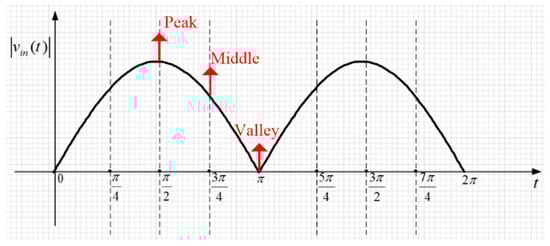
Figure 2.
Output voltage from the rectifier circuit.
After the definition of these critical points, the operation modes of the circuit will be discussed in this section. The current path of the primary side and the secondary side will be illustrated in different colors. The blue shows the power factor correction path. The red shows the active clamp current path. The green shows the current at the secondary side. These current paths help to simplify the following explanation, and the theoretical paths are shown in Figure 3.
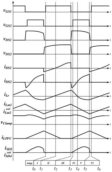
Figure 3.
The related key waveforms of the proposed circuit.
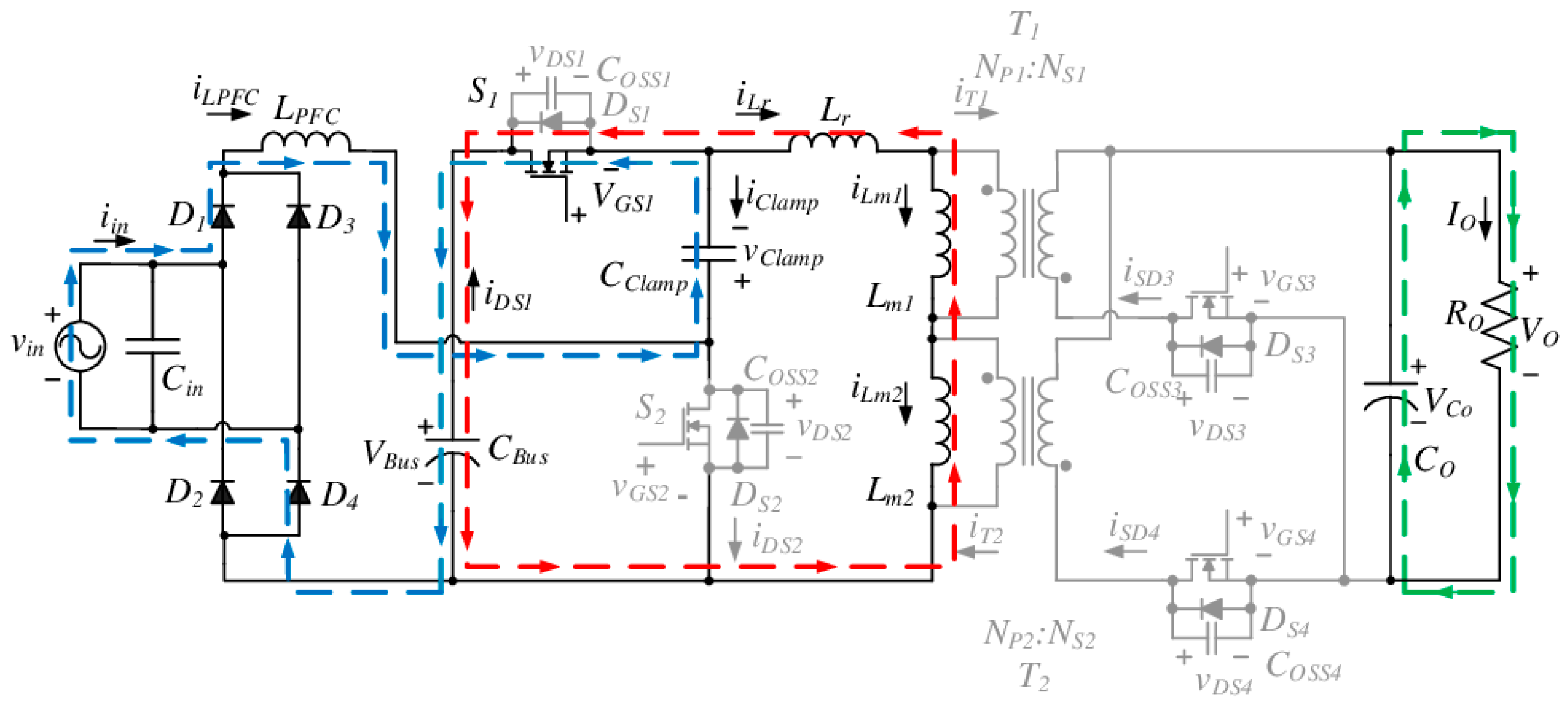
2.2.1. Mode 1—(t0 < t < t1)
As shown in Figure 4, due to the previous mode, the high side switch’s parasitic capacitor COSS1 is discharged to zero and then S1 turns on in this mode. ZVS of S1 can be achieved. At the beginning of this mode, the total leakage inductor Lr, the magnetic inductors Lm1 and Lm2 keep the same current direction and charge to CBus as the previous state. The energy stored in the power factor correction inductor LPFC also charges to the capacitor CBus at the same time. When the energy stored in Lr, Lm1, and Lm2 are released, the current direction of these inductors turns to be positive and starts to be charged. When the charging process of CBus ends, the coming operation mode will be carried out. In this mode, there is no energy delivered to the secondary side. The switches S3 and S4 at the secondary side are turned off; hence, the energy of the output load RO is provided by the output capacitor Co. Through the analysis above, Equations (1) and (2) can be obtained below. ω1 is the angular frequency of the AC input voltage. In this mode, the angular frequency ω and the impedance Z are also shown in Equation (3).
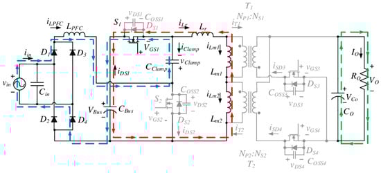
Figure 4.
Current route of Mode 1.
2.2.2. Mode 2—(t1 < t < t2)
As shown in Figure 5, in this mode, S1 still turns on. LPFC continues releasing the energy and charging to the clamping capacitor CClamp from mode 1. LPFC also charges to Lr, Lm1, and Lm2. In the meantime, CBus also charges to Lr, Lm1, and Lm2 through S1. When the energy of LPFC is exhausted, iLPFC drops to 0 A. Thus, VClamp starts to be clamped at a constant voltage temporarily. This mode ends when S1 is turned off.
Figure 5.
Current route of Mode 2.
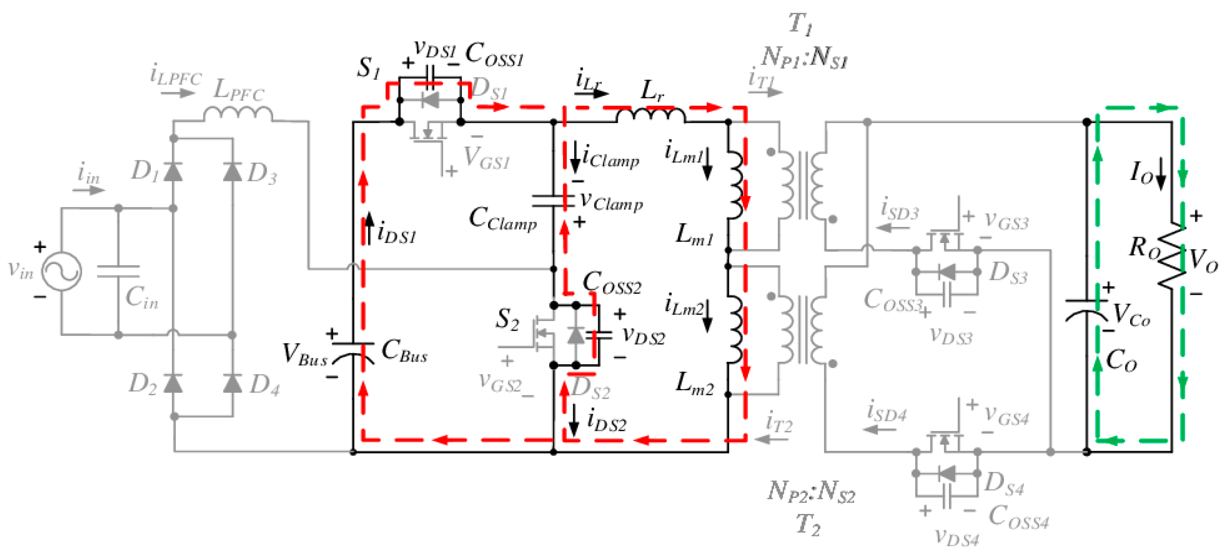
2.2.3. Mode 3—(t2 < t < t3)
As shown in Figure 6, during the dead time, COSS1 is charged by the path of CBus. The charging path will be open when COSS1 is charged to the sum of VBus and vClamp. Since Lr, Lm1, and Lm2 maintain the same current direction from the previous step, the energy on COSS2 will be taken away while the current goes through S2. After COSS2’s energy releases to zero, S2’s body diode DS2 will be turned on to maintain the negative current path. This mode ends when dead time is finished. In this step, no energy is transmitted to the secondary side. The secondary side switches S3 and S4 are turned off, the energy of the output load RO is provided by the output capacitor Co. Equation (4) can be analyzed through this step; ω and Z’s equation are shown in (5).
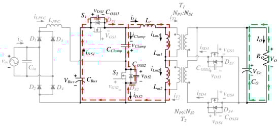
Figure 6.
Current route of Mode 3.
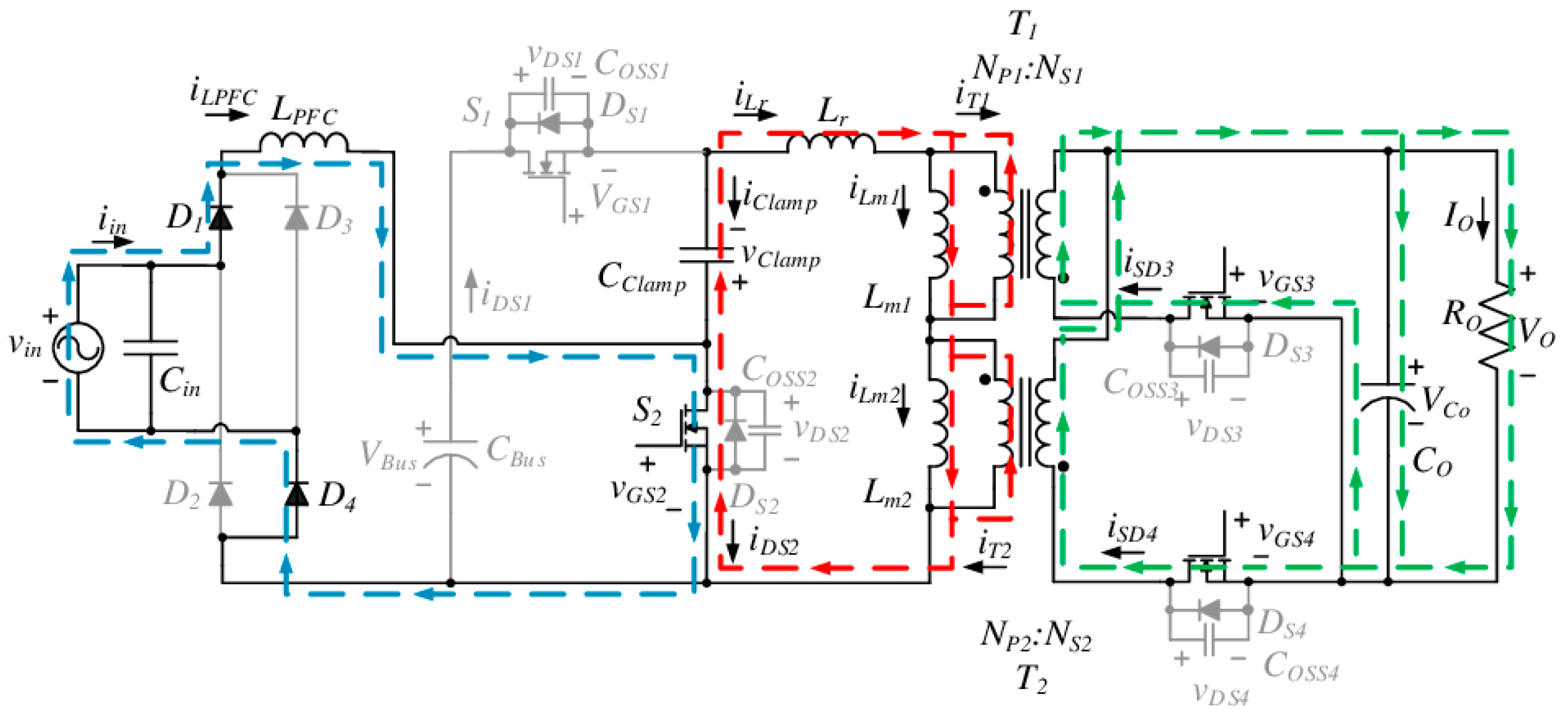
2.2.4. Mode 4—(t3 < t < t4)
As shown in Figure 7, due to the previous mode, the low side switch’s capacitor COSS2 is released to zero during the switching of S2 in this mode. S2’s ZVS can be achieved. LPFC will be charged by input AC power. Lr and CClamp start to resonate with each other, the next mode begins when Lr releases its energy to zero. The magnetizing inductors Lm1 and Lm2 transfer energy to secondary side, vGS3 and vGS4 turn high to achieve synchronous rectification function to reduce losses of S3 and S4. Equations (6) and (7) can be analyzed through this step; ω and Z’s equation are shown in (8).
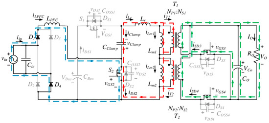
Figure 7.
Current route of Mode 4.
2.2.5. Mode 5—(t4 < t < t5)
As shown in Figure 8, due to the exhaustion of Lr, CClamp releases its energy to Lr. Both components keep resonating with the opposite current direction as shown in mode 4. Lm1 and Lm2 release their energy to secondary side at the beginning of this step. When both of the magnetizing inductors release to zero, CClamp will transfer its energy to Lm1, Lm2, and the secondary side. The current direction of iLm1 and iLm2 will be opposite to the beginning of this step. Lm1 and Lm2 transfer energy to secondary at the beginning of this step, CClamp will keep transferring when the magnetizing inductors are out of energy. vGS3 and vGS4 remain high to achieve synchronous rectification function for reducing losses of S3 and S4. Equations (9) and (10) can be analyzed through this step; ω and Z’s equation are shown in (11).
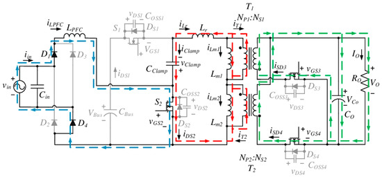
Figure 8.
Current route of Mode 5.
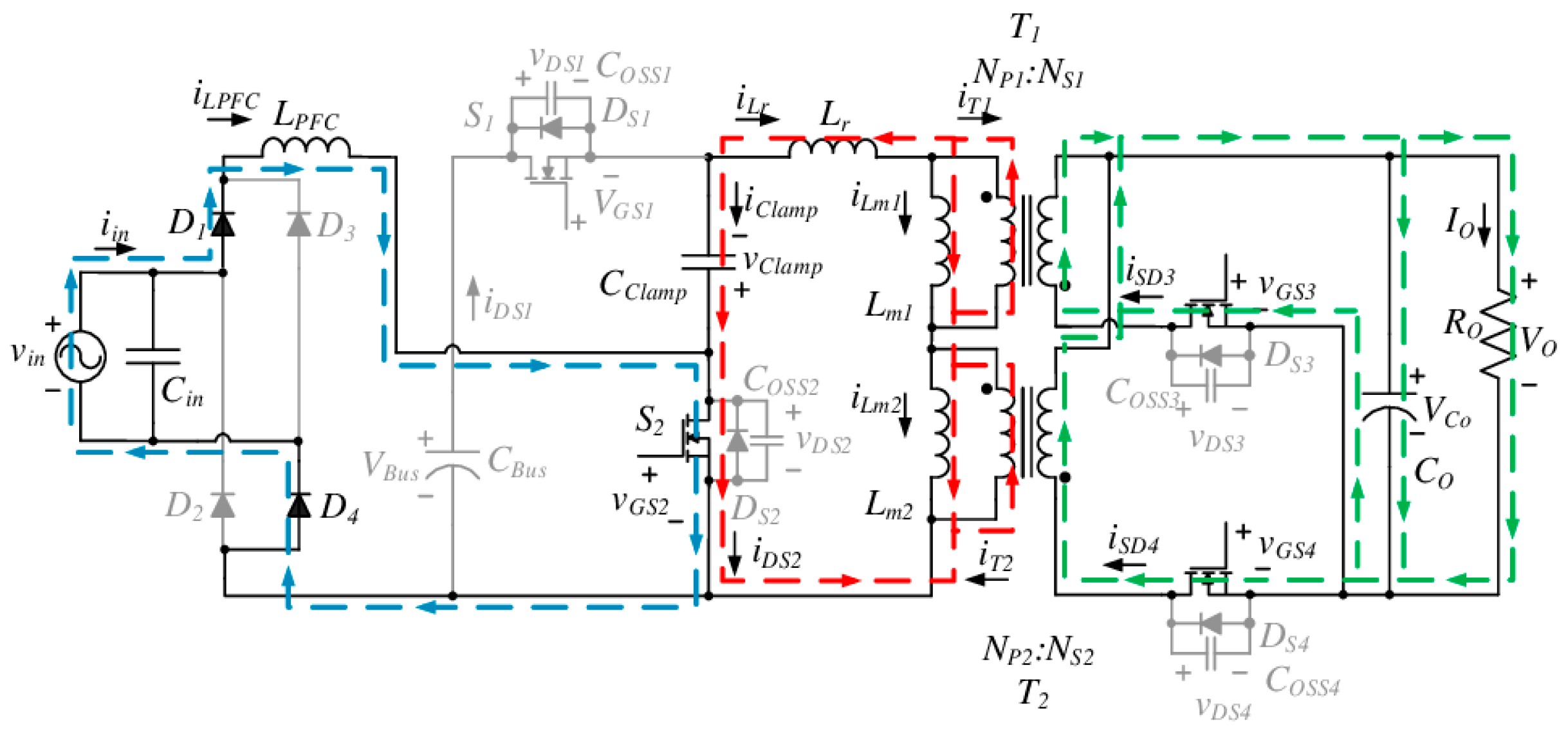
2.2.6. Mode 6—(t5 < t < t6)
As shown in Figure 9, during the dead time, COSS2 starts to be charged. The charging path is open when COSS2 is charged to the sum of VBus and vClamp. Since Lr, Lm1, and Lm2 maintain the same current direction from the previous step, the energy on COSS1 will be taken away during the current went through S1. After COSS1’s energy releases to zero, S2’s body diode DS2 is turned on to maintain the negative current path. In this mode, LPFC starts to discharge and to release energy to CClamp, CBus, and COSS2. COSS1 also discharges at the same time. This mode ends when dead time is finished. CClamp keeps transferring energy to secondary side. vGS3 and vGS4 remain high to achieve synchronous rectification function. Equation (12) can be analyzed through this step; ω and Z’s equation are shown in Equation (13).
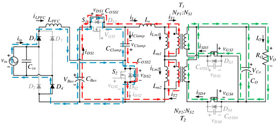
Figure 9.
Current route of Mode 6.
2.3. Design Consideration
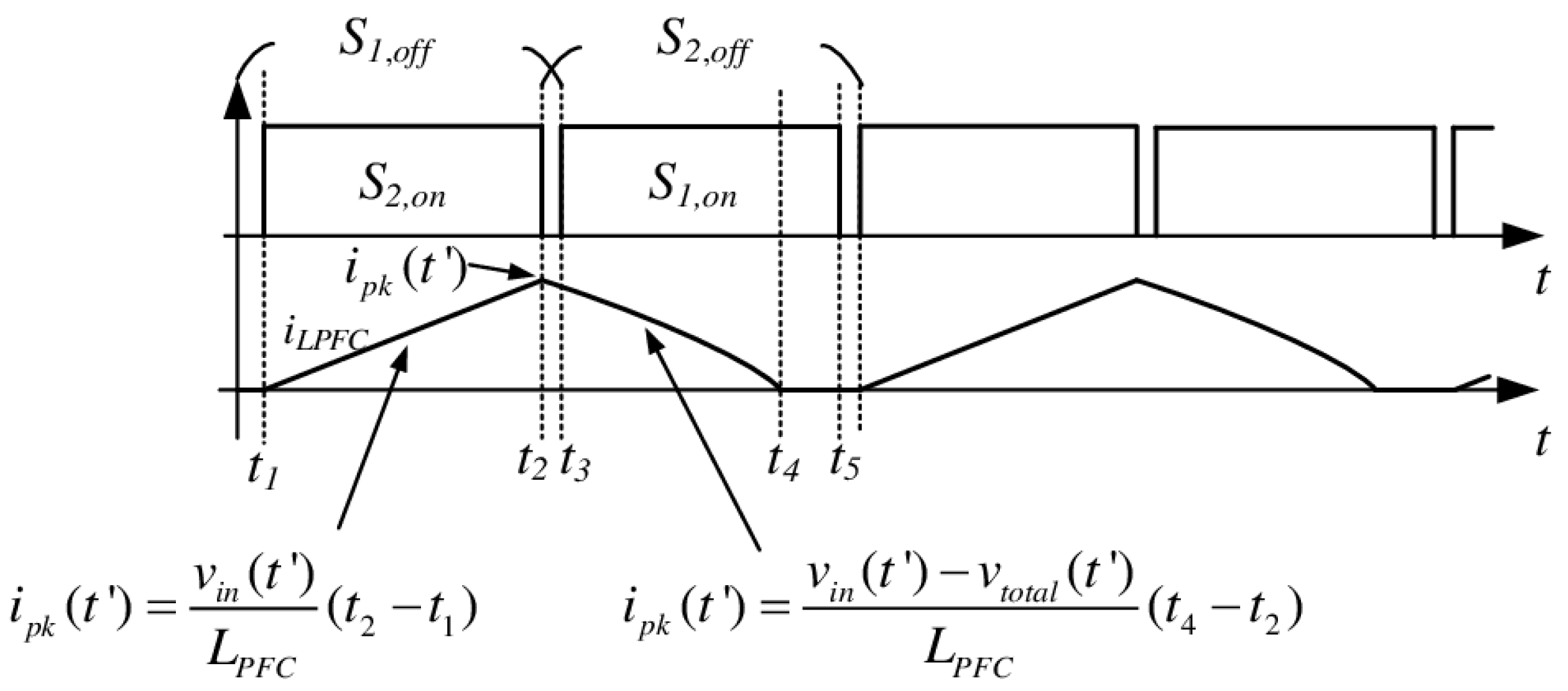
In order to simplify the design of single-stage architecture, the power factor correction inductor is designed to operate under discontinuous conduction mode [10,11]. The extra input voltage or current signal detection mechanism for continuous conduction mode or boundary conduction mode [12,13] can be removed. In the case of discontinuous conduction mode, Figure 10 can be drawn. The relationship of iLPFC during the on and off time of the power switch can be obtained through the operation process, where vtotal(t’) represents VBus + vClamp(t’).
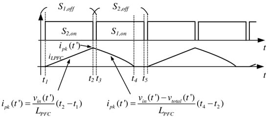
Figure 10.
The waveform of iLPFC and switches.
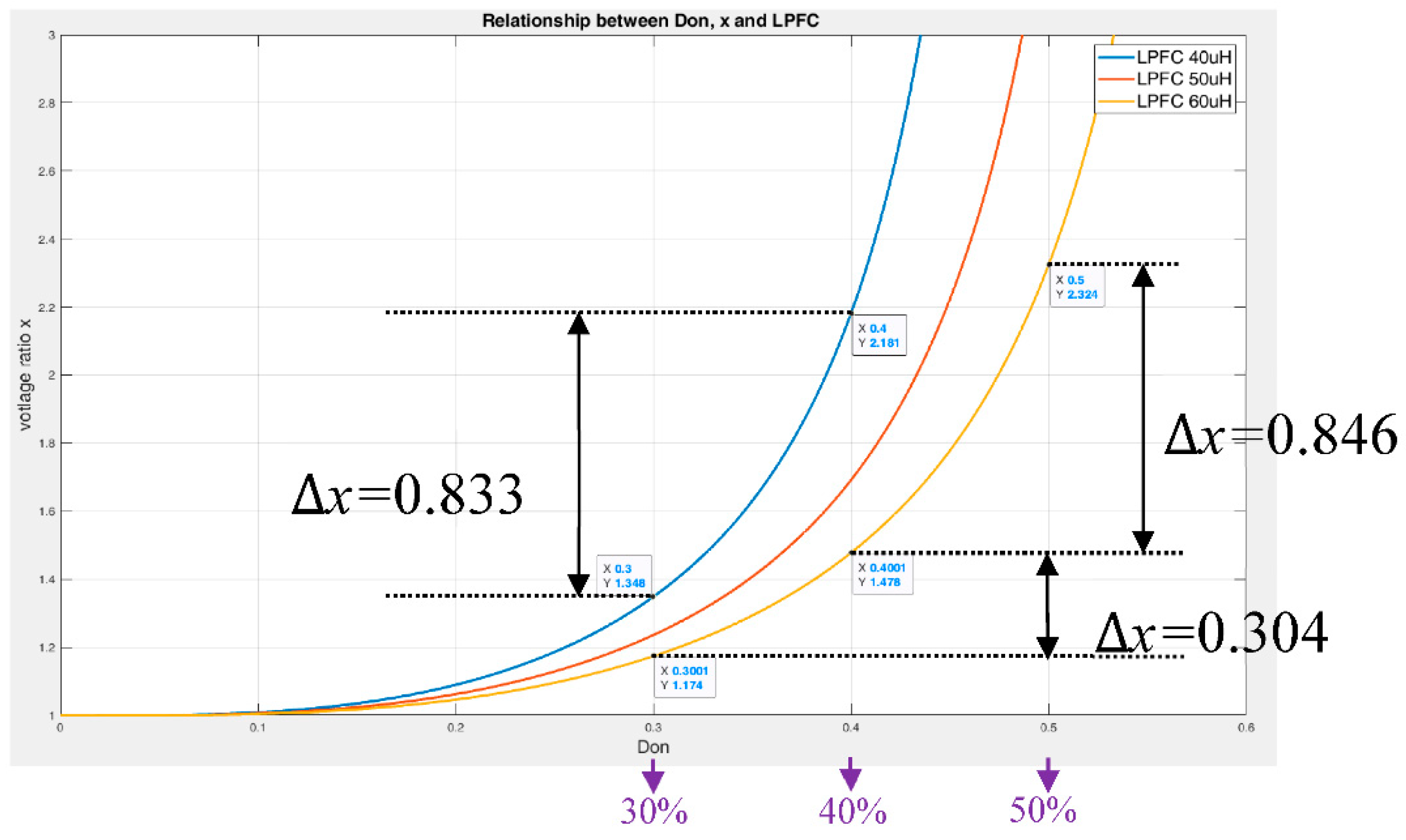
Equation (14) can be derived from Figure 10 and references [14,15]. Where Vm represents the input peak voltage, Don is the duty cycle of S2, TS is the switching period, and x is the voltage ratio, as shown in Equation (15). After combining Equations (14) and (15), Figure 11 can be obtained. The x-axis represents Don, and y-axis represents voltage ratio x. Through a single curve, it can be noticed that the range of x will increase during the increment of Don. In order to avoid excessive variation of the output voltage, Don is set under 40%. Different curves can be compared under the same variation range of Don. Take the range of Don varying from 30% to 40% as an example, x increases to 0.304 with LPFC of 60 μH, but x increases to 0.833 with LPFC of 40 μH. It can be seen that the smaller inductance causes a higher voltage variation range. Larger variation of x also causes a higher voltage spike to increase the switching loss during the transient time. To avoid the higher voltage variation, the inductance of LPFC should be higher. However, if LPFC is high, iLPFC still has to be in discontinuous conduction mode at the same time to avoid the decrement of power factor. If the converter operates in heavy load condition or the peak value of iLPFC goes to continuous conduction mode, these impacts will decrease the power factor. Therefore, the trade-off between loss and the power factor for the inductance of LPFC should be designed carefully.
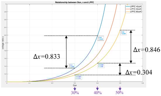
Figure 11.
Relationship between Don and x.
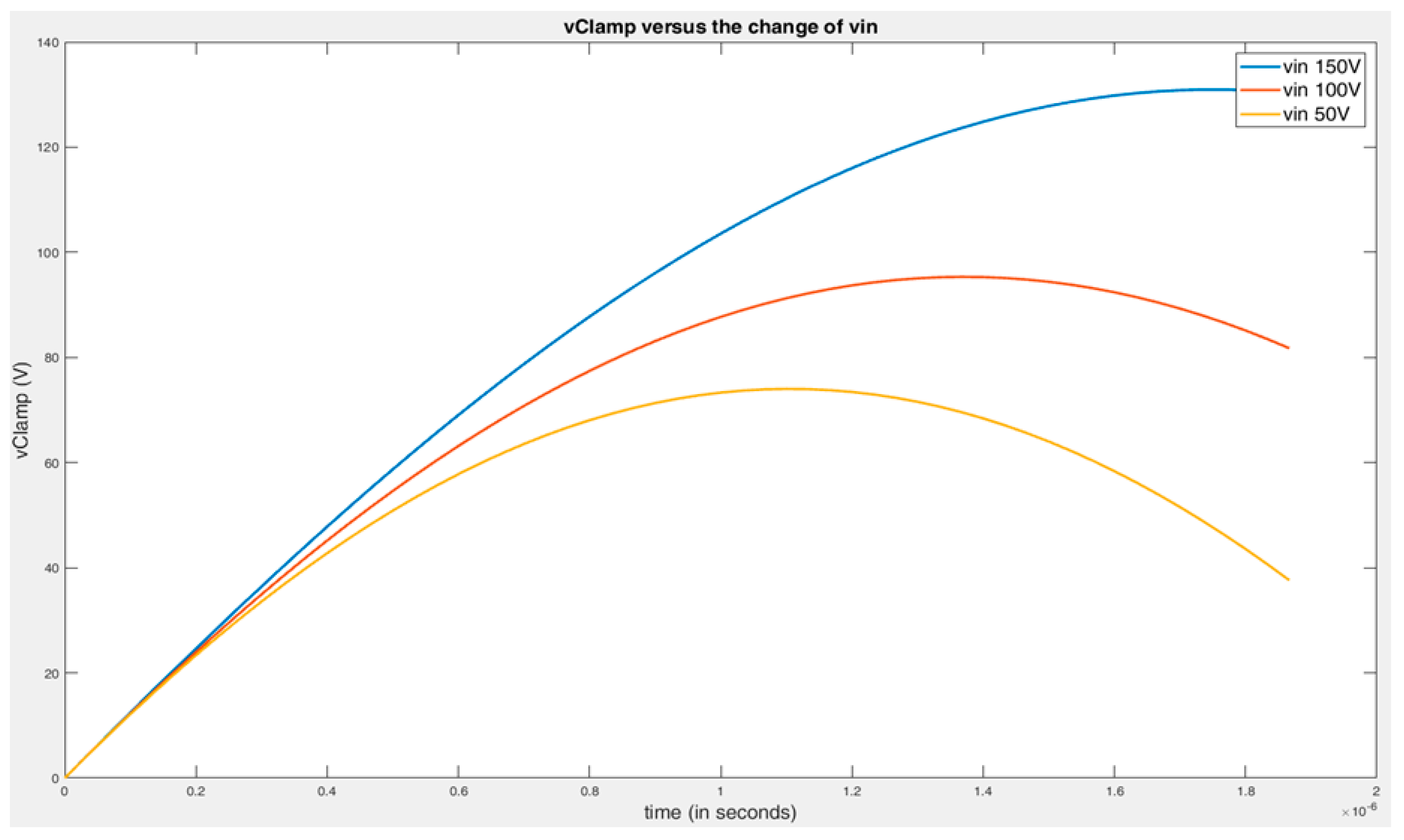
To compare with the conventional boost topology for single stage structure [16], the power factor correction stage includes CClamp in the proposed topology. Figure 12 can be obtained through Equation (2) under different vin. Noticing vClamp is influenced by vin, the value of vDS1 and vDS2 will be influenced as well. Therefore, the value of CClamp is related to the switching loss of the primary switches. In Figure 12, the x-axis represents the time and the y-axis represents vClamp.
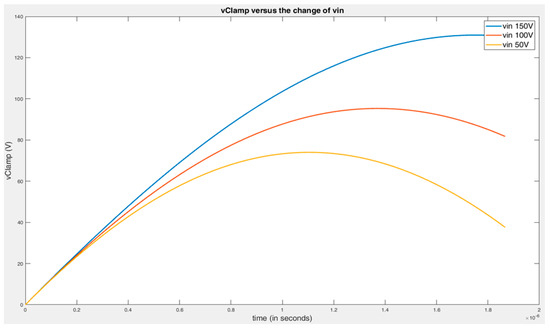
Figure 12.
Relationship between vClamp and vin.
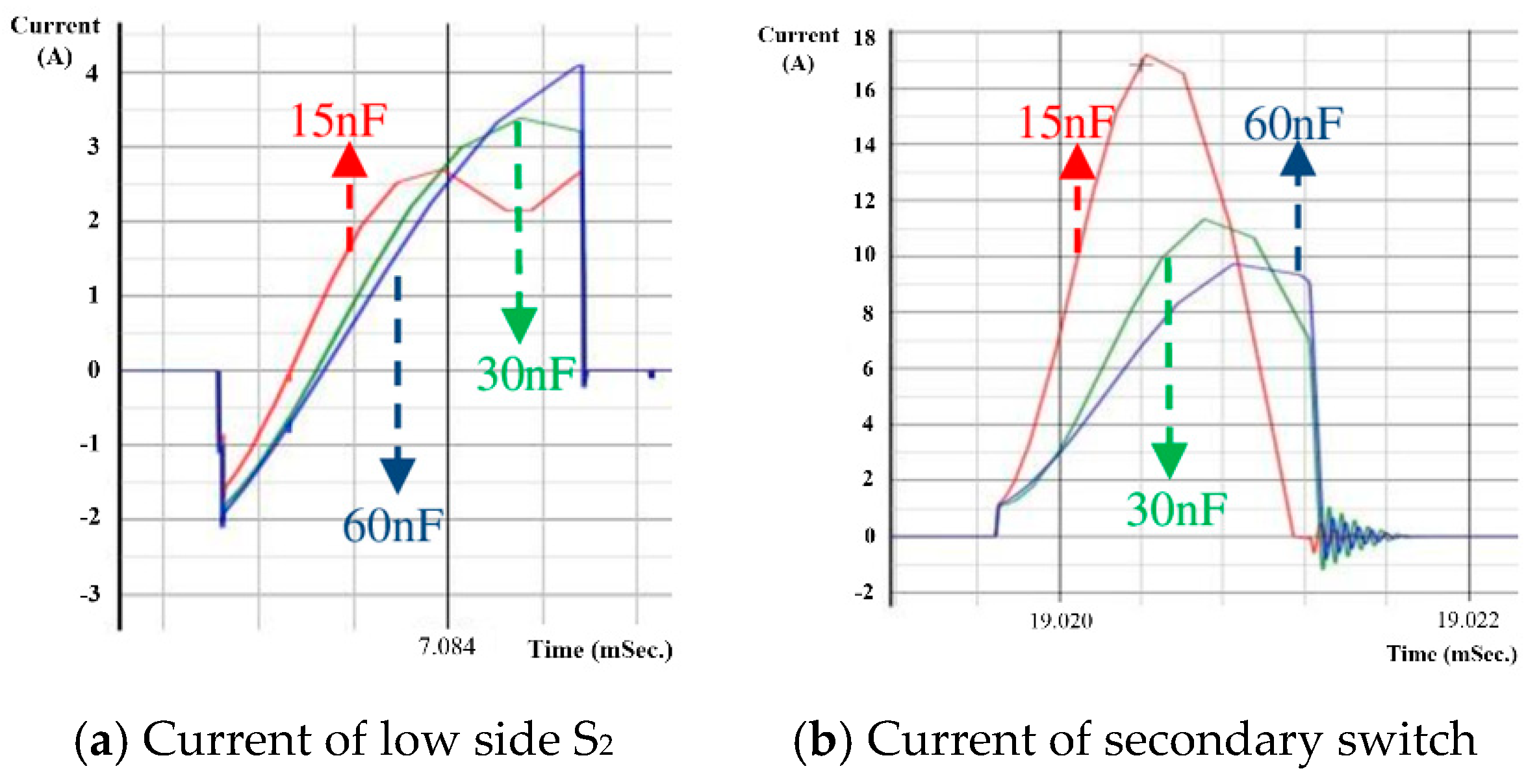
CClamp and Lr are the main resonant components when S2 turns on. The resonant period Tr between the two elements is about twice of the turn-on time when S2 is on as shown in Equation (16). CClamp will affect the switching loss and the capacitance of CClamp can be further optimized by SIMetrix software. As shown in Figure 13a, the smaller capacitance can reduce the switching loss of S2. In the meanwhile, from Figure 13b, this will also increase the conduction loss of the synchronous rectifier switch at the secondary side. That is, the smaller capacitance causes higher current at the secondary side. Therefore, the capacitance selection of CClamp should be considered carefully.
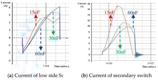
Figure 13.
(a,b) The current influence from CClamp.
Since S2 needs to withstand the current stress from LPFC and CClamp in mode 4 and 5, the switching loss of S2 has a great impact for the efficiency. In order to reduce the switching loss caused by S2, the value of Lm is designed to be larger than Lm(min) to reduce the peak current at the primary side. By using the voltage-second balancing law, Equation (17) can be obtained. Where Lm(min) represents the minimum inductance of the continuous conduction mode. In this proposed topology, Lm(min) is twice that of the conventional single transformer connection under this condition. This design consideration makes S1 have no ZVS function without Lm, which causes the failure of ZVS at the valley part. However, the overall efficiency still can be improved by reducing the switching loss of S2.
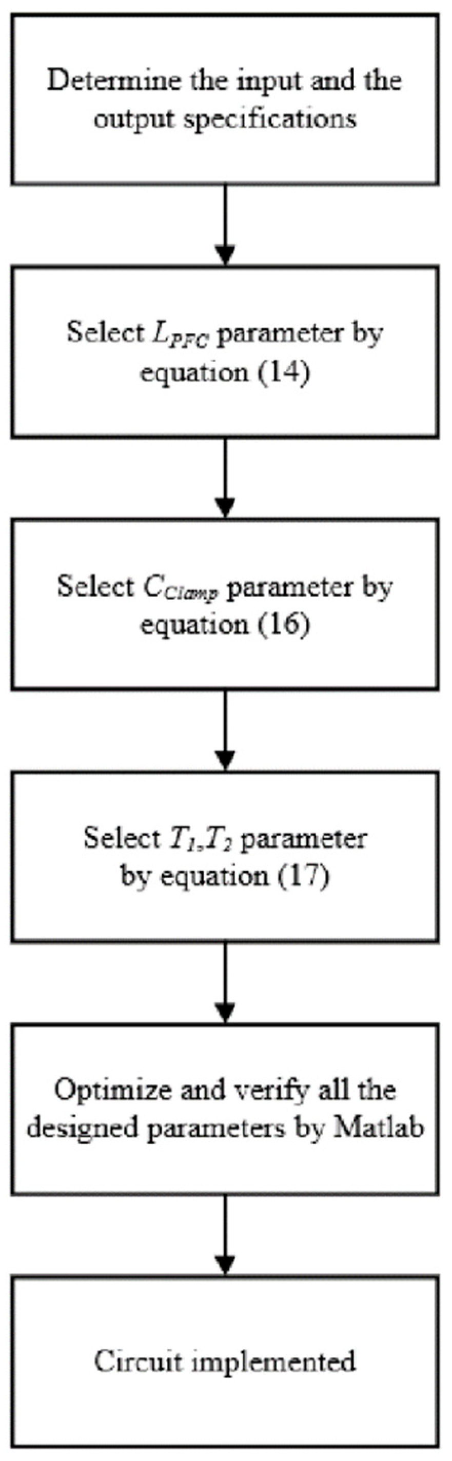
A step-by-step design flow chart of proposed converter is shown in Figure 14. The parameters of the converter can be acquired step by step. At first, the input and the output specifications have to be determined. Then, the following parameters of key components can be calculated by using Equations (14), (16) and (17). After all the key components are obtained, the optimization with Matlab is verified to avoid LPFC entering into CCM or ZVS failure. Finally, the circuit can be implemented efficiently.
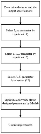
Figure 14.
Design flow chart of proposed converter.
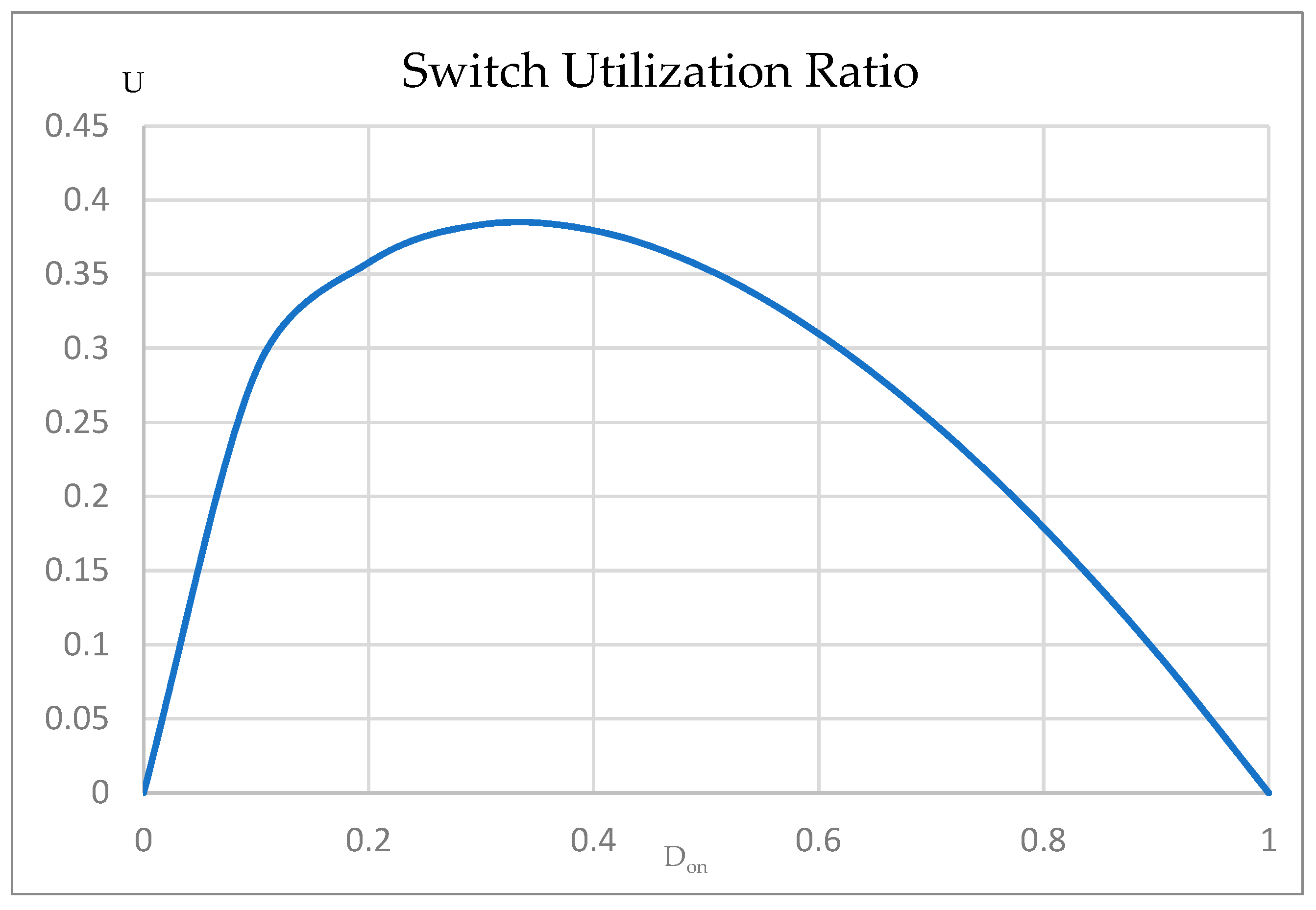
2.4. Switch Utilization Ratio
The definition of switch utilization ratio (U) is the output power of the converter circuit derived per unit of switch stress. For this study, the proposed ACF converter of Don is set for 0.35 in practical design consideration. Therefore, the peak of U is 0.385 from the figure. The curve of U is plotted as shown in Figure 15.

Figure 15.
Switch utilization ratio with different Don.
2.5. Steady-State Voltage Gain with Varying Duty
In Figure 16, the steady-state voltage gain is depicted with varying duty-cycle. It shows a curve of the steady-state voltage gain response of the proposed converter for the duty-cycle changing from 10% to 100%.
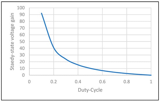
Figure 16.
Steady-state voltage gain with different duty.
3. Experimental and Simulation Result
The specification of the proposed circuit is shown in Table 2, and Table 3 shows the parameters of the proposed circuit. Lr is the total leakage inductance of the dual transformers.
Table 2.
Circuit specification.
Table 3.
Component parameters.
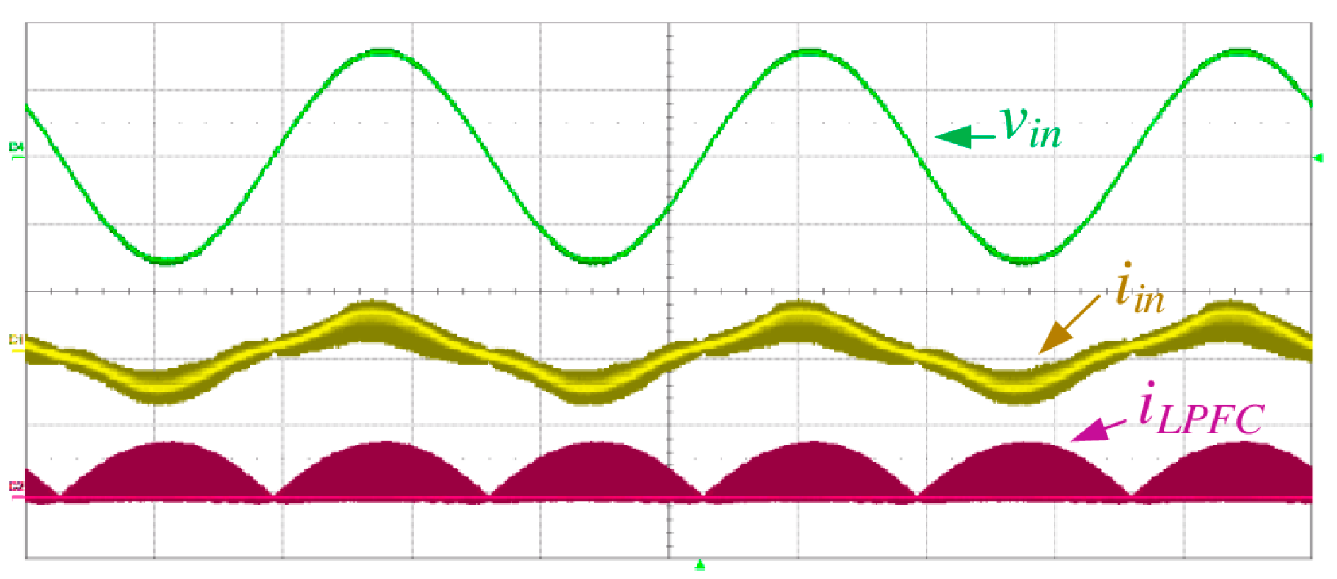
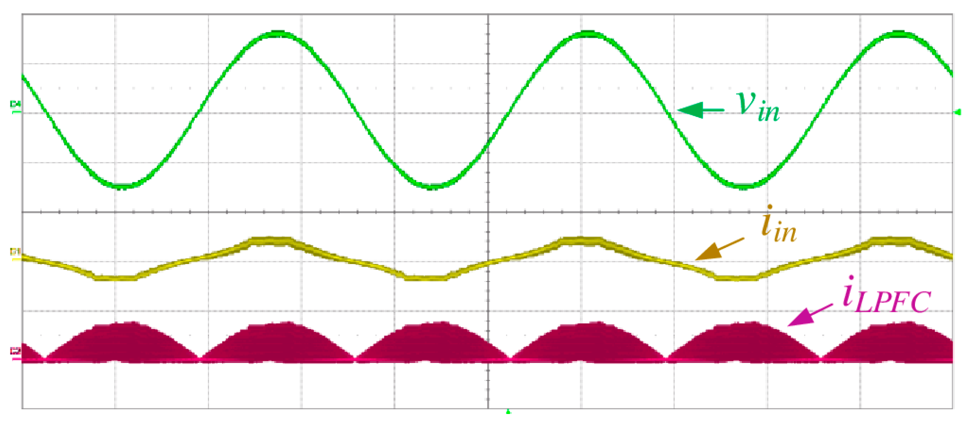
Figure 17 shows the waveforms of input voltage vin, current iin, and iLPC under light load 30 W. Figure 18 shows the waveform of full load 120 W. Since iLPFC is designed for discontinuous conduction mode, the power factor correction function can be achieved without detecting input signals.

Figure 17.
Input and iLPFC waveforms under light load condition vin: 100 V/div, iLPFC: 2 A/div, iin: 1 A/div, Time: 5 ms/div.
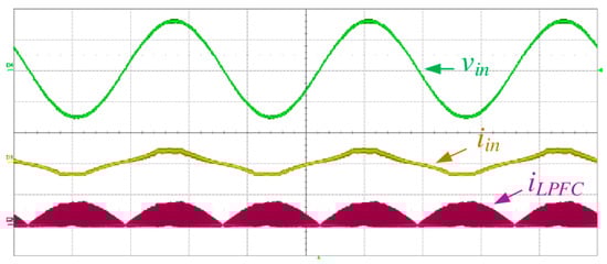
Figure 18.
Input and iLPFC waveforms under full load condition vin: 100 V/div, iLPFC: 5 A/div, iin: 5 A/div, Time: 5 ms/div.
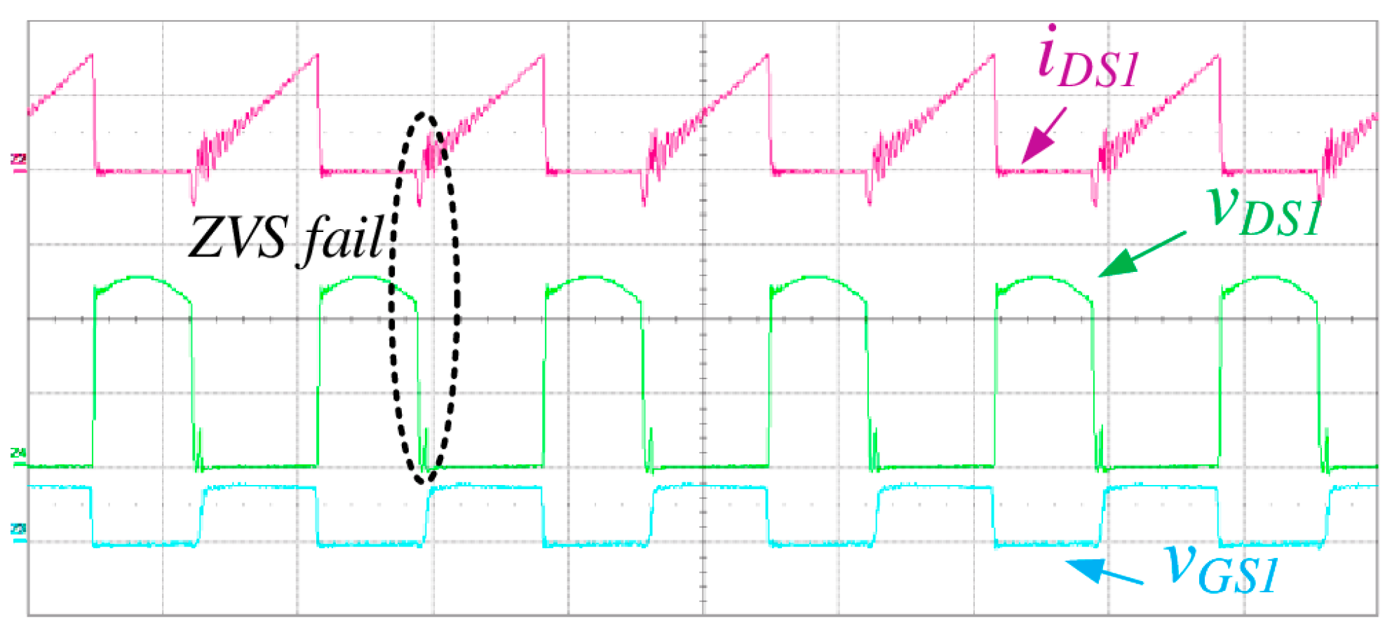
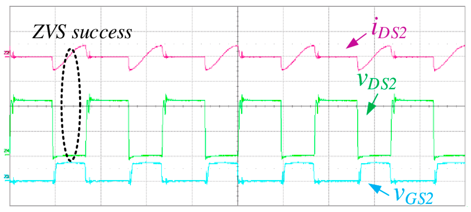
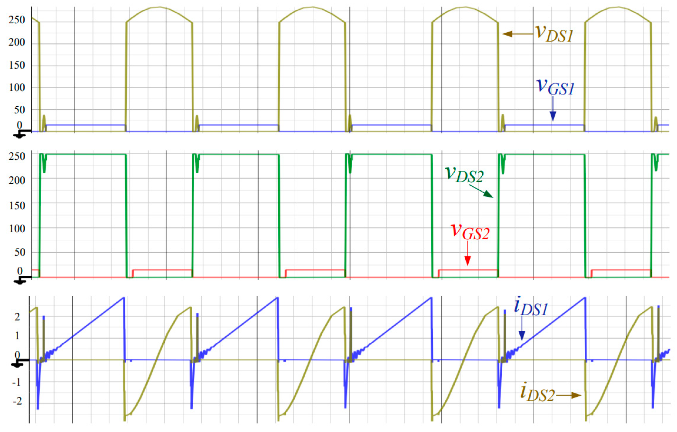
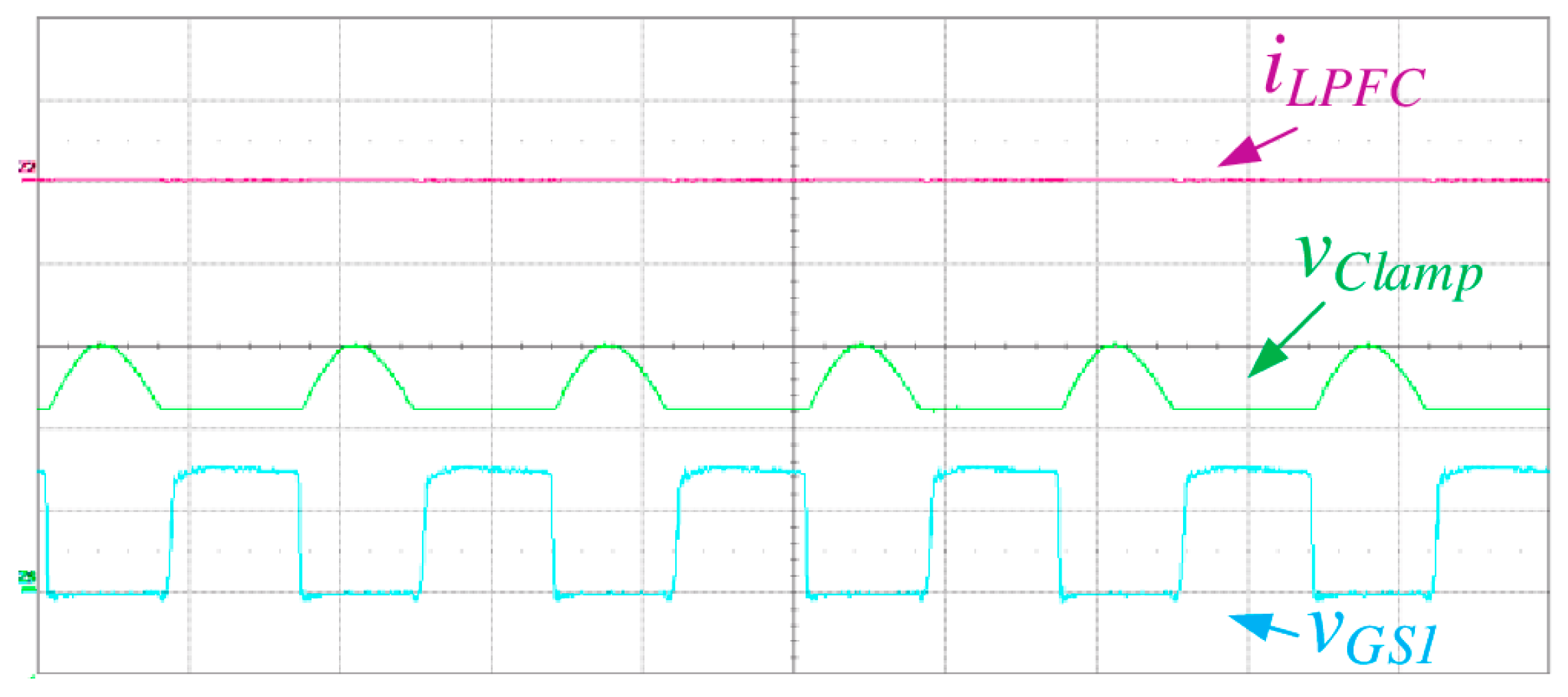
The waveforms are measured at valley, middle, and peak points individually under full load condition. In order to reduce the switching loss on S2, Lm is designed to be larger than Lm(min) for lowering the peak current. This situation causes iLm to be positive during valley point. ZVS of S1 will fail without Lm in mode 6 shown Figure 19. On the other hand, S2 will achieve ZVS through the current of Lr, Lm1, and Lm2 shown in Figure 20. Figure 21 shows the simulation waveforms during the valley point to verify the experimental results. As shown in Figure 22, Lr and CClamp only resonate during the turn off time of S1, which is much shorter than the middle point and the valley point during the resonant time.
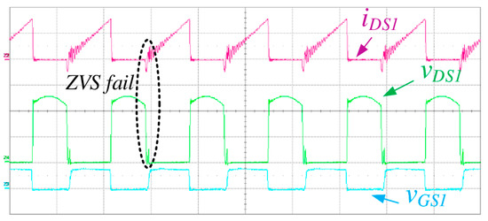
Figure 19.
S1’s waveform during valley point iDS1: 2 A/div, vDS1: 100 V/div, vGS1:20 V/div, Time: 2 μs/div.
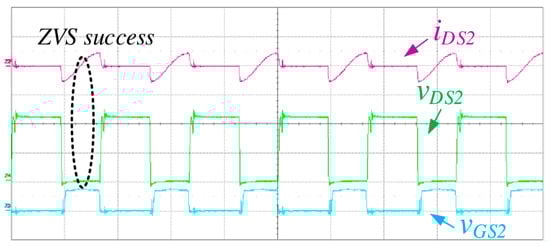
Figure 20.
S2’s waveform during valley point iDS2: 5 A/div, vDS2: 100 V/div, vGS2:20 V/div, Time: 2 μs/div.
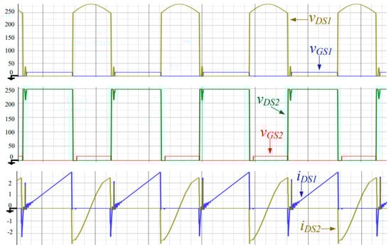
Figure 21.
Simulation of S1 and S2 related waveform during valley point, Time: 2 μs/div.
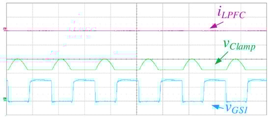
Figure 22.
CClamp related waveforms during valley point iLPFC: 5 A/div, vClamp: 50 V/div, vGS1:10 V/div, Time: 2 μs/div.
At the middle point under the full load condition, iLPFC helps the negative current to flow through S1 for achieving ZVS in mode 1 as shown in Figure 23. From Figure 24, they show the period resonated by LPFC and CClamp. In this situation, the extension of resonant time for vClamp will also influence S1 and S2’s switching loss. S2 achieves ZVS through the current from Lr, Lm1, and Lm2 in mode 2 as shown in Figure 25. In Figure 26, it shows the simulation waveforms to verify the experimental results. Because the current of S2 is the summation of iLr and iLPFC, the peak of iDS2 will increase when iLPFC increases.
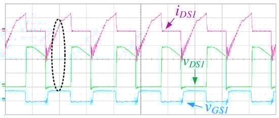
Figure 23.
S1’s waveform during middle point iDS1: 2 A/div, vDS1: 100 V/div, vGS1:20 V/div, Time: 2 μs/div.
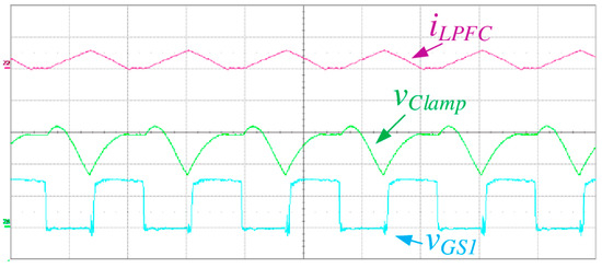
Figure 24.
CClamp relation waveforms during middle point iLPFC: 5 A/div, vClamp: 50 V/div, vGS1:10 V/div, Time: 2 μs/div.
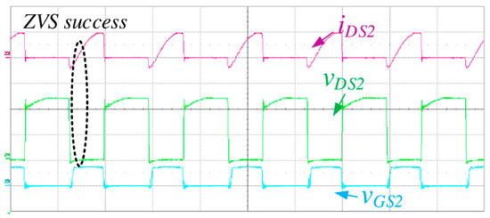
Figure 25.
S2’s waveform during middle point iDS2: 5 A/div, vDS2: 100 V/div, vGS2:20 V/div, Time: 2 μs/div.
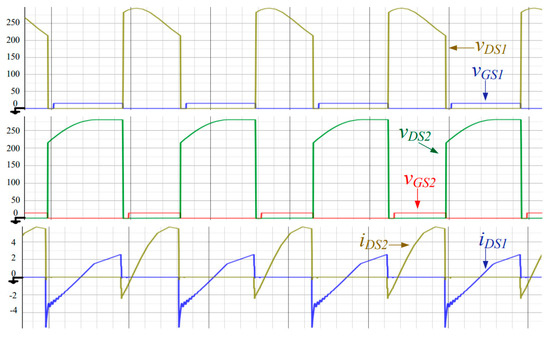
Figure 26.
Simulation of S1 and S2 related waveform during middle point, Time: 2 μs/div.
Due to the negative current of iLPFC, S1 can easily achieve ZVS function at the peak point as shown in Figure 27. S2 also achieves ZVS by the total current of Lr, Lm1, and Lm2 as shown in Figure 28. Under the influence of vClamp’s variation, the higher vDS1 with the lower iDS1 occurs at the moment when S1 turns off momentarily. On the other hand, the higher iDS2 with the lower vDS2 occurs at the moment when S2 turns off instantaneously. This complementary situation is achieved by the appropriate selection of the clamping capacitance. As shown in Figure 29, it can be seen that the charging and discharging behavior of vClamp is most severe at the peak point, which reduces the switching loss caused by S2 indirectly. In Figure 30, the simulation waveform during the peak point is shown to verify the experimental results.
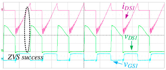
Figure 27.
S1’s waveform during peak point iDS1: 2 A/div, vDS1: 100 V/div, vGS1:20 V/div, Time: 2 μs/div.
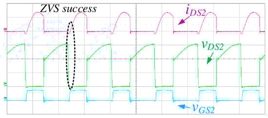
Figure 28.
S2’s waveform during peak point iDS2: 2 A/div, vDS2: 100 V/div, vGS2:20 V/div, Time: 2 μs/div.
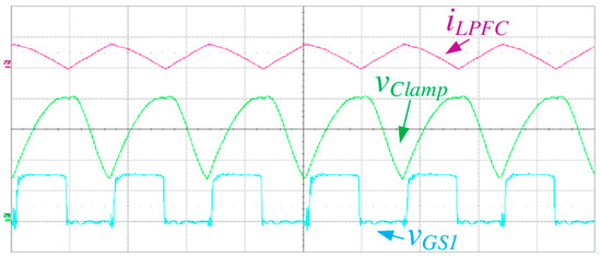
Figure 29.
CClamp related waveforms during peak point iLPFC: 5 A/div, vClamp: 50 V/div, vGS1:10 V/div, Time: 2 μs/div.
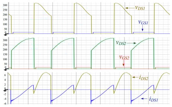
Figure 30.
Simulation of S1 and S2 related waveform during peak point, Time: 2 μs/div.
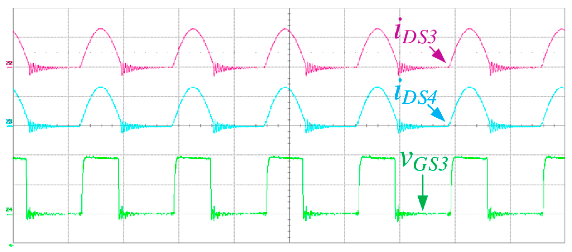
Because of the extension of Lr and CClamp’s resonant time, the waveform of iDS2 will be affected. The difference of iDS2 between Figure 20 and Figure 28 can clearly be seen. This situation will further affect the waveforms of iDS3 and iDS4. From Figure 31, the current of iDS3 and iDS4 are smaller at the secondary side for reducing the switching loss of S3 and S4 effectively.
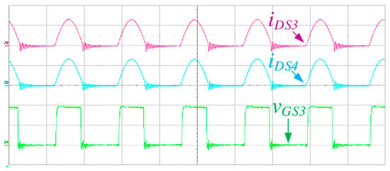
Figure 31.
CClamp related waveforms during peak point iDS3: 10 A/div, iDS4: 10 A/div, vGS3:5 V/div, Time: 2 μs/div.
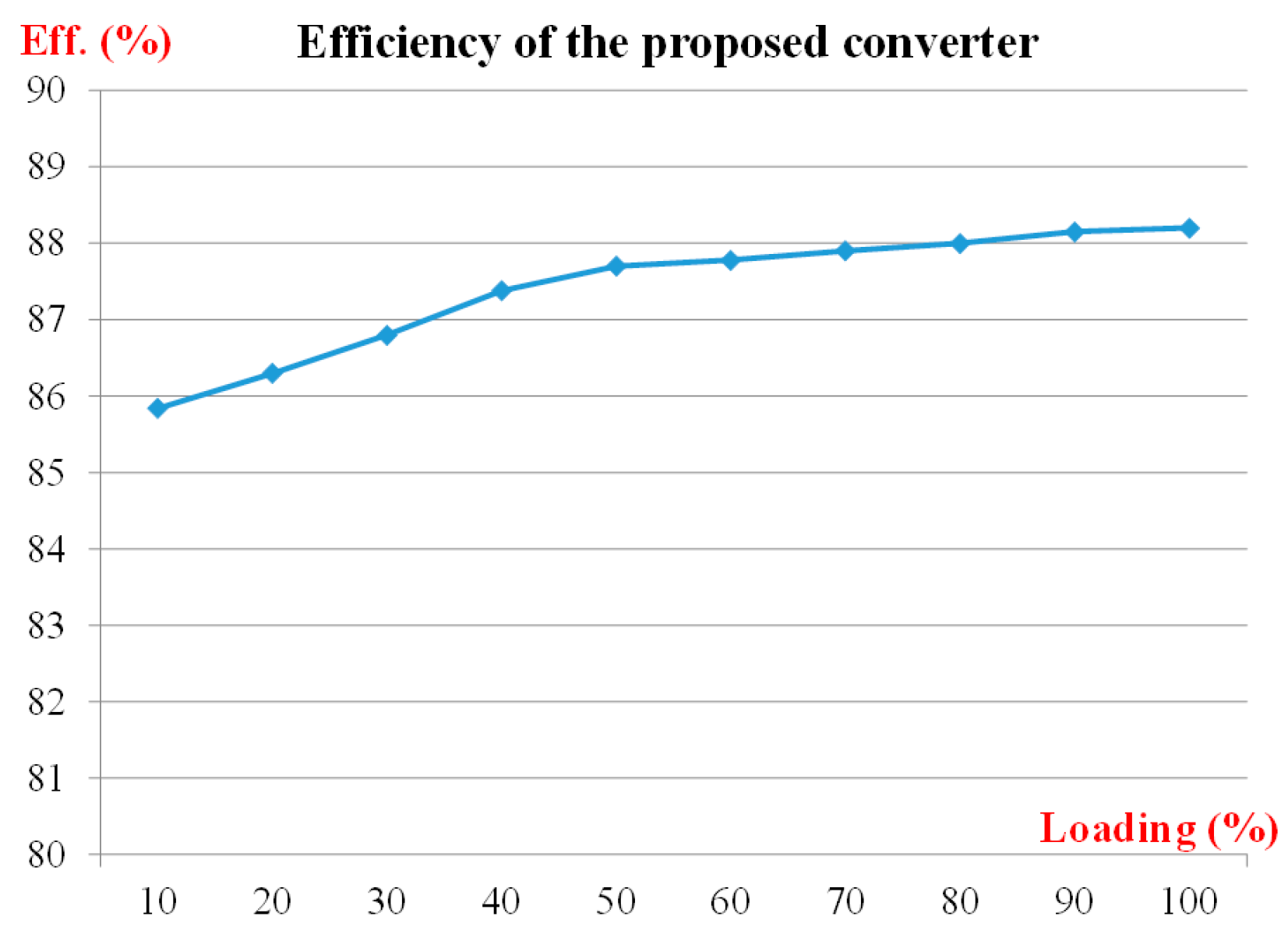
In Figure 32, the efficiency of the proposed converter is measured and summarized. At light load condition, the efficiency starts from 85.8%. When the output goes to full load, the efficiency reaches 88.20%.
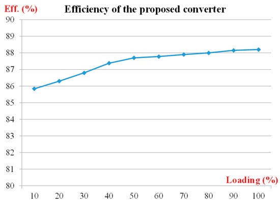
Figure 32.
Efficiency of proposed converter with different loading.
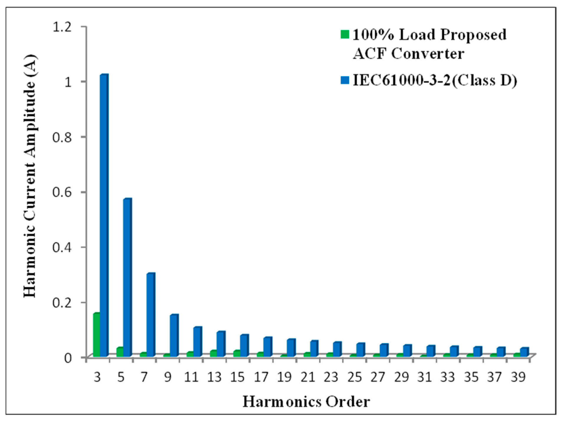
In addition, harmonic current is also a key factor to verify the PFC function. In Figure 29, the harmonic current of the proposed converter is measured which is shown in green bars. Moreover, the standard of IEC-61000-3-2 is compared which is shown in blue bars. Based on Figure 33, the current of odd-harmonic is lower than the standard.

Figure 33.
Comparison of harmonic current between IEC-61000-3-2 and the proposed scheme.
Due to the single-stage structure, the two switches at the primary side should withstand the current stress from both side of PFC and ACF stage as shown in mode 1 and mode 5. This will cause switching loss and conduction loss on these two switches to dominate a major part of the total loss for this circuit, especially for higher switching frequency. To compare with CCM PFC converters for detecting AC input signal, the proposed topology has a slightly higher THD causing PF to drop slightly. The reason is that the designed LPFC needs to keep the PFC current operating in DCM for low power applications, and there is no need to detect any input signal.
As shown in Table 4, after the measurements, the power factor and the efficiency reached 0.977 and 85.84% under light load. At full load condition, the power factor reached 0.984 and the efficiency goes to 88.20%. Table 5 also shows a calculation for power loss of these switches under full load condition.
Table 4.
Experimental measurement.
Table 5.
Power losses calculation on the switches at primary and secondary sides [30].
The prototype of the proposed single-stage PFC active-clamp flyback converter with dual transformers is shown in Figure 34. The output power is 120 W (19 V, 6.32 A) which is suitable for laptop adaptor application. The dimension is measured in centimeters (12.5 cm × 15 cm).
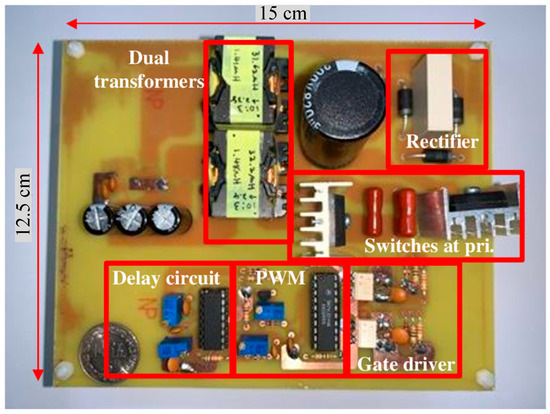
Figure 34.
Prototype of the proposed single-stage PFC ACF with dual transformers.
4. Conclusions
This paper proposes a single-stage active clamp flyback converter with dual transformers in series and parallel connection which is implemented. Through the proposed design, the PFC inductor assists the negative current path of the high-side power switch S1 for achieving ZVS without any additional inductors except the rectified voltage drops to the valley point. The proposed design can not only decrease the switching loss but also lower the number of the components. S2 can also achieve ZVS by the magnetizing current from the dual transformers.
By connecting the dual transformers in series connection at primary side and parallel connection at secondary side, the copper loss and the conduction loss can be saved effectively. The efficiency of 88.20% with power factor 0.984 under full load condition has been achieved.
Author Contributions
S.-T.W. conceptualized and supervised the experiments of the research. S.-T.W. revised and modified the research data into paper format. Y.-T.C. Cheng was in charge of environment building up. Y.-T.C. Cheng was in charge of measurement and data recording. All authors have read and agreed to the published version of the manuscript.
Funding
This research is supported by Ministry of Science and Technology. The project number of the foundation: MOST 110-2221-E-150-017.
Institutional Review Board Statement
Not applicable.
Informed Consent Statement
Not applicable.
Data Availability Statement
Data sharing not applicable.
Conflicts of Interest
The authors declare no conflict of interest.
References
- Dawson, G.; Chan, I.N. A Modified Zero-Voltage-Switching Flyback Converter. IEEE Trans. Power Electron. 1994, 9, 129–135. [Google Scholar]
- Zhang, J.; Huang, X.; Wu, X.; Qian, Z. A High Efficiency Flyback Converter with New Active Clamp Technique. IEEE Trans. Power Electron. 2010, 25, 1775–1785. [Google Scholar] [CrossRef]
- Lee, H.; Choe, H.; Ham, S.; Kang, B. High-Efficiency Asymmetric Forward-Flyback Converter for Wide Output Power Range. IEEE Trans. Power Electron. 2017, 32, 433–440. [Google Scholar] [CrossRef]
- Hakoda, Y.; Ninomiya, T.; Shoyama, M.; Hashimoto, T. Effect of Clamp Capacitor on the Stability of Active-Clamp DC-DC Converters. In Proceedings of the PESC 98 Record. 29th Annual IEEE Power Electronics Specialists Conference (Cat. No.98CH36196), Fukuoka, Japan, 22 May 1998; pp. 355–361. [Google Scholar]
- Chiu, H.J.; Lo, Y.K.; Lee, H.C.; Cheng, S.J.; Yan, Y.C.; Lin, C.Y.; Wang, T.H.; Mou, S.C. A Single-Stage Soft-Switching Flyback Converter for Power-Factor Correction Applications. IEEE Trans. Ind. Electron. 2010, 57, 2187–2190. [Google Scholar] [CrossRef]
- Xue, L.; Zhang, J. Highly Efficient Secondary-Resonant Active Clamp Flyback Converter. IEEE Trans. Ind. Electron. 2018, 65, 1235–1243. [Google Scholar] [CrossRef]
- Perrin, R.; Quentin, N.; Allard, B.; Martin, C.; Ali, M. High Temperature GaN Active-Clamp Flyback Converter with Resonant Operation Mode. IEEE J. Emerg. Sel. Top. Power Electron. 2016, 4, 1077–1085. [Google Scholar] [CrossRef]
- Spiazzi, G.; Mattavelli, P.; Costabeber, A. High Step-Up Ratio Flyback Converter with Active Clamp and Voltage Multiplier. IEEE Trans. Power Electron. 2011, 26, 3205–3214. [Google Scholar] [CrossRef]
- Papanikolaou, N.P.; Tatakis, E.C. Active Voltage Clamp in Flyback Converters Operating in CCM Mode Under Wide Load Variation. IEEE Trans. Ind. Electron. 2004, 51, 632–640. [Google Scholar] [CrossRef]
- Wu, T.F.; Lai, Y.S.; Hung, J.C.; Chen, Y.M. Boost Converter with Coupled Inductors and Buck-Boost Type of Active Clamp. IEEE Trans. Ind. Electron. 2008, 55, 154–162. [Google Scholar] [CrossRef]
- Lin, B.R.; Dong, J.Y. Analysis and Implementation of an Active Clamping Zero-Voltage Turn-On Switching/Zero-Current Turn-Off Switching Converter. IET Power Electron. 2010, 3, 429–437. [Google Scholar] [CrossRef]
- Kyu-Chan, L.; Hang-Seok, C.; Bo Hyung, C. Power Factor Correction Converter Using Delay Control. IEEE Trans. Power Electron. 2000, 15, 626–633. [Google Scholar] [CrossRef]
- Tse, C.K.; Chow, M.H.L. New Single-Stage Power-Factor-Corrected Regulators Operating in Discontinuous Capacitor Voltage Mode. In Proceedings of the PESC97. Record 28th Annual IEEE Power Electronics Specialists Conference. Formerly Power Conditioning Specialists Conference 1970–1971. Power Processing and Electronic Specialists Conference 1972, St. Louis, MO, USA, 27 June 1997; pp. 371–377. [Google Scholar]
- Duranay, Z.B.; Guldemir, H. Simulation of Power Factor Corrected AC-DC Boost Converter. In Proceedings of the 2019 11th International Conference on Electronics, Computers and Artificial Intelligence (ECAI), Pitesti, Romania, 27–29 June 2019; pp. 1–4. [Google Scholar]
- Korotkov, S.; Miffakhutdinov, R.; Nemchinov, A.; Fraidlin, S. Asymmetrical Half-Bridge in a Single Stage PFC AC/DC Converter. In Proceedings of the APEC 97—Applied Power Electronics Conference, Atlanta, GA, USA, 27 February 1997; pp. 484–488. [Google Scholar]
- Redl, R. An Economical Single-Phase Passive Power-Factor-Corrected Rectifier: Topology, Operation, Extensions, and Design for Compliance. In Proceedings of the APEC 98. Thirteenth Annual Applied Power Electronics Conference and Exposition, Anaheim, CA, USA, 15–19 February 1998; pp. 454–460. [Google Scholar]
- Park, J.; Roh, Y.S.; Moon, Y.J.; Yoo, C. A CCM/DCM Dual-Mode Synchronous Rectification Controller for a High-Efficiency Flyback Converter. IEEE Trans. Power Electron. 2014, 29, 768–774. [Google Scholar] [CrossRef]
- Kwon, J.M.; Kwon, B.H. High Step-Up Active-Clamp Converter with Input-Current Doubler and Output-Voltage Doubler for Fuel Cell Power Systems. IEEE Trans. on Power Electron. 2009, 24, 108–115. [Google Scholar] [CrossRef]
- Lin, B.R.; Chiang, H.K.; Chen, C.C. Analysis of a Zero-Voltage Switching Converter with Two Transformers. IEEE Trans. Circuits Syst. II 2006, 53, 1088–1092. [Google Scholar] [CrossRef]
- Lee, J.J.; Kwon, J.M.; Kim, E.H.; Kwon, B.H. Dual Series-Resonant Active-Clamp Converter. IEEE Trans. Ind. Electron. 2008, 55, 699–710. [Google Scholar] [CrossRef]
- Li, W.; Zhao, Y.; Deng, Y.; He, X. Interleaved Converter with Voltage Multiplier Cell for High Step-Up and High-Efficiency Conversion. IEEE Trans. on Power Electron. 2010, 25, 2397–2408. [Google Scholar] [CrossRef]
- Lee, Y.S.; Lin, B.T. Adding Active Clamping and Soft Switching to Boost-Flyback Single-Stage Isolated Power-Factor-Corrected Power Supplies. IEEE Trans. Power Electron. 1997, 12, 1017–1027. [Google Scholar]
- Xu, H.; Chen, D.; Xue, F.; Li, X. Optimal Design Method of Interleaved Boost PFC for Improving Efficiency from Switching Frequency, Boost Inductor and Output Voltage. IEEE Trans. Power Electron. 2019, 34, 6088–6107. [Google Scholar] [CrossRef]
- Watson, R.; Lee, F.C.; Hua, G.C. Utilization of an Active-Clamp Circuit to Achieve Soft Switching in Flyback Converters. IEEE Trans. Power Electron. 1996, 11, 162–169. [Google Scholar] [CrossRef]
- Lin, W.; Chen, H.; Fang, Y. A Single-stage PFC by integrating quasi-bridgeless boost and LLC converter. In Proceedings of the 2018 IEEE International Telecommunications Energy Conference (INTELEC), Turino, Italy, 7–11 October 2018. [Google Scholar]
- Usman, R.; Ali Faisal, M.; Hadeed, A.S.; Dario, G. Design and Analysis of a Novel High-Gain DC-DC Boost Converter with Low Component Count. Electronics 2021, 10, 1761. [Google Scholar]
- Abasian, A.; Farzanehfard, H.; Hashem, S.A. A Single-Stage Single-Switch Soft-Switching (S6) Boost-Flyback PFC Converter. IEEE Trans. Power Electron. 2019, 34, 9806–9813. [Google Scholar] [CrossRef]
- Liu, Y.M.; Chang, L.K. Single-Stage Soft-Switching AC–DC Converter with Input-Current Shaping for Universal Line Applications. IEEE Trans. Ind. Electron. 2009, 56, 467–479. [Google Scholar]
- Lee, S.W.; Do, H.L. Soft-Switching Two-Switch Resonant AC–DC Converter with High Power Factor. IEEE Trans. Ind. Electron. 2016, 63, 2083–2091. [Google Scholar] [CrossRef]
- Shen, Y.; Zhao, W.; Chen, Z.; Cai, C. Full-Bridge LLC Resonant Converter With Series-Parallel Connected Transformers for Electric Vehicle On-Board Charger. IEEE Access 2018, 6, 13490–13500. [Google Scholar] [CrossRef]


Publisher’s Note: MDPI stays neutral with regard to jurisdictional claims in published maps and institutional affiliations. |
© 2021 by the authors. Licensee MDPI, Basel, Switzerland. This article is an open access article distributed under the terms and conditions of the Creative Commons Attribution (CC BY) license (https://creativecommons.org/licenses/by/4.0/).