Article

Hardware Implementation Study of Particle Tracking Algorithm on FPGAs

by
Alessandro Gabrielli
1,2,*,
Fabrizio Alfonsi
2,
Alberto Annovi
3,
Alessandra Camplani
4 and
Alessandro Cerri
5
1
Department of Physics and Astronomy, University of Bologna, 40126 Bologna, Italy
2
INFN Bologna, Viale Berti Pichat 6/2, 40127 Bologna, Italy
3
INFN Pisa, 56127 Pisa, Italy
4
Niels Bohr Institute, Copenhagen University, 1165 København, Denmark
5
School of Mathematical and Physical Sciences, University of Sussex, Brighton BN1 9RH, UK
*
Author to whom correspondence should be addressed.
Electronics 2021, 10(20), 2546; https://doi.org/10.3390/electronics10202546
Submission received: 30 August 2021 / Revised: 22 September 2021 / Accepted: 12 October 2021 / Published: 18 October 2021
(This article belongs to the Special Issue VLSI Circuits & Systems Design)

Abstract

:
In recent years, the technological node used to implement FPGA devices has led to very high performance in terms of computational capacity and in some applications these can be much more efficient than CPUs or other programmable devices. The clock managers and the enormous versatility of communication technology through digital transceivers place FPGAs in a prime position for many applications. For example, from real-time medical image analysis to high energy physics particle trajectory recognition, where computation time can be crucial, the benefits of using frontier FPGA capabilities are even more relevant. This paper shows an example of FPGA hardware implementation, via a firmware design, of a complex analytical algorithm: The Hough transform. This is a mathematical spatial transformation used here to facilitate on-the-fly recognition of the trajectories of ionising particles as they pass through the so-called tracker apparatus within high-energy physics detectors. This is a general study to demonstrate that this technique is not only implementable via software-based systems, but can also be exploited using consumer hardware devices. In this context the latter are known as hardware accelerators. In this article in particular, the Xilinx UltraScale+ FPGA is investigated as it belongs to one of the frontier family devices on the market. These FPGAs make it possible to reach high-speed clock frequencies at the expense of acceptable energy consumption thanks to the 14 nm technological node used by the vendor. These devices feature a huge number of gates, high-bandwidth memories, transceivers and other high-performance electronics in a single chip, enabling the design of large, complex and scalable architectures. In particular the Xilinx Alveo U250 has been investigated. A target frequency of 250 MHz and a total latency of 30 clock periods have been achieved using only the 17 ÷ 53% of LUTs, the 8 ÷ 12% of DSPs, the 1 ÷ 3% of Block Rams and a Flip Flop occupancy range of 9 ÷ 28%.

1. Introduction

High Energy Physics (HEP) aims to understand the structure of elementary particles, which are the fundamental constituents of matter. The great success of the so-called Standard Model (SM) has not only given us the interpretation of many interactions between particles, but also has built a basis for continuing to understand their nature. Beyond the SM we can begin to deeply explore the origin of matter in the Universe, what dark matter and dark energy are, the physics of the Big Bang and other untangled structures of space–time. To do this, the main experiments at the Large Hadron Collider (LHC) at CERN in Geneva (Switzerland) are now being updated to what is called Phase II high-luminosity upgrade [1]. In particular, the LHC experiments use detectors to study the particles produced by collisions in the accelerator. These experiments are carried out by huge collaborations of scientists from all over the world. Each experiment is unique and characterized by its detectors and the way in which the generated data are analyzed. In general, the data obtained through the detectors were filtered and grouped into physical Events [2]. Then, a complex off-line reconstruction put together the Events belonging to a common time slot, to make sure that they were generated almost simultaneously, being products of a common interaction. The Trigger [3] is an electronic system dedicated to the selection of potential physical data, among the huge amount of noise. More specifically, this Trigger is also a complex system made up of many internal components. The first of these, the one that makes the first selection, can be made of an electronic pattern recognition apparatus. It can also be composed of a relatively simple and fast analog device or it can be constituted by a more complex programmable digital system built with commercial components such as CPUs, GPUs and/or FPGAs. The study presented in this paper describes a recognition system based on the Hough Transform (HT) [4,5], implemented on a frontier FPGA. The proposed recognition system reads out that data originated in a detection system located close to the beam lines: The Tracker [6,7]. In addition, for HEP experiments that take years for the construction of the entire apparatus, it is not possible to test the hardware in a real environment in advance with respect to the final commissioning. These experiments are unique systems that cannot be fully reproduced elsewhere. However, parts of the system can be evaluated in advance using demonstrators that are used as proofs of concepts. With this study we have demonstrated, through post-layout simulations and performance comparisons, that the entire system can be implemented on a single FPGA. This is a proof of concept obtained in advance without incurring the high costs of this frontier electronics.

2. Hough Transform as Pattern Recognition Algorithm

The HT in general is a known extraction technique mainly implemented in image analysis and digital image processing. Over recent years other studies have proposed hardware implementations of the HT [8,9], but using smaller FPGAs and less aggressive target performance. The thousands of lanes processed in parallel in this design is something never investigated and this is to fulfill the specifications of the HEP experiments at CERN, which are unique in the field of physics research. Here, the HT algorithm is used as a tracking method for pattern recognition. In more details, it is used to extract trajectories, straight or curved lines within digital images representing the particle space. 
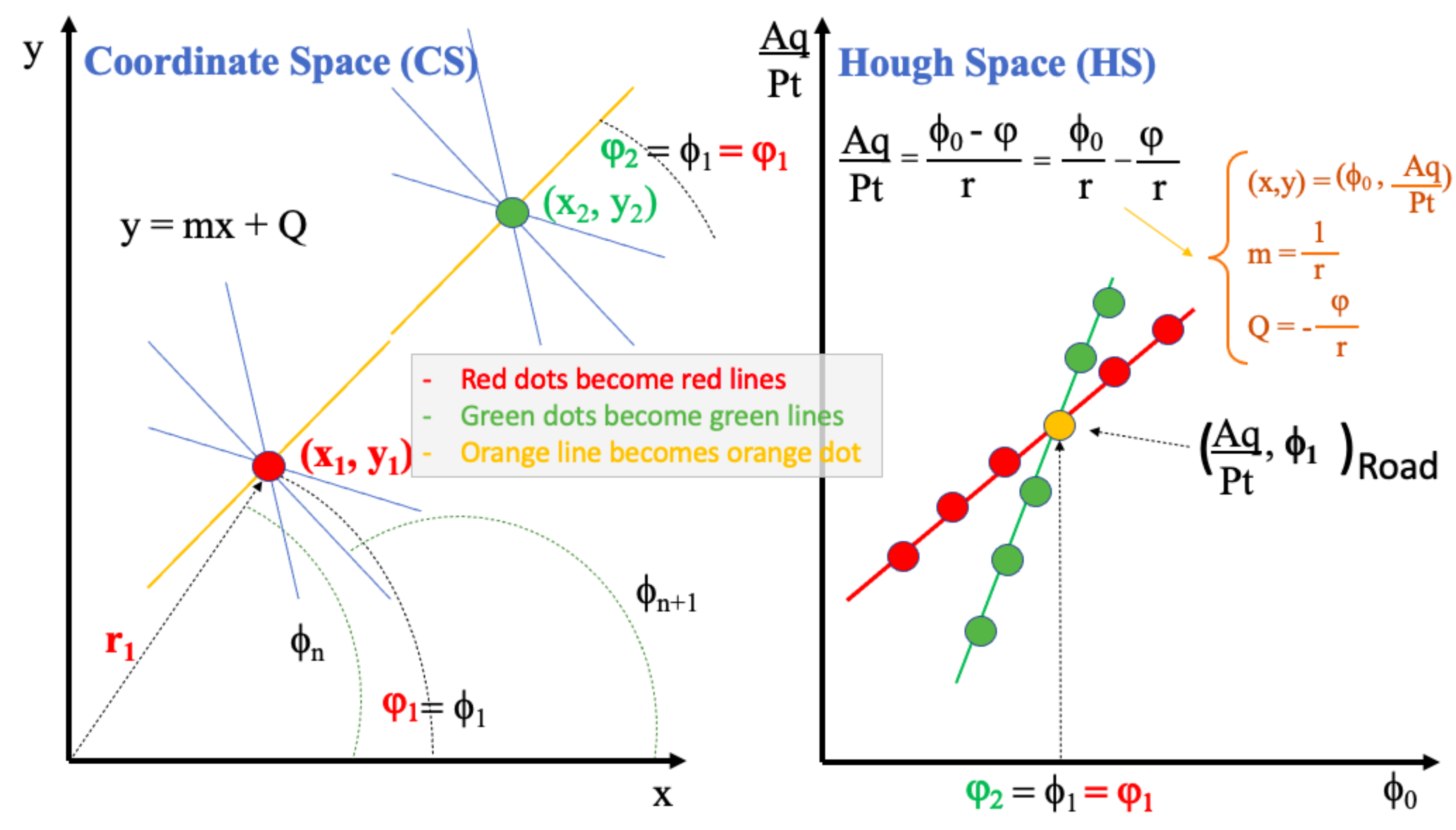
Figure 1 shows the concept: Let us imagine to have a beam of particles, moving focused clockwise and anti clockwise in an accelerator like the CERN, close to the speed of light. These particles move in opposite directions along what we define z coordinate. Then, the interaction point where these two beams collide defines not only the origin for the z coordinate but also explicits the transverse plane x, y where the products of the particle interactions are spread out in any direction. Among these, we consider only the orthogonal tracks with respect to the beam line. Hence, the new particles of interest, originated by the collisions, are studied on a bi-dimensional space that we represent as a x, y plane, orthogonal to the beam line. On this plane the trajectories represent the particle paths crossing the detectors. If the particles are charged—many of them are—and embedded in a magnetic field, they can describe a circular or helicoidal track that should be detected immediately in the Tracker, the innermost portion of the whole detector [6,7]. Left side of the Figure 1 shows this. Then, using the straight line expression:
y = m · x + Q
the line parameters can be converted in terms of slope m and intercept Q, as
m = y Q x
and the Formula (2) can be rewritten as
A q P t = ϕ 0 φ r
being r = x 2 + y 2 the radius in the Coordinate Space (CS), φ = arcsin y x the angle of the straight line with respect to the horizontal axis, again the CS, and ϕ 0 the angle at the origin of any other straight line crossing the (x, y) or ( r , ) pair. Figure 1 shows these lines with different ϕ 0 angles crossing in one point. Only one of these lines share the φ = ϕ 0 angle with the other bundle of straight lines crossing in other points. ϕ 0 [ 0 ÷ 2 π ] and A q P t are divided here in bins for histogram plots. In Formula (3), A q P t represents the particle momentum Pt in kg · m/s, the charge q in Coulomb, including a unity constant factor A that turns the units of A q P t in rad/m. The process to execute the Formula (3) for all the Hits of an input Event is here called Forward Computation.
Through this change of coordinates we move from the particle space x, y to what we call parameter or Hough Space (HS) ( A q P t , ϕ 0 ). It is shown that the straight lines in the CS turn into points in the HS. It is also shown that each point in the CS, as it can belong to an infinite bundle of straight lines, turns into a straight line in the HS. Right part of Figure 1 shows this. Hence, if we look at a given number of points in the CS that compose a straight line, as all these share the same slope and intercept, all these turn into a single point ( A q P t , ϕ 0 ) in the HS. Thus, by recognizing and extracting which points in the HS are parametrized by a given ( A q P t , ϕ 0 ) pair, we can identify which original tracks, parametrized by (x, y) or (r, ϕ) couples, are compatible with that pair. Given this concept, the HT algorithm proposed here is based on the filling the HS with a huge number of straight lines. These lines are generated, for each (r, ϕ) couple, and for each input channel, by carrying out all the possible values of the ϕ 0 angle (see below). In this way for each ϕ 0 angle inserted in the Formula (3), a correspondent momentum A q P t is calculated. Again, this is repeated for all the Hits of the input channels. It should be noted that ϕ 0 [ 0 ÷ 2 π ] and A q P t are divided here in bins for histogram plots.
In the reality, every HEP experiment deals with a given number of input-output specifications provided by software simulations. What we do here is to emulate the behaviour and performance of a physical apparatus in advance, providing all the expected physical parameters before the system is built. The main system performance is the track recognition capability, which is the number of detected tracks over the total number of expected tracks to be found. In this study the parameters that we are using to emulate a physical pattern recognition of real trajectories are summarized below.
  • Eight input data channels, originated by the Tracker.
  • The eight channels, in parallel, provide up to 500 inputs for a total number of data up to 4000 pair: These are called input Hits.
  • Each of the eight channels provides integer number for the x and y CS couples, digitized using 18 bits.
  • Each Hit is also provided on-the-fly with the CS pairs in the polar representation, besides the cartesian. The polar data are (r, ϕ) represented respectively with 12 and 16 digital bits.
  • The system is targeted to work at a clock frequency of 250 MHz.
  • For each input Hit 1200 ϕ 0 angles are created to cover the desired spread of angles in the HS (1200 bins so using 11 bits).
  • The momenta A q P t of the HT Formula (3) are binned in 64 bins, so using 6 digital bits.
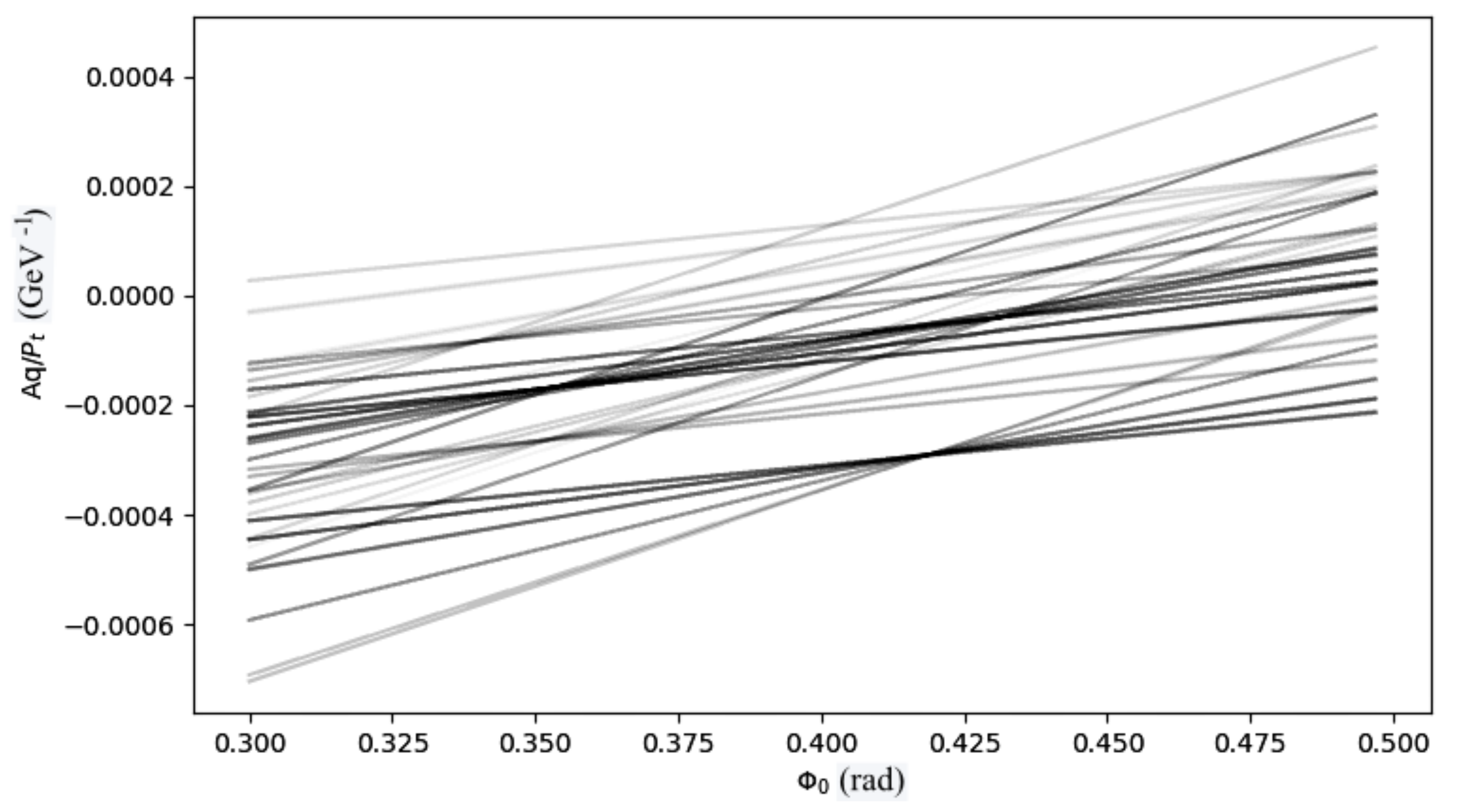
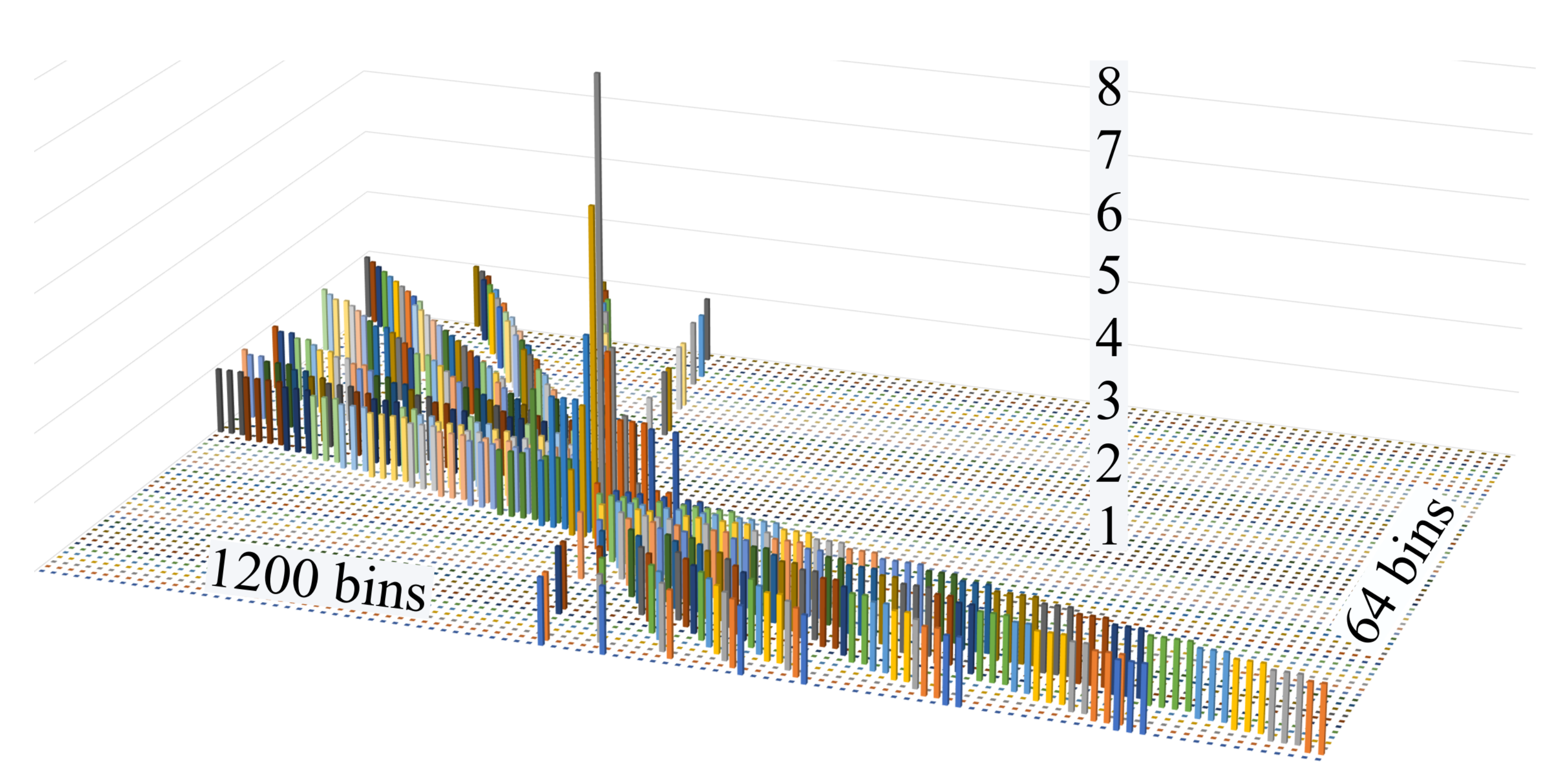
Figure 2 shows a reduced bin representation of all the tracks reconstructed using the HT Formula (3) and the consequent HS space. The hardware block that holds the HS space is called Accumulator, a 3D histogram binned horizontally along 1200 ϕ0 angles and vertically along 64 A q P t momenta. A physical Event is represented by a pair (ϕ0, A q P t ) nominated as candidate Road, (ϕ0, A q P t ) R o a d . The Accumulator is filled by applying the Hough Formula (3) to the whole set of inputs Hits (r, ϕ) pairs from the physics experiment. In particular, each pair (r, ϕ) defines a straight line in the Accumulator, drawn along the bins, as shown in Figure 2. The Accumulator can be imagined like a set of individual Towers. Figure 3 shows an example of a 3D picture of the Accumulator filled up with many straight lines crossing in a (ϕ0, A q P t ) R o a d . In this example the Road is the only Tower 8 high.
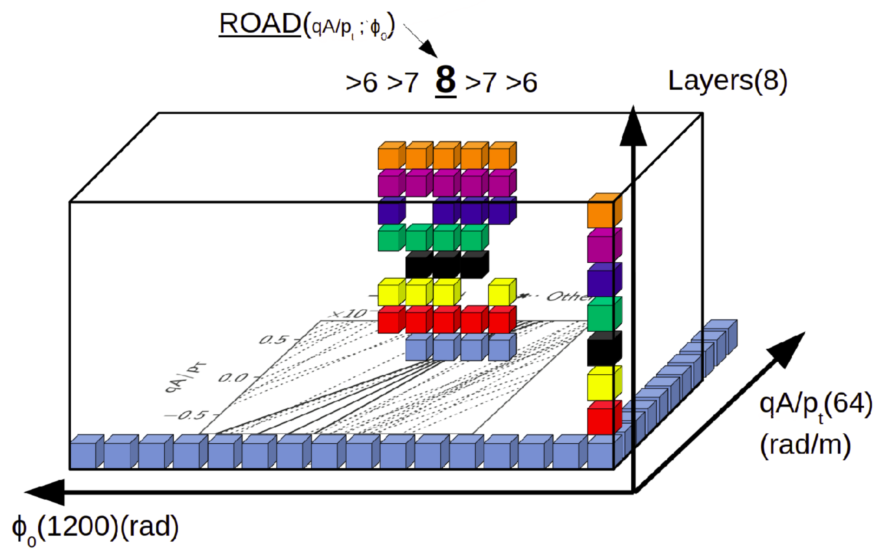
Each Tower is composed of eight elements (indicized with n) that hold the information of whether that Tower has been touched at least by one line originated by the n-th input channel.
For example, if a Hit belonging to the 5th input channel generates through the HT Formula (3) a line crossing the Accumulator and passing through the n-th row, m-th column, the Tower identified at n-th row (representing one of the 64 A q P t ) and the m-th column (representing one of the 1200 ϕ0) is updated with a “1” in its 5th floor. This is done for all the Towers touched by that straight lines. This is shown in the Figure 4 using colored cubes. Each colour, in fact, represents a layer/input channel (floor).
In the Figure 4 the numbers 6, 7, 8, 7, 6 mean that, in this case, a Road is detected when adjacent Towers of the Accumulator contribute with these numbers to the sequence of counts, hence there is a sequence of Towers 6, 7, 8, 7, 6 high.

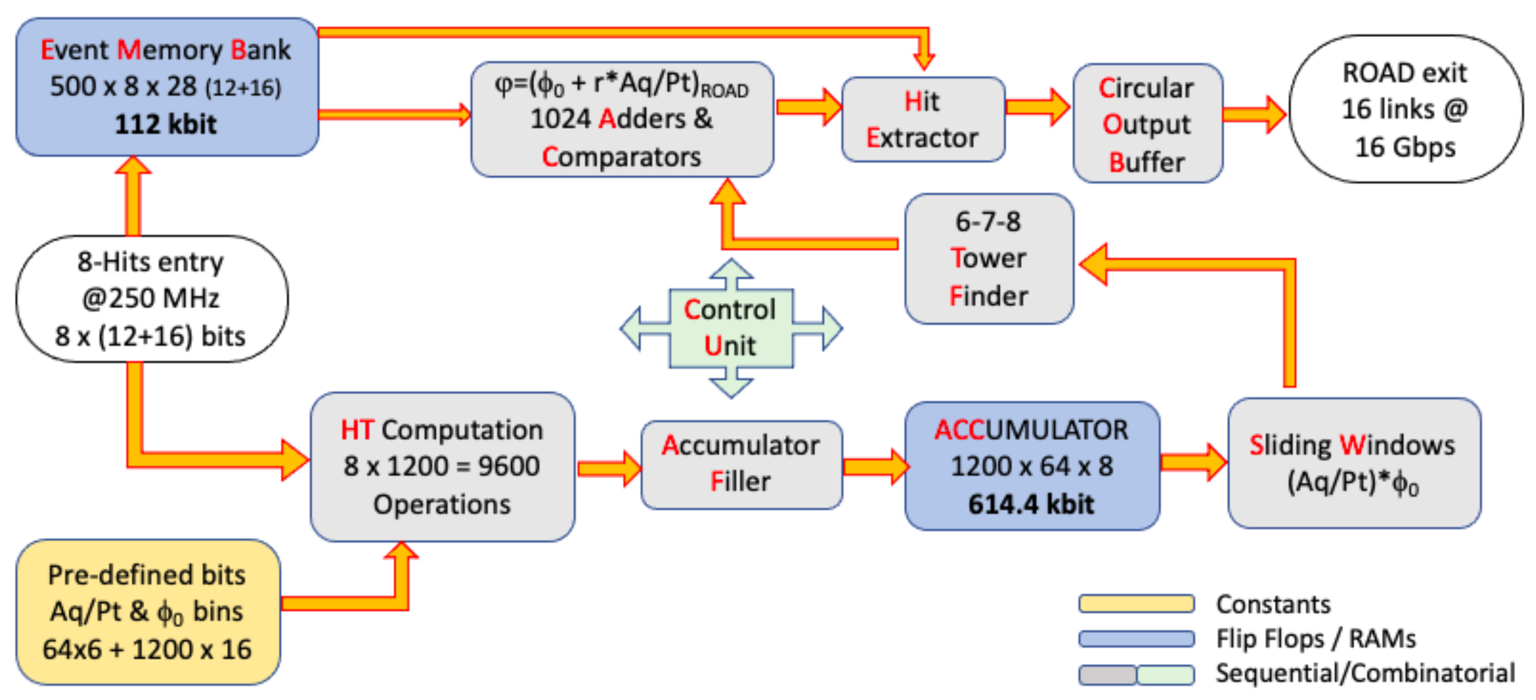
3. Block Diagram of the HT Implementation on FPGA

Figure 5 shows how the HT algorithm has been divided in logic blocks, as they have been separately designed following the firmware (FM) functional description. We did not design the inner blocks with a further nested structure, hence each block is here presented with a behavioural description only. We have used a low-level of abstraction approach for the FM development, so not using predefined vendor macro blocks and with no high-level synthesis [10]. We wanted a FM description at the level of the individual components, simulating the VHDL code in steps. First, the behavioural code was simulated block by block to make sure the functionality of the system was correct. Then, after synthesizing and extracting the parasitics from the netlist we run post-synthesis simulations and, finally, the same approach was used to run post-layout simulations to include all the parasitics extracted after the layout was produced. The post-synthesis and post-layout simulations were used mainly to find the limits of operation of the entire circuits in terms of maximum clock frequency, input to output latency and area occupation on the FPGA. Moreover, we were able to tune the synthesis and layout steps to better optimize the critical nets and bottlenecks of the system.
Let us summarize briefly the scope of each block of the diagram, after the eight Hits enter the system (see first left block in the Figure 5). As a caption for the figure, the circuits based on flip-flops are blue blocks, yellow blocks refer to predefined constant valued that can be hardwired to logic “0” s and “1” s and can be modified with a new synthesis of the blocks. For some blocks the latency was a compromise between introducing digital pipelines [11] to speed up the circuit and the need to reduce the area occupied in the FPGA layout.
The input data enter in parallel two blocks: The Event Memory Bank and the HT computation.

3.1. Event Memory Bank

This is a bank of Flip-Flops and internal RAM memories used to save the entire set of Hits that compose one Event. Its size is dimensioned depending on the number of input channels, Hits and on the number of bits used to represent the data.

3.2. HT Computation

This HT Computation circuit carries out the Formula (3) in parallel for the eight inputs and for the 1200 bins, performing 9600 operations every clock period. It generates all the A q P t points that compose all the 9600 straight lines. The FW for this circuit is synthesized in Look Up Tables (LUTs) as far as the additions/subtractions and in Digital Signal Processing (DSPs) for multiplications/divisions.

3.3. Accumulator Filler

This circuit updates the Accumulator, once all the A q P t points are calculated from the Formula (3) for all the inputs, by saving “1” s in the proper positions of the Towers. This is implemented with LUTs only.

3.4. Accumulator

This is a Flop-Flop based memory, composed of 8-element Towers accounting for the HS. The Accumulator size is defined by the (ϕ0, A q P t ) bin numbers. For our study we have investigated the 1200 × 64 size because these have been found as largest numbers compatible with the resources of the FPGA. However, some smaller configurations have also been studied, for not launching too long processing times, and are shown in the next sections.

Accumulator Sectors

A strategy to reduce greatly the FPGA resource utilization is what we call Sector method. To better share the available electronics components within the FPGA, the HT Formula (3) is applied in parallel to two different types of data. In more detail, r and ϕ are fixed values while ϕ0 increases linearly in steps. This can be expressed via the Formula:
( A q P t ) n = ϕ 0 ( n 1 ) φ r + Δ ϕ 0 r
being ϕ 0 n = Δ ϕ 0 · n , with n [ 0 ; 1200 ] and Δ ϕ 0 is the constant width of the ϕ 0 bins. Here ϕ 0 0 is the angle of the first bin. In other words we calculate the A q P t value for the first bin then we reitarate n times an addition of a constant value expressing the horizontal step Δ ϕ 0 of the line. The Accumulator is hence divided in Sectors of equal ranges alongside ϕ 0. By applying this strategy we reduce the computational logic as we need only mathematical sums to carry out the multiplications Δ ϕ 0 r . This circuit is implemented using DSPs to calculate the division in the first bin, then all the other sectors are implemented using LUTs only, as these are carried out with additions. In any case all these computations are executed in parallel.

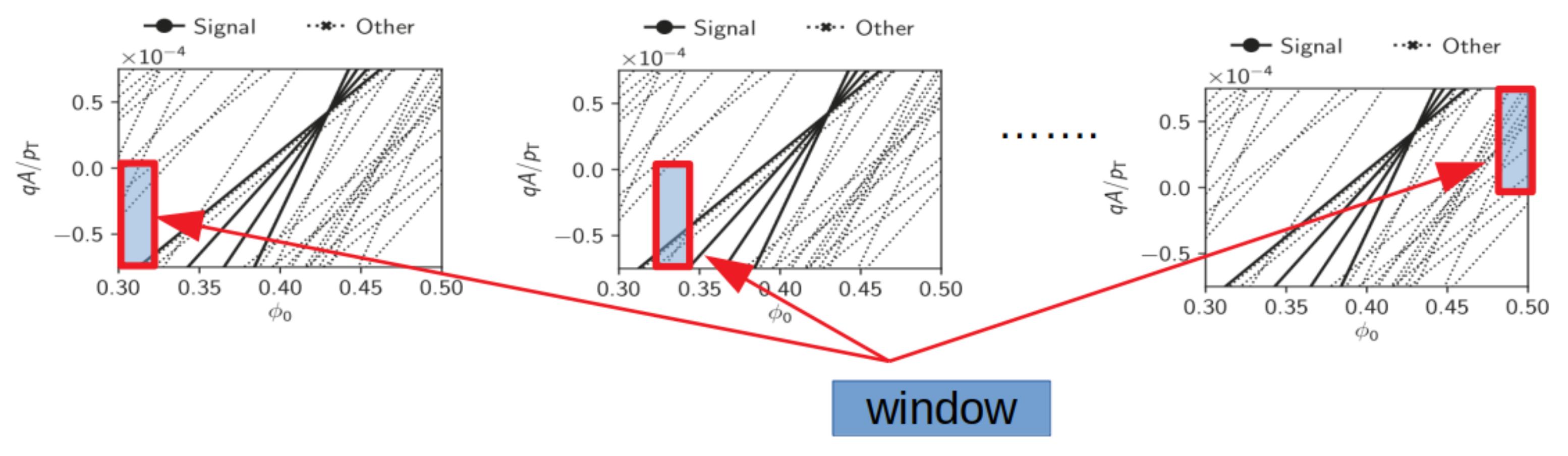
3.5. Sliding Windows

As the Accumulator becomes easily too big to be processed within one clock period, to identify all the candidate Roads, it is scanned in successive smaller windows, one at a time. Of course, the greater the number of the windows, the smaller the circuit at the expense of a longer latency. This circuit is synthesized using LUTs only.

3.6. Tower Finder

This circuits sets, for each Tower of the Accumulator, a couple of bits to identify if the number of “1” s in the Tower is lower than 6, 6, 7 or 8. Hence, the system is ready to start finding the Roads as candidate tracks. As described above, the sequence of 6, 7, 8, 7, 6 is the minimum set of heights, in adjacent Towers, representing a Roads candidate. This circuit is synthesized using LUTs only.

3.7. Adders and Comparators

This circuit compares the Roads which have been found, in terms of ( ϕ 0, A q P t ) R o a d coordinates, with all the (r, ϕ) input compatible Hts that were saved into the Event Memory Bank. This compatibility is asserted by performing the HT Formula (3), in a reverse manner. In fact this process, namely the Backward Computation, carries out the mathematical expression:
( A q P t ) R o a d A q P t = ( A q P t ) R o a d ( ϕ 0 R o a d φ r )
In other terms we insert the ϕ 0 R o a d and the Hit numbers (r, ϕ) in the Formula (3), so we extract the A q P t value and compare it to the A q P t R o a d . This process is done in parallel for the entire Event composed of the 4000 Hits saved in the Event Memory Bank. This circuit is synthezized in DSPs for the divisions and LUTs for the additions.

3.8. Hit Extractor

This circuit, depending on the result of the Backward Computation HT Formula (5), hence depending on the difference ( A q P t ) R o a d A q P t has the capability to accept or reject the Hit coordinates (r, ϕ) as Hit candidates for that Road. This circuit is synthesized using LUTs only.

3.9. Circular Output Buffer

This simply put all the extracted Hits, once have passed the previous selection, in a circular FIFO memory to be sent to output. This component is connected to a certain number of UltraScale+ GTH (16.3 Gb/s) transceivers [12] of the FPGA, with a frequency targeted up to 250 MHz. The Aurora 64b/66b [13] data encoding protocol has been chosen as standard protocol. This circuit is synthesized using First In Fisrt Out circuits (FIFOs), i.e., Flip-Flops.

4. Firmware Design

In this project we have used FPGAs and we have designed a firmware (FW) starting from a low abstraction level of description, without using high-level synthesizers or other compilers targeted to other types of programmable devices because such a huge system would not fit, converging with the same performance. In addition, it should be noted that using other programmable devices as GPUs or CPUs instead of FPGAs we would not be able to guarantee a fixed latency, as estimated below, and this is a need for HEP experiments. Hence, the FW design is focused on Formula (3) which generates the straight lines in the HS Accumulator starting from the physical Hits (r, ϕ) of the input Event. Figure 6 shows how the FW has been segmented to optimize the synthesis process.
We use an example to describe a case of tracks coming from a 8-layer detector and an Accumulator composed of 1200 ϕ0· 64 A q P t bins according to simulations that validate these numbers to fit the required detection efficiency.
Figure 7 shows the Sliding Window process for the selection of a small section (window) of the Accumulator. This is scanned to identify for the Roads, in successive steps and as this process is a recursive parallel task to share FPGA electronics components. In parallel with the Road extraction the Backward Computation task is performed by running again the Hough Formula (5) for all the input Hits saved in the Event Memory Bank. Only those Hits that match the Formula (5) are extracted and sent out after being queued in the Circular Output Buffer.

FW Synthesis and Place & Route

We have configured the Block Diagram of Figure 5 to optimize the HT algorithm synthesis on the Alveo U250 Xilinx UltraScale+ FPGA device to push a parallel implementation on the electronics resources (CLBs/LUTs, RAMs, DSPs). This is why the Accumulator is scanned via logic Sliding Windows that use a parallel implementation of the Accumulator Sectors. In addition, the synthesis Timing Constraint matching has been achieved by individual management of internal critical circuits paths. Figure 8 shows a pictorial example of the layout of the entire HT algorithm. In this example eight clock trees have been used separately as they are asynchronous: These are partially emphasized in different colours.
The main basic rules for matching the Timing Constraints during the synthesis refer to the Flip Flops Hold and Setup times which must be respected. In particular, if the Setup time is somewhere not fulfilled, in general, the problem can be fixed by reducing the clock frequency, when this is possible. By contrast, if what is not fulfilled is the Hold-Time and the synthesis process reports Hold-Time Violations, the circuit will not work at any frequency at all. This is why we put a particular effort to cure the description of the critical nets, starting from the VHDL code, and we have provided Timing Constraints in terms of Hold-Time and Max-FanOut before running the synthesis. We also reduced the number of LUTs among the Flip Flops sharing the same state machine, by adding pipeline stages so to facilitate the Place and Route efficiency. In addition, we have separated the main complex logic functions, those with high-input/low-output numbers by implementing different logic circuits and paths, by using Register Transfer Logic (RTL) VHDL description. Moreover, the management of the Super Logic Regions (SLR) [14] in the Virtex UltraScale+ FPGA has been evaluated as a crucial step to be applied for driving the logic blocks to specific layout locations. In fact, it is obvious that interconnections between different SLRs are slower that those within an individual SLR. For this reason we avoided implementing high-speed critical nets, dense and fast buses in different SLRs. For example, we have adopted this strategy in the data transmission with Dual Clock FIFOs, which are FPGA internal programmable COREs allowing to connect two different clock domains. The FW in fact, as it has been designed and constrained exploiting eight clock domains, left the Place and Route tool the freedom to choose the best compromise to match the Timing Constraints without excessively expanding the network. Table 1 summarizes some implementation numbers that have been chosen for making performance comparisons. It is shown how the use of SLRs affects the system performance. In particular, these numbers refer a different use case of FW implementation. In fact, by reducing the Accumulator binning in terms of ( A q P t , ϕ 0 ) the overall synthesis and Place and Route can better adapt to match the constraints. All tested examples have been implemented using the Alveo U250 device. Failed nets in the Table 1 indicate the nets that, after the Place and Route task do not match the Setup Time. By violating the Setup Time the circuit can again work, as long as the clock speed is reduced, or as long as these nets are routed again.
The maximum achievable frequency, shown with Formula (6), has been estimated by following the XILINX user guide [12,14] and validated by the post-layout simulations, those most accurate simulations carried out by including the parasitic parameters extracted after the design is closed. In fact, the Worst Negative Slack (WNS) for the Setup time extracted in the synthesis routing report lead us to estimate a:
M a x F r e q u e n c y = 1000 T c l o c k W N S MHz = 1000 4 + 0.5 ns MHz = 222.2 MHz
We can also give an estimation of the total input ITT and output OTT maximum throughput, shown with Formulas (7) and (8). In particular, the ITT is the data stream per second which enter the system: Eight channels load one Hit per clock period and each Hit (r, φ) is composed of 12 + 16 = 28 bits.
I T T ( B y t e s ) = 8 · 28 · 250 MHz 8 bit = 7 GBps
As far as the output OTT throughput we consider 16 output transceivers which run up to 16 GBps each, using the Aurora encoding. Once a Road has been identified along with all the original input Hits that have generated it, these Hits, which are still composed of 28 bits, must be sent out in parallel via the 16 output transceivers. Consequently, the OTT is given by:
O T T ( B y t e s ) = 16 · 28 · 250 MHz 8 bit = 14 GBps
It is shown that in this way, as the OTT is larger that the IT and we use an internal queueing technique based on the Circular Output Buffer, the entire system can stand the input data stream. In this example, the total Latency of the circuit presented in Figure 5 is 30 clock periods. The total processing time associated to an Event depends on the #Hits, on the Latency, on the #Roads and naturally on the clock frequency, where:
  • #Hits is the total number of input data (Hits) loaded eight at a time;
  • #Roads is the total number of identified Roads within a given Event;
  • Latency is the number of clock periods from when the entire Event is loaded to when the first set of Hits belonging to the first Road is sent out.
Table 2 shows as example the internal resources used to implement the design into the Alveo U250 platform. In fact, to understand how the Accumulator binning scales with the resource occupancy we have made different implementations and the results proof that the HT system as we propose can fit a commercial frontier FPGA. The number of transceivers, 24 in the Alveo U250, are fully used to input eight channels and output 16 parallel data streams after the Circular Outpout Buffer in Figure 5.

5. Conclusions

The paper presents an implementation study of the Hough transform algorithm on a physical FPGA. The Xilinx UltraScale+ family has been chosen as target devices, in particular the Alveo U250 FPGA. The study started with a firmware specification composed of 60 ϕ 0 angles, a target clock frequency of 250 MHz, 4000 input Hits acquired in parallel on eight channels in 500 clock periods, an Acccumulator swept using 40 Sliding Windows and 20 Accumulator Sectors. The use of FPGAs in this context is driven by the necessity to reduce data on-the fly during a data acquisition process. For this, FPGA components, if compared to other programmable devices, can provide at the same time a low and fixed latency, low power consumption and high throughput and data rate. In this way high-energy physics experiments can reduce the acquired data flow from one to two orders of magnitude. In addition, a huge simulation work has been prepared to validate the firmware: The current status of the Hough transform firmware design is complete at the RTL abstraction level, synthesizable and we can simulate the whole VHDL code behaviour. Then, post synthesis and post layout simulations are also available by adding the parasitic capacitances related to the physical wires and components of the FPGA internal interconnections. Moreover, a Python based development tool has been created to emulate the firmware algorithm to test its behaviour on dummy data. Dummy Roads have been generated within a set of dummy input Hits to simulate the efficiency performance of the entire architecture at finding candidate tracks among the input data stream. This study of possible implementations of the Hough transform algorithms on high-energy physics experiments in not new but, in particular for particle recognition in hardware tracking systems, has converged to a physical FPGA implementation for the first time. In fact, up to now, the Hough transform in high-energy physics experiments has only been implemented using software-based systems.

Author Contributions

Conceptualization, A.G., A.A. and A.C. (Alessandro Cerri); Investigation, F.A. and A.C. (Alessandra Camplani); Methodology, A.C. (Alessandro Cerri); Resources, A.C. (Alessandro Cerri); Supervision, A.G., A.A. and A.C. (Alessandro Cerri); Validation, F.A. and A.C. (Alessandra Camplani). All authors have read and agreed to the published version of the manuscript.

Funding

This research received no external funding.

Acknowledgments

The authors acknowledge the support of INFN, Niels Bohr Institute of Copenhagen University, STFC and the University of Sussex.

Conflicts of Interest

The authors declare no conflict of interest.

References

  1. Apollinari, G.; Béjar Alonso, I.; Brüning, O.; Fessia, P.; Lamont, M.; Rossi, L.; Tavian, L. High-Luminosity Large Hadron Collider (HL-LHC): Technical Design Report V. 0.1; CERN Yellow Report Monographs CERN-2017-007-M; CERN: Geneva, Switzerland, 2017; Volume 4, p. 599. [Google Scholar]
  2. Perkins, D.H. Introduction to High Energy Physics; Cambridge University Press: Cambridge, UK, 2000. [Google Scholar]
  3. Ryd, A.; Skinnari, L. Tracking Triggers for the HL-LHC. Annu. Rev. Nucl. Part. Sci. 2020, 70, 171–195. [Google Scholar] [CrossRef]
  4. Hassanein, A.S.; Mohammad, S.; Sameer, M.; Ragab, M.E. A survey on Hough Transform, Theory, Techniques and Applications. Int. J. Comput. Sci. 2015, 12, 32–58. [Google Scholar]
  5. Mukhopadhyay, P.; Chaudhuria, B.B. A survey of Hough Transform. Pattern Recognit. 2015, 48, 993–1010. [Google Scholar] [CrossRef]
  6. Abeling, K. Expected tracking performance with the HL-LHC ATLAS detector. In Proceedings of the Science PoS(EPS-HEP2019)177, Ghent, Belgium, 10–17 July 2019; Volume 364. [Google Scholar]
  7. La Rosa, A. The Upgrade of the CMS Tracker at HL-LHC. JPS Conf. Proc. 2021, 34, 010006. [Google Scholar]
  8. Ramesh, N.; Purdy, G.; Purdy, C.; Smith, J. A Hardware Implementation of Hough Transform Based on Parabolic Duality. In Proceedings of the IEEE 57th Int. Midwest Sym. on Circuits and Systems (MWSCAS), College Station, TX, USA, 3–6 August 2014; pp. 145–148. [Google Scholar]
  9. Ralston, J.; Ngo, H. Design of an embedded system for real-time lane detection based on the linear Hough transform. In Proceedings of the SPIE 11736, Real-Time Image Processing and Deep Learning, Online, 12–16 April 2021; Volume 11736. [Google Scholar] [CrossRef]
  10. Baranov, S. High Level Synthesis of Digital Systems: For Data Path and Control Dominated Systems; ACM Digital Library: Ottawa, ON, Canada, 2018; p. 207. ISBN 978-1-7750917-1-4. [Google Scholar]
  11. Zhang, J.; Ma, J.; Yan, Z. Identification of Pipeline Circuit Design. Electron. Signal Process. 2015, 97, 71–76. [Google Scholar]
  12. Xilinx, UltraScale and UltraScale+ GTY Transceivers. UltraScale Architecture GTY Transceivers UG578. 2017, p. 446. Available online: https://www.xilinx.com/support/documentation/user\char_guides/ug578-ultrascale-gty-transceivers.pdf (accessed on 15 October 2021).
  13. Xilinx, Aurora 64B/66B v12.0 LogiCORE IP Product Guide. Vivado Design Suite PG074. 2020, p. 145. Available online: https://www.xilinx.com/support/documentation/ip\char_documentation/aurora\char_64b66b/v11\char_2/pg074-aurora-64b66b.pdf (accessed on 15 October 2021).
  14. Xilinx, UltraFast DesignMethodology Guide forXilinx FPGAs and SoCs. UG949 (v2021.1). 2020, p. 327. Available online: https://www.xilinx.com/support/documentation/sw\char_manuals/xilinx2020\char_1/ug949-vivado-design-methodology.pdf (accessed on 15 October 2021).
Figure 1. Example of Hough transform based on the straight line formula y = x · m + Q. The plot on the left shows the Coordinate Space, the right plot the Hough Space.
Electronics 10 02546 g001
Figure 2. Hough Space after executing HT Formula (3): Example with electron-Volt eV and charge q set to 1 units.
Electronics 10 02546 g002
Figure 3. 3D plot of the Hough Space after executing the HT Formula (3).
Electronics 10 02546 g003
Figure 4. 3D view of the Accumulator with a candidate Road.
Electronics 10 02546 g004
Figure 5. Block diagram of the Hough transform algorithm implemented in FPGA.
Electronics 10 02546 g005
Figure 6. Overview of the HT firmware logic.
Electronics 10 02546 g006
Figure 7. The Sliding Windows approach: The red rectangles are scanned along the Accumulator.
Electronics 10 02546 g007
Figure 8. Critical paths management in the FW. The logic has been divided and placed in different Super Logic Regions depending on the clock trees (different colours in the Figure).
Electronics 10 02546 g008
Table 1. Examples of FW implementation after the Place and Route.
DeviceFirmware VersionSetup
WNS (ns)
Failed Nets/Total NetsMax Freq./
Targeted Freq.
(MHz)
Development
Strategy
Alveo
U250
Accumulator 216 qA/Pt by
64 ϕ 0 , 800 hits
−0.6734000/610,000214/250Without SLRs
Alveo
U250
Accumulator 222 qA/Pt by
72 ϕ 0 , 800 hits
−0.2544200/795,000235/250With SLRs
Alveo
U250
Accumulator 216 qA/Pt by
216 ϕ 0 , 800 hits
−3.776104,000/1,582,000128/250Without SLRs
Alveo
U250
Accumulator 222 qA/Pt by
224 ϕ 0 , 800 hits
−0.44152/1,769,000225/250With SLRs
Table 2. Alveo U250 resources as from the Place and Route task.
DeviceFirmware VersionFlip
Flops
(%)
Look-Up
Table (%)
Digital
Signal
Processor (%)
GigaBit
Transceivers
IO (%)
Block
RAM
Memory
(%)
Alveo U250Accumulator 216 qA/Pt
by 64 ϕ 0 , 800 hits
91781001
Alveo U250Accumulator 222 qA/Pt
by 72 ϕ 0 , 800 hits
111981001
Alveo U250Accumulator 216 qA/Pt
by 216 ϕ 0 , 800 hits
2452121001
Alveo U250Accumulator 222 qA/Pt
by 224 ϕ 0 , 800 hits
2853121003
Publisher’s Note: MDPI stays neutral with regard to jurisdictional claims in published maps and institutional affiliations.

