
HTNURL: Design of a High-Performance Low-Cost Triple-Node Upset Self-Recoverable Latch


Abstract
:1. Introduction
2. Typical Radiation Hardened Designs
2.1. LCHRNAN
2.2. HRPU
2.3. DNCS
2.4. Delta DICE
2.5. TNUHL
2.6. LCTNURL
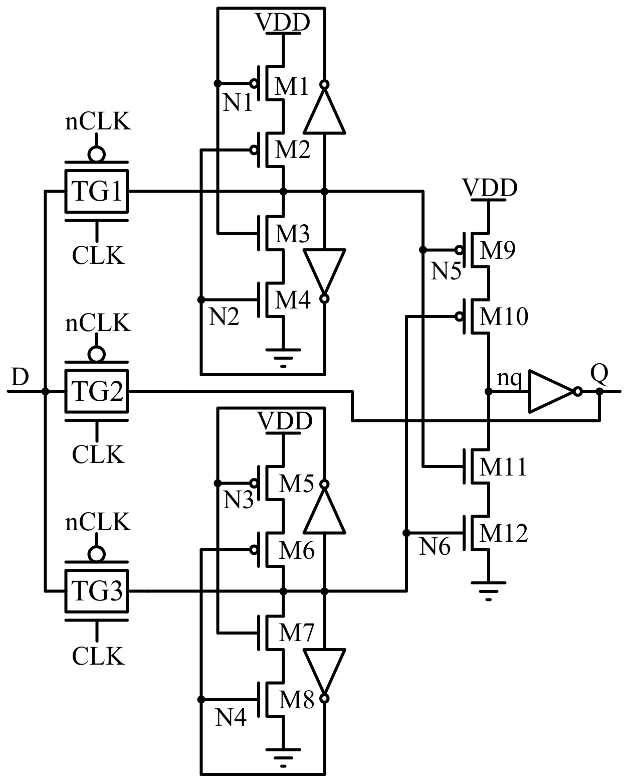
2.7. TNURL
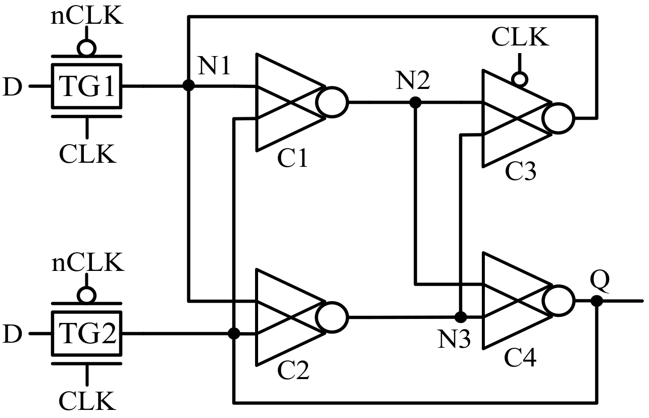
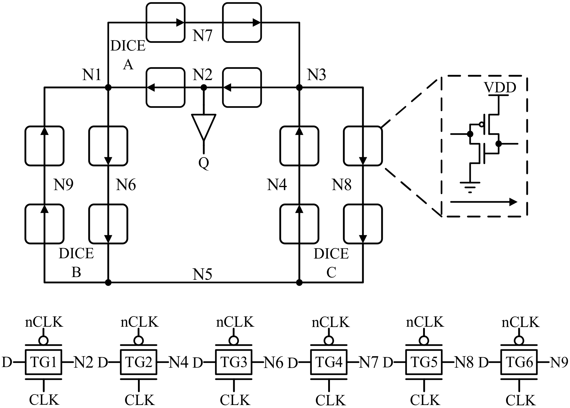
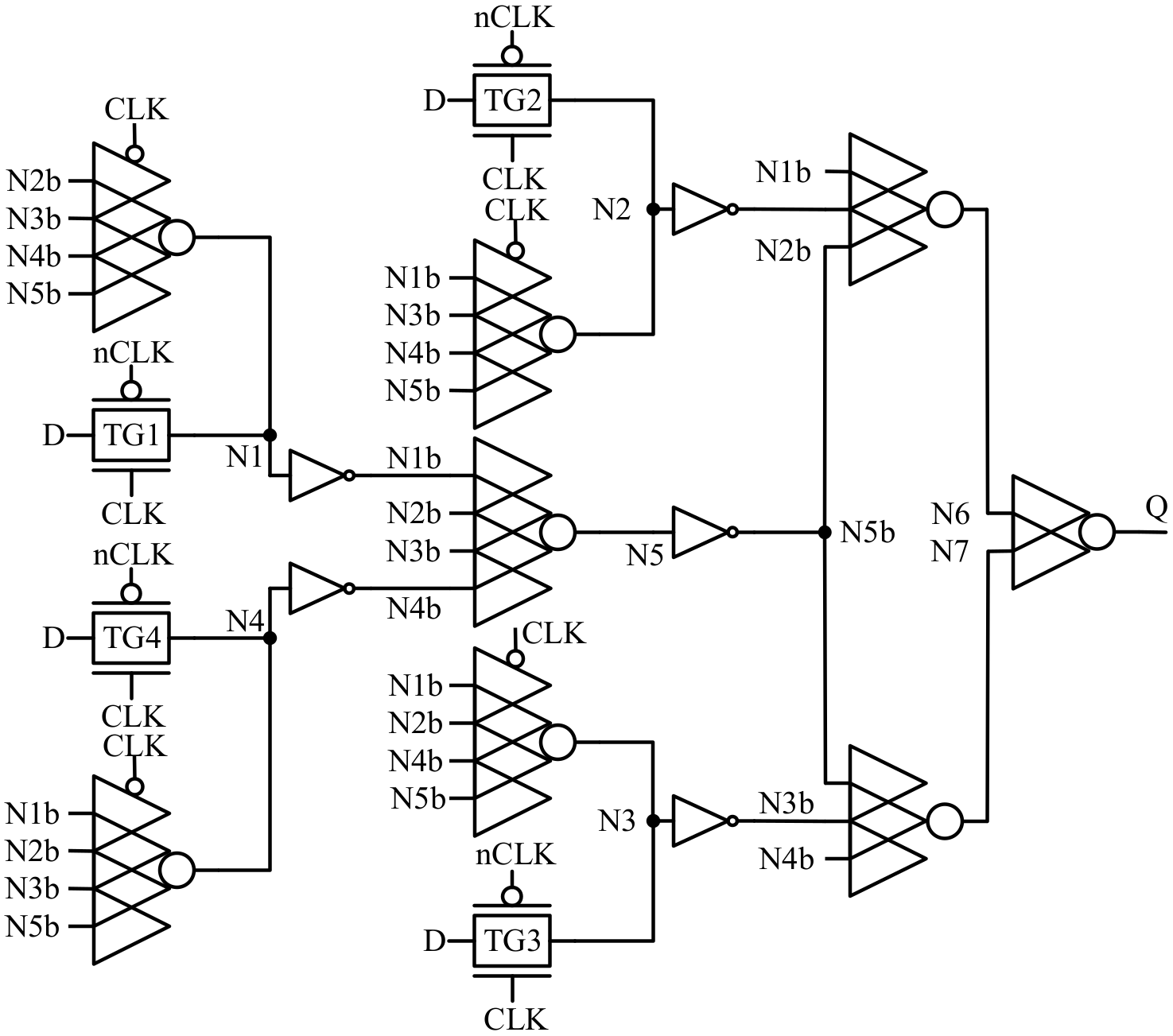
3. Proposed Hardened Latch Design
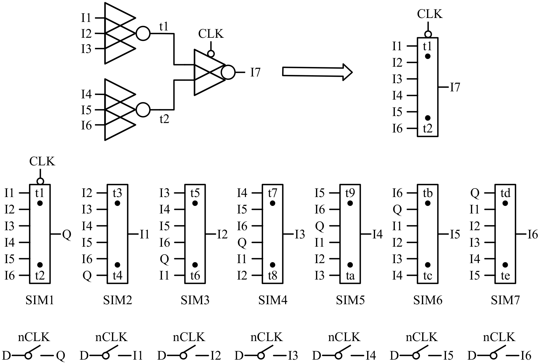
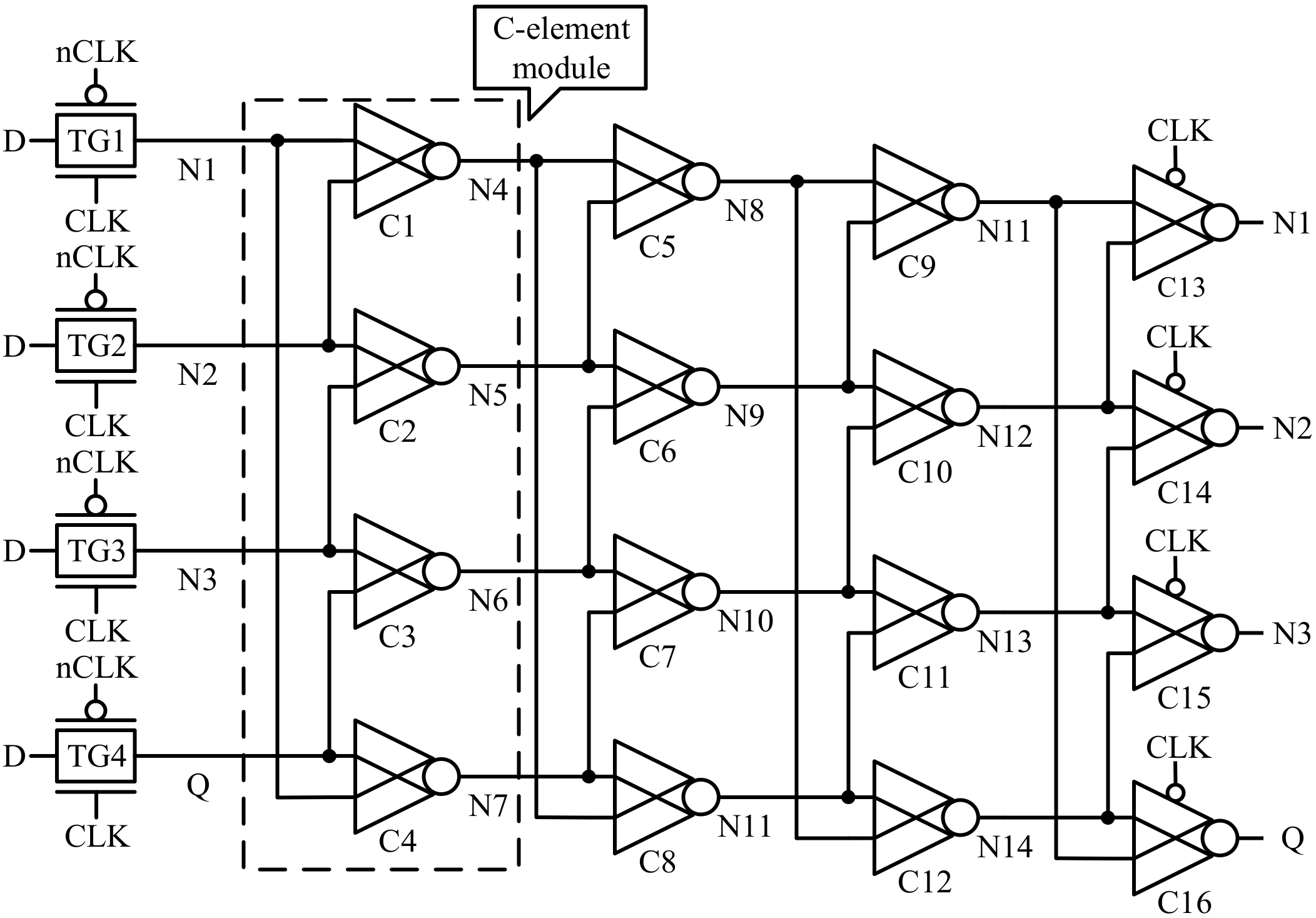
3.1. Circuit Design and Behavior
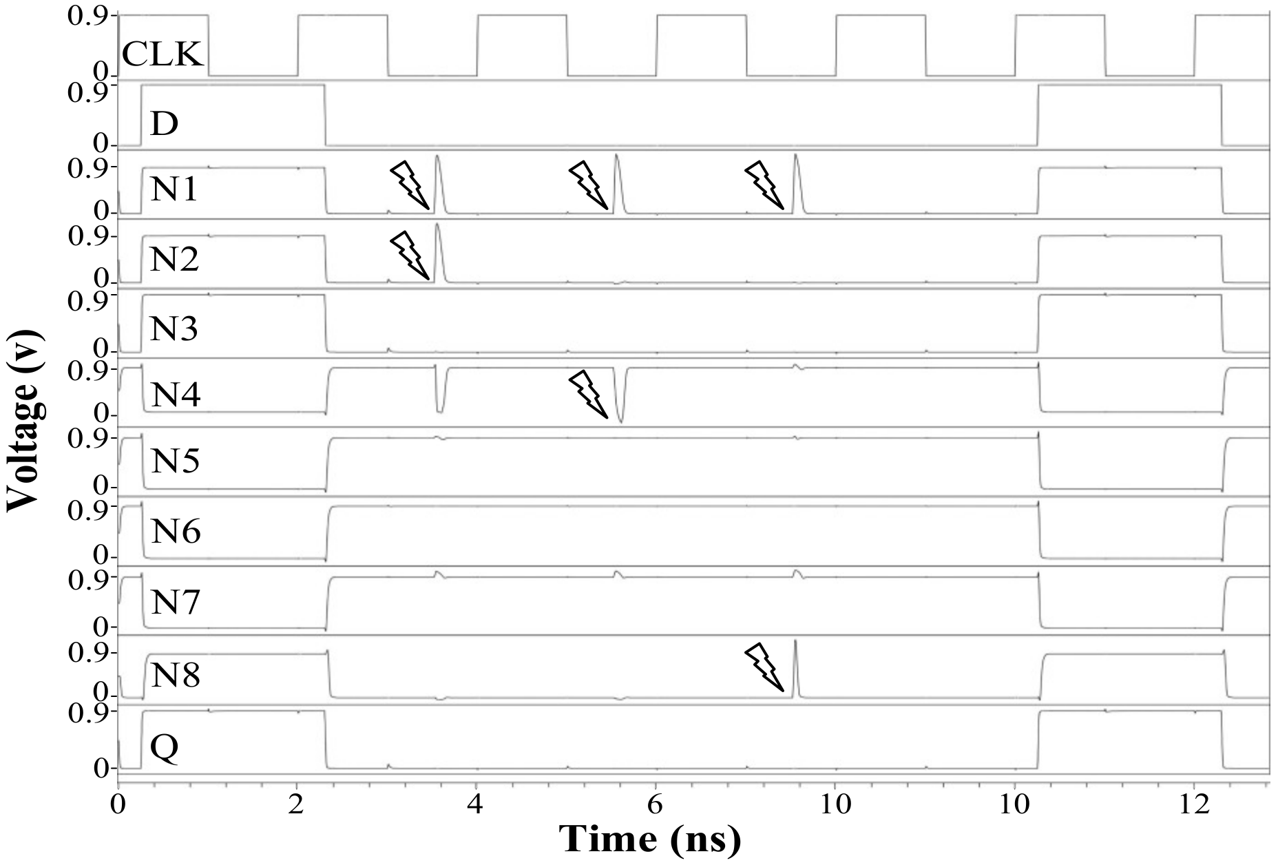
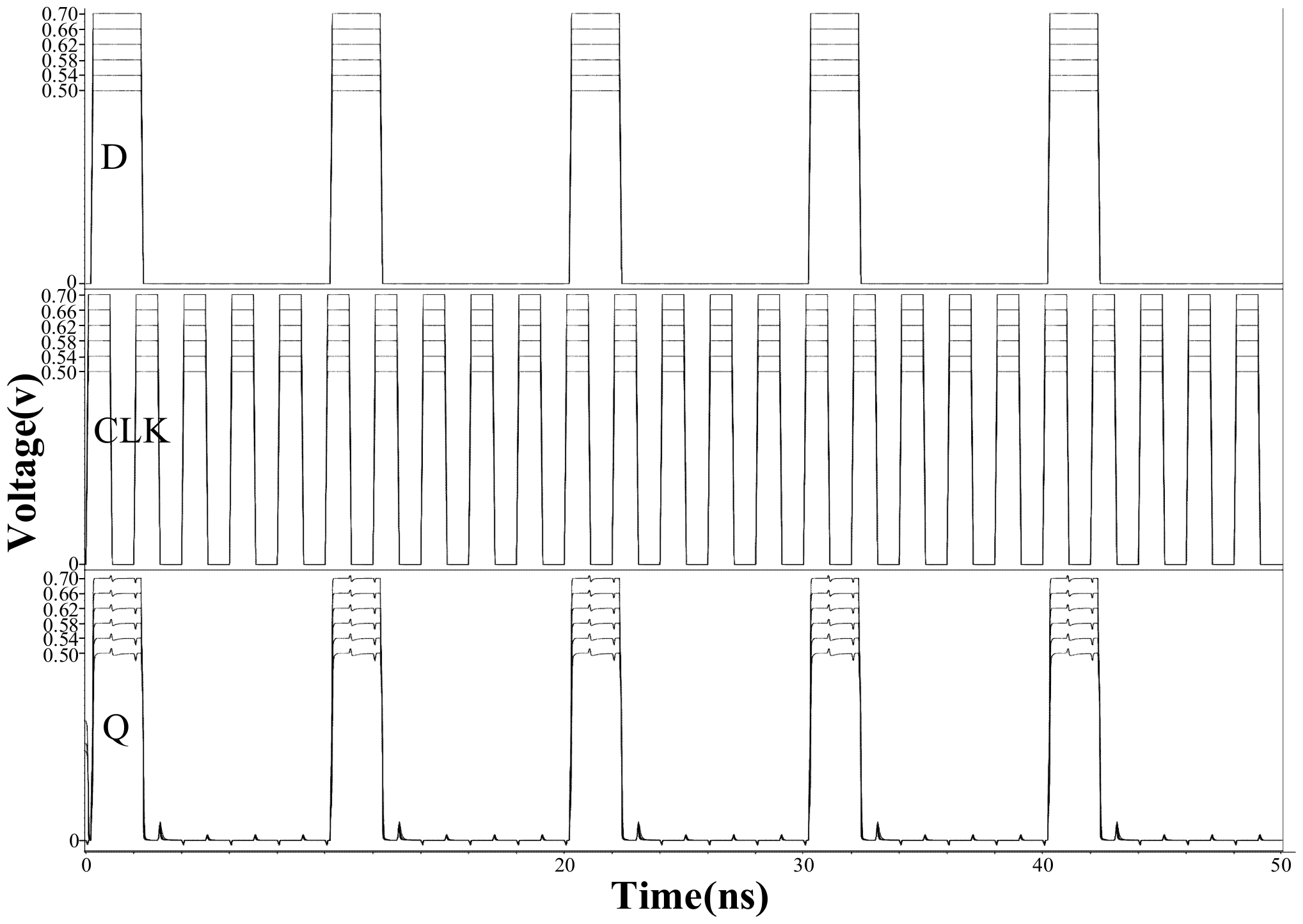
3.2. Verification Results
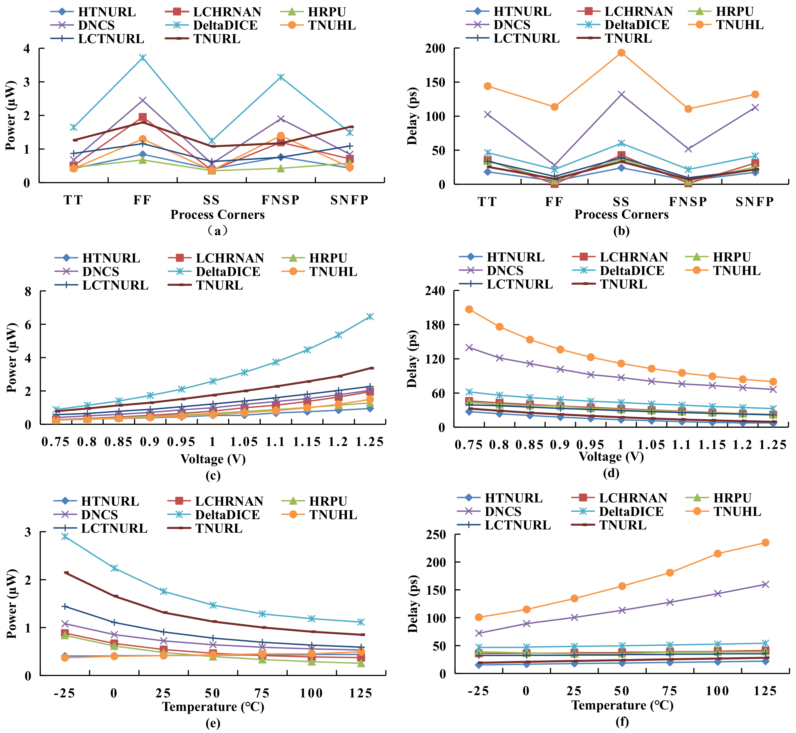
4. Comparisons and Evaluation
4.1. Performance Evaluation
4.2. Effect of PVT Variations on Latches
5. Conclusion and Future Work
Author Contributions
Funding
Conflicts of Interest
References
- Xu, H.; Zhu, J.; Lu, X.; Li, J. An advanced SEU tolerant latch based on error detection. J. Semicond. 2018, 39, 81–84. [Google Scholar] [CrossRef]
- Yan, A.; Lai, C.; Zhang, Y.; Cui, J.; Huang, Z.; Song, J.; Guo, J.; Wen, X. Novel Low Cost, Double-and-Triple-Node-Upset-Tolerant Latch Designs for Nano-scale CMOS. IEEE Trans. Emerg. Top. Comput. 2021, 9, 520–533. [Google Scholar] [CrossRef] [Green Version]
- Yan, A.; Ling, Y.; Cui, J.; Chen, Z.; Huang, Z.; Song, J.; Girard, P.; Wen, X. Quadruple Cross-Coupled Dual-Interlocked-Storage-Cells-Based Multiple-Node-Upset-Tolerant Latch Designs. IEEE Trans. Circuits Syst. I Regul. Pap. 2020, 67, 879–890. [Google Scholar] [CrossRef]
- Yan, A.; Feng, X.; Hu, Y.; Lai, C.; Cui, J.; Chen, Z.; Miyase, K.; Wen, X. Design of a Triple-Node-Upset Self-Recoverable Latch for Aerospace Applications in Harsh Radiation Environments. IEEE Trans. Aerosp. Electron. Syst. 2020, 56, 1163–1171. [Google Scholar] [CrossRef]
- Yan, A.; Xu, Z.; Yang, K.; Cui, J.; Huang, Z.; Girard, P.; Wen, X. A Novel Low-Cost TMR-Without-Voter Based HIS-Insensitive and MNU-Tolerant Latch Design for Aerospace Applications. IEEE Trans. Aerosp. Electron. Syst. 2020, 56, 2666–2676. [Google Scholar] [CrossRef]
- Kumar, C.; Anand, B. A Highly Reliable and Energy Efficient Triple-Node-Upset Tolerant Latch Design. IEEE Trans. Nucl. Sci. 2019, 66, 2196–2206. [Google Scholar] [CrossRef]
- Song, Z.; Yan, A.; Cui, J.; Chen, Z.; Li, X.; Wen, X.; Lai, C.; Huang, Z.; Liang, H. A Novel Triple-Node-Upset-Tolerant CMOS Latch Design using Single-Node-Upset-Resilient Cells. In Proceedings of the 2019 IEEE International Test Conference in Asia (ITC-Asia), Tokyo, Japan, 3–5 September 2019; pp. 139–144. [Google Scholar]
- Watkins, A.; Tragoudas, S. Radiation Hardened Latch Designs for Double and Triple Node Upsets. IEEE Trans. Emerg. Top. Comput. 2020, 8, 616–626. [Google Scholar] [CrossRef]
- Yan, A.; Hu, Y.; Cui, J.; Chen, Z.; Huang, Z.; Ni, T.; Girard, P.; Wen, X. Information Assurance Through Redundant Design: A Novel TNU Error-Resilient Latch for Harsh Radiation Environment. IEEE Trans. Comput. 2020, 69, 789–799. [Google Scholar] [CrossRef]
- Soft Errors in Modern Electronic Systems; Nicolaidis, M. (Ed.) Springer: New York, NY, USA, 2010; Volume 41. [Google Scholar]
- Yan, A.; He, Z.; Zhou, J.; Cui, J.; Ni, T.; Huang, Z.; Wen, X.; Girard, P. Dual-modular-redundancy and dual-level error-interception based triple-node-upset tolerant latch designs for safety-critical applications. Microelectron. J. 2021, 111, 105034. [Google Scholar] [CrossRef]
- Nan, H.; Choi, K. Low cost and highly reliable hardened latch design for nanoscale CMOS technology. Microelectron. Reliab. 2012, 52, 1209–1214. [Google Scholar] [CrossRef]
- Rajaei, R.; Tabandeh, M.; Fazeli, M. Single Event Multiple Upset (SEMU) Tolerant Latch Designs in Presence of Process and Temperature Variations. J. Circuits Syst. Comput. 2014, 24, 68–176. [Google Scholar] [CrossRef]
- Katsarou, K.; Tsiatouhas, Y. Soft error interception latch: Double node charge sharing SEU tolerant design. Electron. Lett. 2015, 51, 330–332. [Google Scholar] [CrossRef]
- Eftaxiopoulos, N.; Axelos, N.; Zervakis, G.; Tsoumanis, K.; Pekmestzi, K. Delta DICE: A Double Node Upset resilient latch. In Proceedings of the 2015 IEEE 58th International Midwest Symposium on Circuits and Systems (MWSCAS), Fort Collins, CO, USA, 2–5 August 2015; pp. 1–4. [Google Scholar]
- Dodd, P.E.; Massengill, L.W. Basic mechanisms and modeling of single-event upset in digital microelectronics. IEEE Trans. Nucl. Sci. 2003, 50, 583–602. [Google Scholar] [CrossRef]
- Zhao, W.; Cao, Y. Predictive Technology Model for Nano-CMOS Design Exploration. JETC 2007, 3, 1-es. [Google Scholar] [CrossRef]
- Yamamoto, Y.; Namba, K. Construction of Latch Design with Complete Double Node Upset Tolerant Capability Using C-Element. In Proceedings of the 2018 IEEE International Symposium on Defect and Fault Tolerance in VLSI and Nanotechnology Systems (DFT), Chicago, IL, USA, 8–10 October 2018; pp. 1–6. [Google Scholar]
- Shah, A.P.; Gupta, N.; Waltl, M. High-performance radiation hardened NMOS only Schmitt Trigger based latch designs. Analog Integr. Circuits Signal Process. 2021, 1–15. [Google Scholar] [CrossRef]
- Yan, A.; Huang, Z.; Fang, X.; Ouyang, Y.; Deng, H. Single event double-upset fully immune and transient pulse filterable latch design for nanoscale CMOS. Microelectron. J. 2017, 61, 43–50. [Google Scholar] [CrossRef]
- Dang, L.D.T.; Kim, J.S.; Chang, I.J. We-Quatro: Radiation-Hardened SRAM Cell With Parametric Process Variation Tolerance. IEEE Trans. Nucl. Sci. 2017, 64, 2489–2496. [Google Scholar] [CrossRef]
- Huang, Z.; Liang, H.; Hellebrand, S. A High Performance SEU Tolerant Latch. J. Electron. Test. 2015, 31, 349–359. [Google Scholar] [CrossRef]
- Yan, A.; Liang, H.; Huang, Z.; Jiang, C.; Ouyang, Y.; Li, X. An SEU resilient, SET filterable and cost effective latch in presence of PVT variations. Microelectron. Reliab. 2016, 63, 239–250. [Google Scholar] [CrossRef]


| Latch | SNU Tolerant | SNU Recoverable | DNU Tolerant | DNU Recoverable | TNU Tolerant | TNU Recoverable |
|---|---|---|---|---|---|---|
| LCHRNAN | YES | NO | NO | NO | NO | NO |
| HRPU | YES | YES | NO | NO | NO | NO |
| DNCS | YES | YES | YES | NO | NO | NO |
| Delta DICE | YES | YES | YES | YES | NO | NO |
| TNUHL | YES | YES | YES | YES | YES | NO |
| LCTNURL | YES | YES | YES | YES | YES | YES |
| TNURL | YES | YES | YES | YES | YES | YES |
| HTNURL | YES | YES | YES | YES | YES | YES |
| Latch | Qcrit/fC | Delay/ps | Power/µW | Area (USTs) | 10–3 × APDP |
|---|---|---|---|---|---|
| LCHRNAN | 0.51 | 37.28 | 0.53 | 28 | 0.56 |
| HRPU | 0.75 | 36.91 | 0.48 | 14 | 0.24 |
| DNCS | 0.84 | 101.6 | 0.72 | 50 | 3.66 |
| Delta DICE | 0.99 | 48.63 | 1.73 | 36 | 3.03 |
| TNUHL | 0.47 | 136.3 | 0.42 | 82 | 4.93 |
| LCTNURL | 0.59 | 33.14 | 0.90 | 84 | 2.51 |
| TNURL | 1.33 | 22.51 | 1.30 | 128 | 3.75 |
| HTNURL | 0.70 | 17.73 | 0.39 | 80 | 0.55 |
| Latch | ΔDelay | ΔPower | ΔArea | ΔAPDP |
|---|---|---|---|---|
| LCTNURL | –46.50% | –56.67% | –4.76% | –78.09% |
| TNURL | –21.24% | –70.00% | –37.50% | –85.33% |
| Average | –33.87% | –63.34% | –21.13% | –81.71% |
Publisher’s Note: MDPI stays neutral with regard to jurisdictional claims in published maps and institutional affiliations. |
© 2021 by the authors. Licensee MDPI, Basel, Switzerland. This article is an open access article distributed under the terms and conditions of the Creative Commons Attribution (CC BY) license (https://creativecommons.org/licenses/by/4.0/).
Share and Cite
Xu, H.; Peng, Z.; Liang, H.; Huang, Z.; Sun, C.; Zhou, L. HTNURL: Design of a High-Performance Low-Cost Triple-Node Upset Self-Recoverable Latch. Electronics 2021, 10, 2457. https://doi.org/10.3390/electronics10202457
Xu H, Peng Z, Liang H, Huang Z, Sun C, Zhou L. HTNURL: Design of a High-Performance Low-Cost Triple-Node Upset Self-Recoverable Latch. Electronics. 2021; 10(20):2457. https://doi.org/10.3390/electronics10202457
Chicago/Turabian StyleXu, Hui, Zehua Peng, Huaguo Liang, Zhengfeng Huang, Cong Sun, and Le Zhou. 2021. "HTNURL: Design of a High-Performance Low-Cost Triple-Node Upset Self-Recoverable Latch" Electronics 10, no. 20: 2457. https://doi.org/10.3390/electronics10202457
APA StyleXu, H., Peng, Z., Liang, H., Huang, Z., Sun, C., & Zhou, L. (2021). HTNURL: Design of a High-Performance Low-Cost Triple-Node Upset Self-Recoverable Latch. Electronics, 10(20), 2457. https://doi.org/10.3390/electronics10202457