Abstract
This paper proposes an OLED pixel compensation circuit that copes with threshold voltage variation, narrow data voltage range, and body effect on a backplane of silicon-based transistors. It consists of six PMOS transistors and two capacitors. The data voltage range is extended by the capacitor division with two capacitors, and the connection of both source and gate nodes to the supply voltage makes the driving transistor free from the body effect. In addition, the reference voltage is used to initialize the gate node voltage of the driving transistor as well as to adjust the data voltage region. By the SPICE simulation, it is verified that the current error over the threshold voltage variations of ±10 mV is reduced to be −1.200% to 0.964% at the maximum current range of around 8 nA, and the data voltage range is extended to 3.4 V, compared to the large current error range from −21.46% to 27.36% and the data voltage range of 0.41 V in the basic 2T1C circuit. In addition, the body-effect-free circuit outperforms the latest 4T1C circuit of the current error range from −3.279% to 3.388%.
1. Introduction
Recently, augmented reality and virtual reality (AR/VR) have been attracting much attention in various areas such as games [1], education [2], business [3], surgery [4], imaging [5], and tourism [6] due to their immersion and interaction [7]. These AR/VR devices consist of display, sensors, and controllers. The display shows the visual information and the virtual images; sensors including cameras, gyroscope, accelerometer, and magnetometer track the motion of the head, eyes, and hands; and controllers provide the user interface. Because the main purposes of AR/VR are to enrich the real world by overlaying virtual objects and to offer an immersive environment, a promising AR/VR set requires a high quality head-mounted display (HMD) with high resolution, high frame rate, small form factor, and high dynamic range [8]. To meet these requirements of the near-eye displays for HMD headsets, micro organic light emitting diode (OLED) displays have been widely studied and developed on a backplane of silicon-based transistors. This OLED on silicon (OLEDoS) approach can provide fast optical response, high contrast ratio, small form factor, and the full integration of display driving circuits.
On the other hand, OLEDoS displays have some challenges, including the issues of conventional active matrix OLED (AMOLED) displays on a thin film transistor (TFT) backplane [9,10,11,12,13,14,15]. First, because the pixels in the high resolution microdisplay of more than 3000 pixels per inch (ppi) occupy very small areas of several tens of m, the current through an OLED flows at the narrow range of several nA. Therefore, the gate-source voltage () of the transistor should be adjusted at a level lower than a threshold voltage (), that is, the sub-threshold region where the current increases exponentially over . Due to this exponential characteristic as well as the high mobility of silicon-based transistors, the current range is covered by the substantially narrow range of the gate voltage that cannot be directly supported by the conventional digital to analog converter (DAC) in the source driver. Second, even though the variation of silicon-based transistors is controlled within several tens of mV, they lead to a large current difference. Therefore, even this small variation should be compensated for. Third, whereas the silicon-based transistors are fabricated normally at the complementary metal oxide semiconductor (CMOS) backplane, the pixel circuit in the small area must be designed only with one-type transistors, n-type MOS (NMOS) transistors, or p-type MOS (PMOS) transistors due to the requirement of the additional well area for the CMOS implementation. In the end, unlike TFTs of three terminals, the CMOS transistors of four terminals experience the body effect, where the change of the source body voltage () causes the variation. Consequently, if is not kept at a constant level, the compensation operation cannot be accomplished perfectly.
To cope with the narrow data voltage range issue, OLEDoS pixel compensation circuits of source follower (SF) and capacitive division (CD) have been proposed. The SF architecture extends the data voltage range by a voltage gain close to 1 from the gate node to the source node [16,17], where an OLED or a diode-connected transistor is used as an active load. In addition, several diode-connected transistors are placed as an active load to scale down the effect of the data voltage by a factor of the number of stacked transistors including a driving transistor [18]. The CD method uses two capacitors to enlarge the data voltage range [19,20,21], where a capacitor is integrated by the metal-insulator-metal (MIM) one, and the other is implemented by the parasitic gate capacitor of the driving transistor. However, these previous approaches do not address the body effect issue. Their driving transistors have different source voltage levels at compensation and emission periods, causing the increased current error.
This paper proposes a pixel compensation circuit based on the CD scheme for a high resolution OLEDoS microdisplay. The proposed circuit extends the data voltage range and compensates for the variation without the body effect.
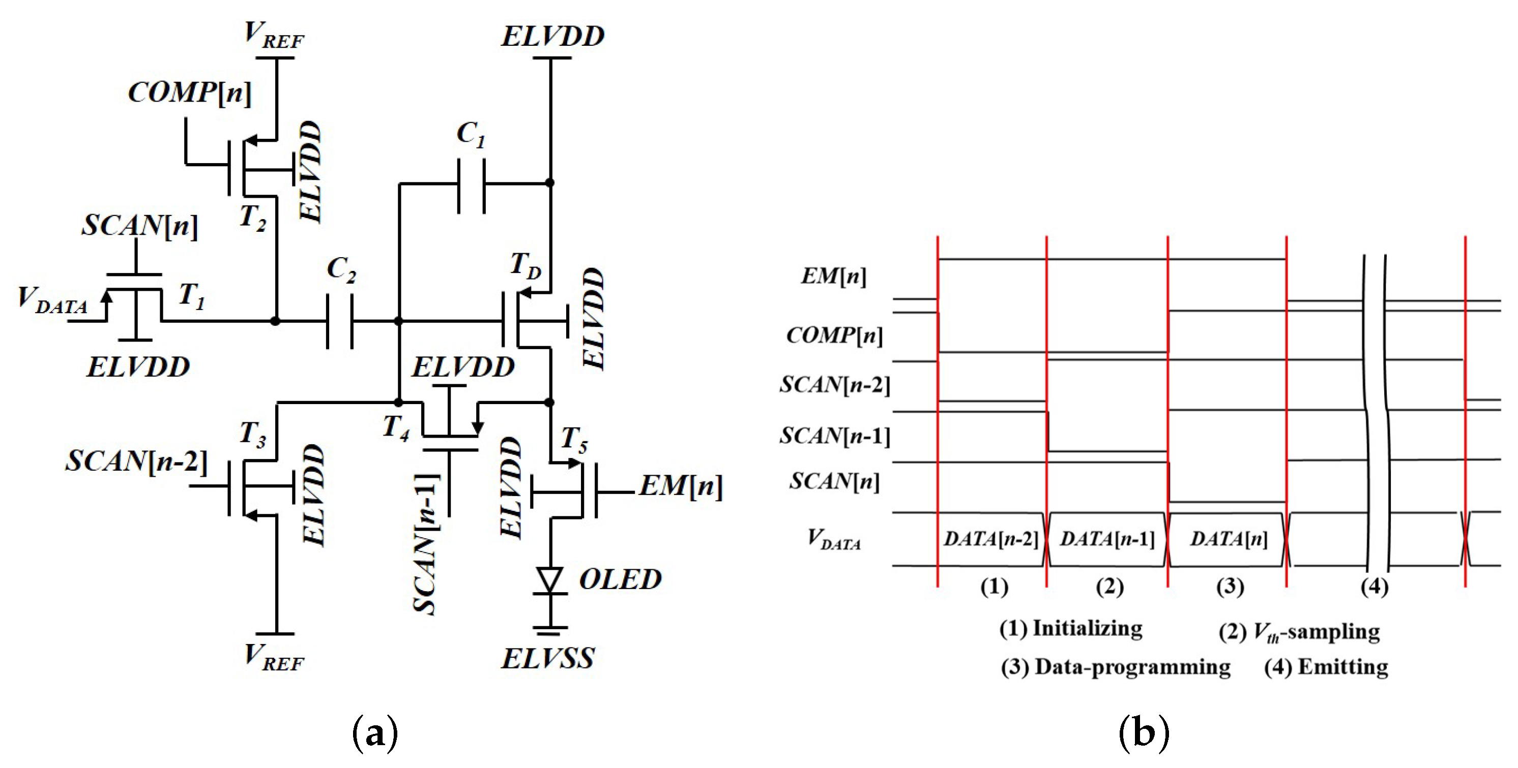
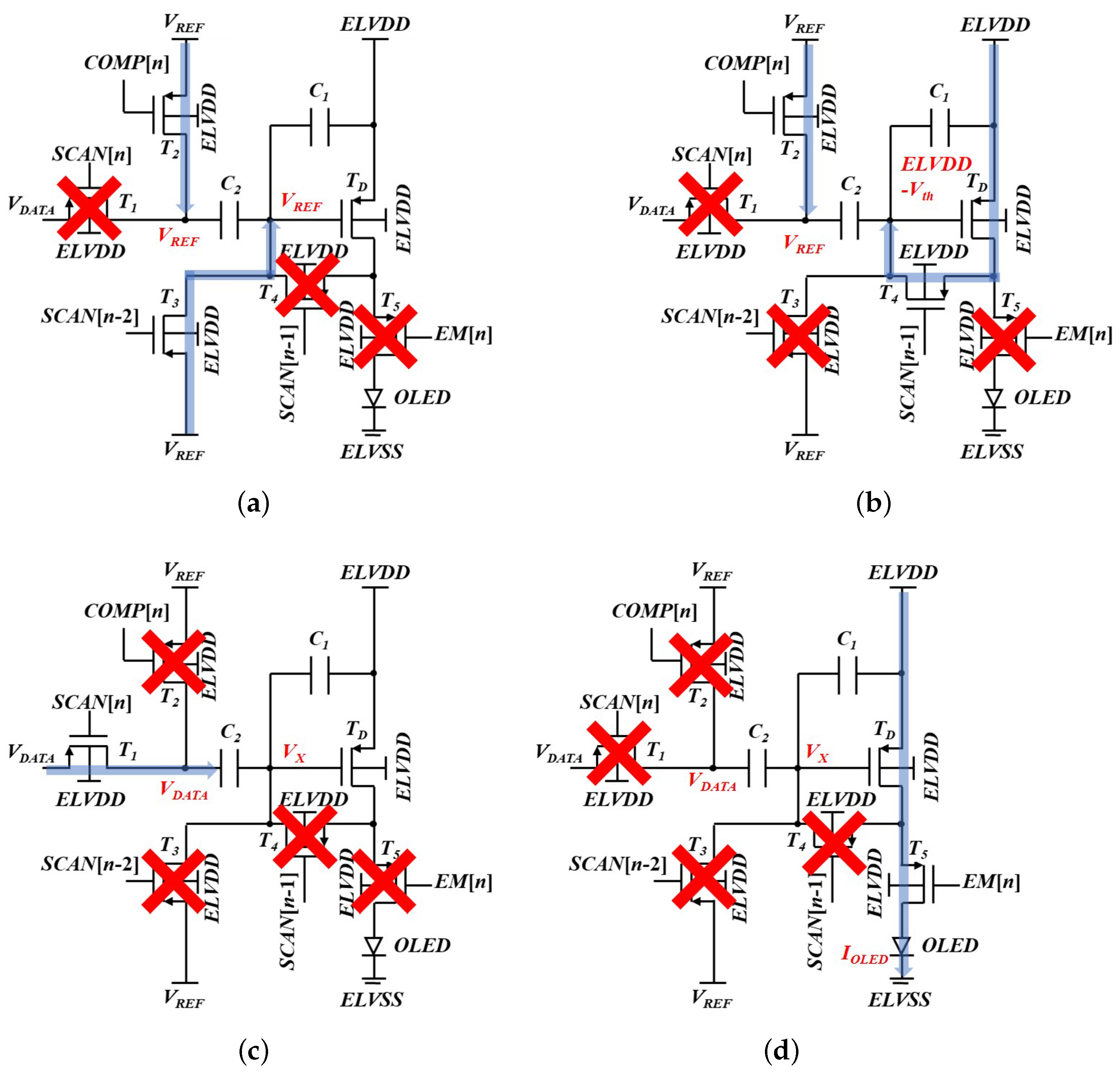
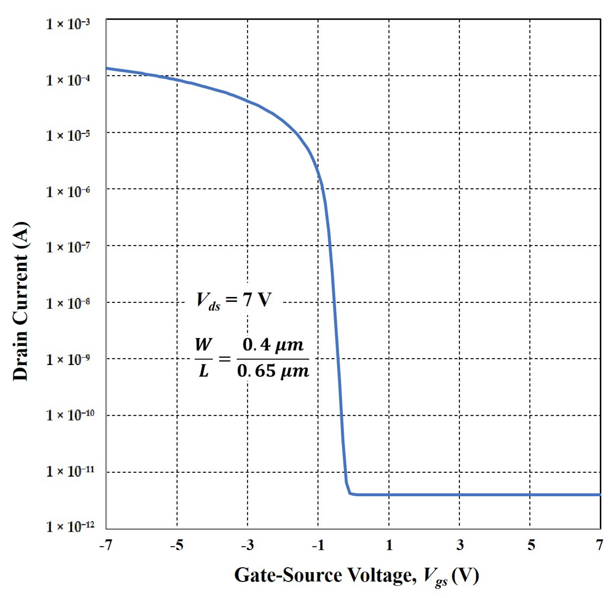
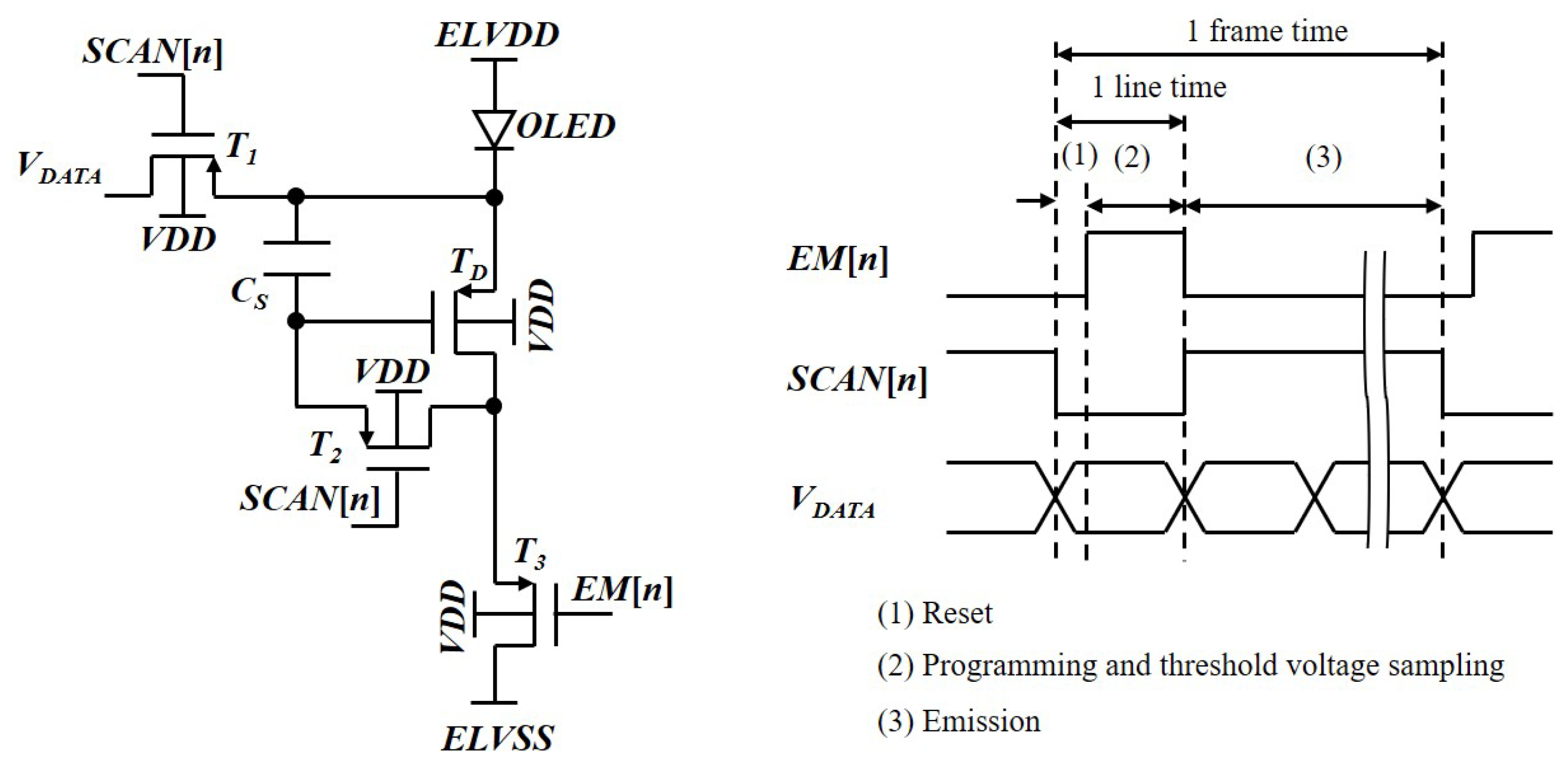
2. Proposed OLEDoS Pixel Circuit
The proposed OLEDoS pixel circuit consists of six PMOS transistors (, , , , , ) and two MIM capacitors (, ) as shown in Figure 1a. Because the lower mobility transistors need a larger gate voltage range for a given current range, PMOS transistors are used in the proposed circuit. While is a driving transistor which adjusts the current through an OLED, other transistors are used as switching transistors. There are five control signals of two previous scanning pulses (, ), a current scanning pulse (), and two additional ones (, ) with one reference voltage (). The timing diagram for the pixel programming is presented in Figure 1b. and are the highest and lowest supply voltages. All bodies of PMOS transistors are connected to , enabling the integration in the same N-well for a small pixel area. In addition, because source and body terminals of are tied to , the proposed pixel circuit is free from the body effect that changes . is given in between and to initialize the gate voltage of via and and to adjust the region of the data voltage () driven by the source drivers via and . enables the diode connection on for compensation, and controls the connection between the drain of and the anode of the OLED. Finally, and are employed to expand the range of up to a supportable one by the conventional DACs of the source drivers.
Figure 1.
Proposed OLEDoS pixel circuit. (a) Schematic. (b) Timing diagram.
The overall operation of the proposed circuit can be explained by four phases, such as initializing, -sampling, data programming, and emitting. To secure enough time for each phase, the whole line time is allocated by using three scanning pulses as control signals.
In the initializing phase of Figure 2a, and turn and , while the other switching transistors stay in the off state. Therefore, the gate voltage of and the terminals of are charged to . This turns on as well because is given to be lower than .
Figure 2.
Operation phases of the proposed pixel circuit. (a) Initializing. (b) -sampling. (c) Data programming. (d) Emitting.
In the -sampling phase of Figure 2b, while , , and are turned off, and are turned on to hold the voltage of on one terminal of and to set the diode connection on . Consequently, the gate voltage of becomes , and the voltages across and change to and . While TFTs show different threshold voltages according to operation regions, CMOS transistors have a common threshold voltage. Therefore, the sampled at the saturation region can be used to compensate for the variation at the sub-threshold region. The total amount of charges on and () is described at the gate node of similar to Equation (1).
In the data programming phase of Figure 2c, only is turned on to charge with . Because the gate node of becomes a floating node without any current paths from itself, the amount of charges () should be equal to as shown in Equation (2), where is the gate voltage of . As a result, is decided by the difference of and multiplied with the ratio of and as presented in Equation (3).
In the final emitting phase of Figure 2d, enables the programmed current to flow through the OLED as described in Equation (4), where operates at the sub-threshold region in the exponential relationship between the drain current and the gate-source voltage. is the thermal voltage, n is a sub-threshold slope factor between 1 and 1.5, and is a sub-threshold current. The resultant current () is independent of the variations on and . In addition, the voltage region of is adjusted by to support the given range of . Because the is scaled by the ratio of , the smaller ratio leads to the larger range over the required range. Furthermore, since source and body nodes of are maintained at for -sampling and emitting phases, the variation can be successfully addressed.
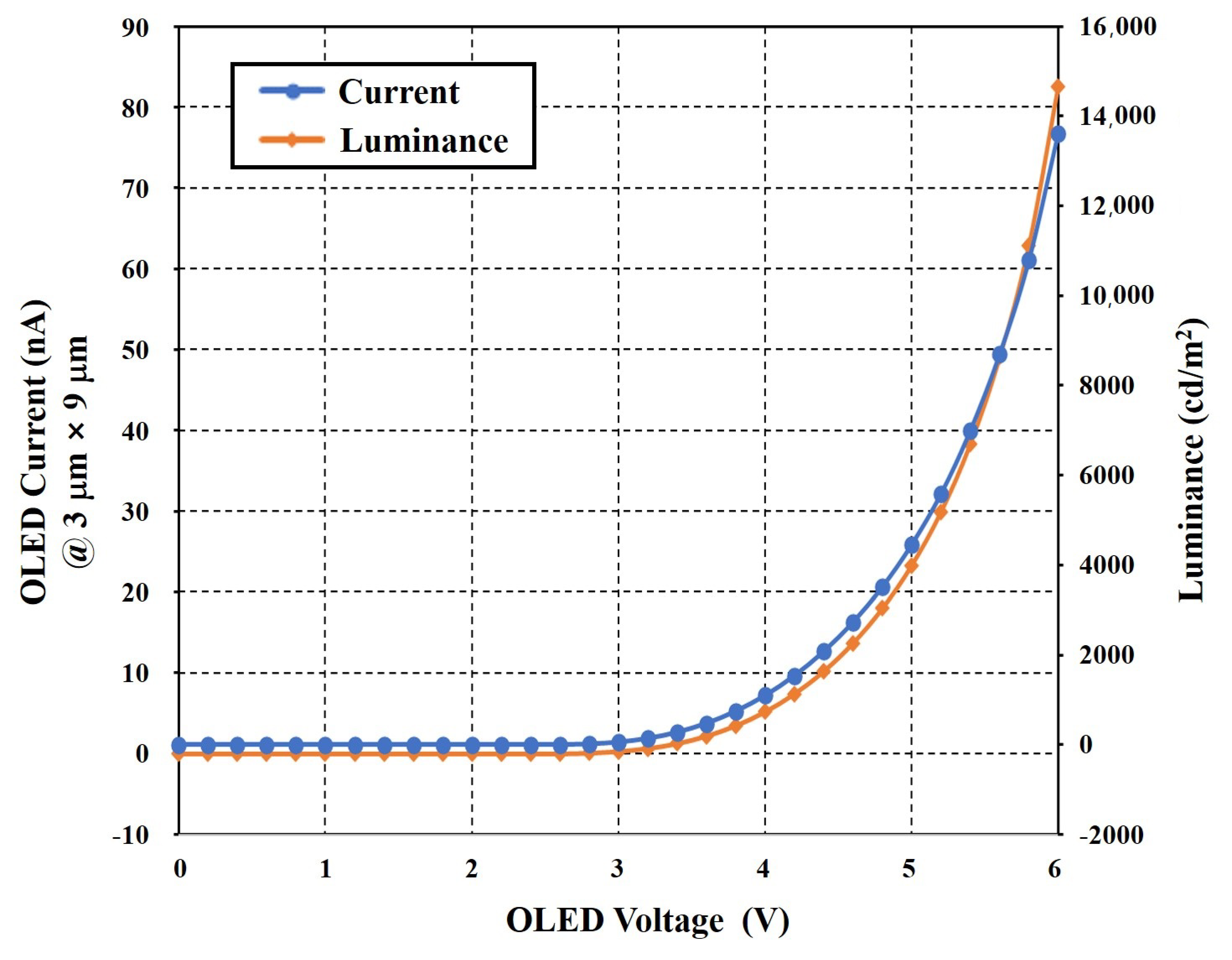
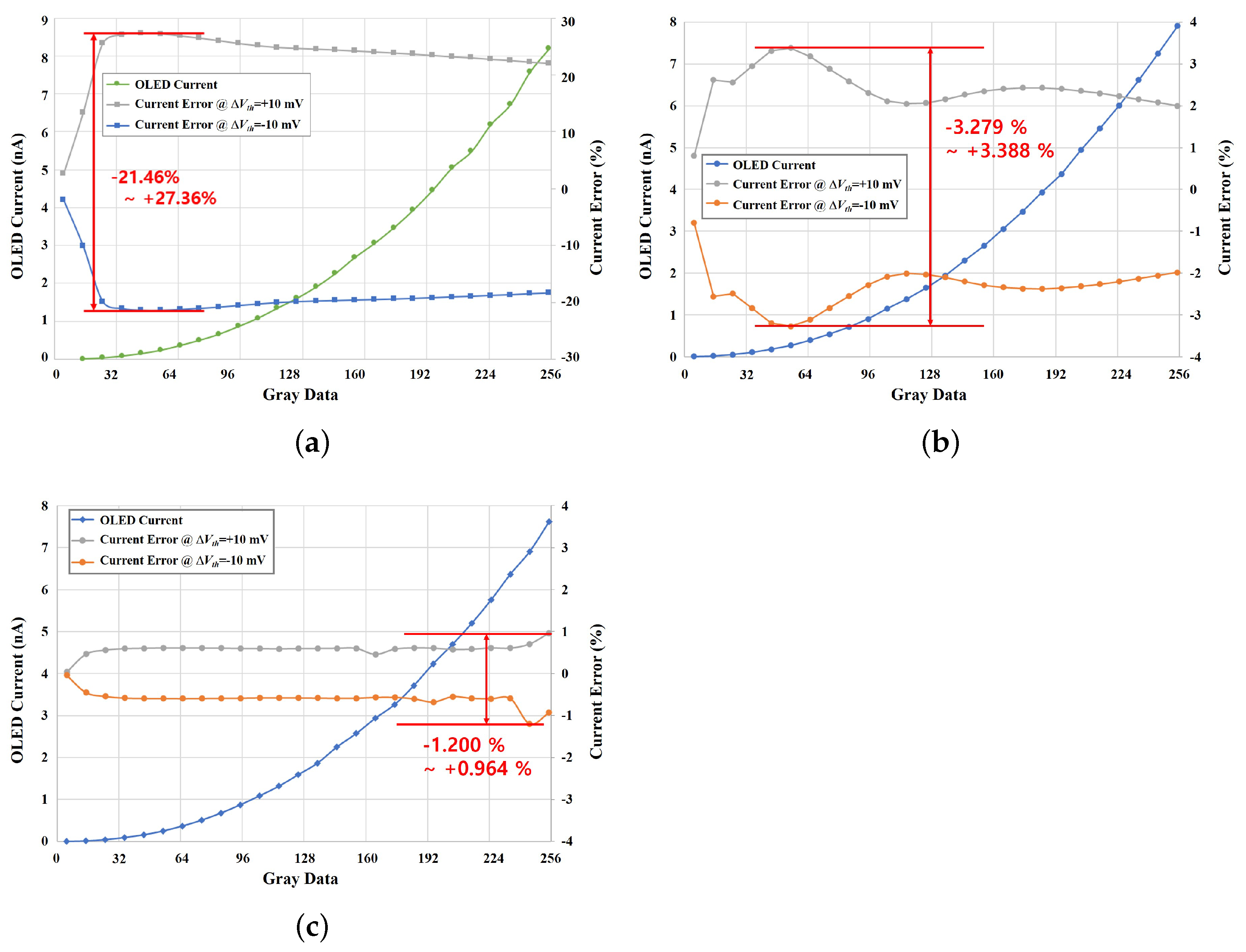
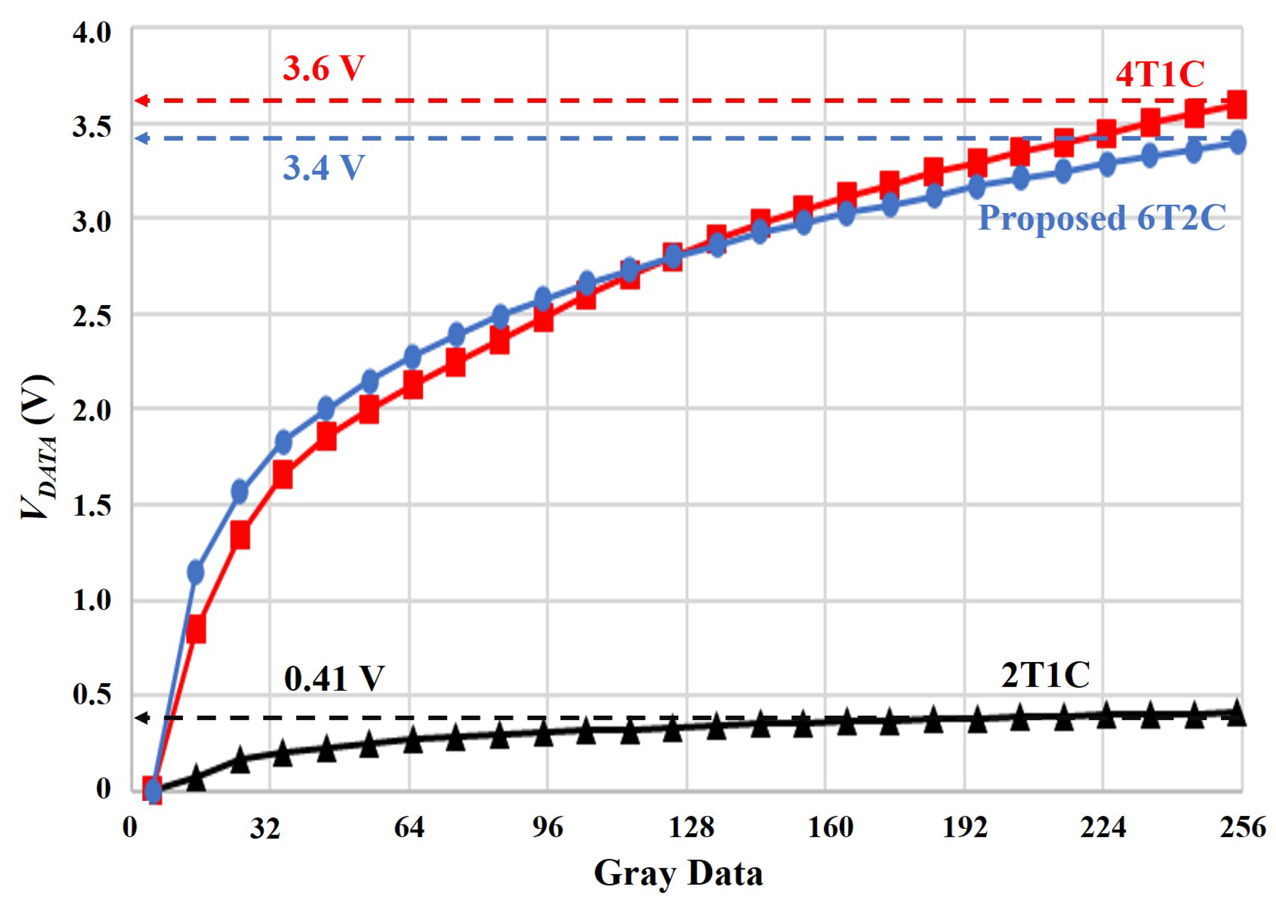
3. Simulation Results
, , and n of PMOS transistors are −0.7688 V, A, and 1.42 at a 110 nm high voltage CMOS process technology. The channel lengths and widths of to and are assigned to the minimum values of 0.65 m and 0.4 m, respectively. The transfer curve of a PMOS transistor is presented in Figure 3. and are 26 fF and 4 fF. While and are set to 7 V and 0 V, is assigned to 4 V. The pixel circuit simulation is conducted over an FHD (1920 × 1080) display at a 60 Hz frame rate by the simulation program with integrated circuit emphasis (SPICE). The maximum is assumed to be around 8 nA to support a luminance of up to 2000 in a blue OLED presented in Figure 4, where the sub-pixel area is assumed to be 3 m × 9 m. These simulation parameters and target display specifications are summarized in Table 1.
Figure 3.
Transfer curve of a PMOS transistor used in the simulation.
Figure 4.
Current and luminance plots of a blue OLED at the sub-pixel area of 3 m × 9 m.
Table 1.
Simulation parameters.
The proposed pixel circuit is compared with a basic pixel circuit of a switching transistor, a driving transistor, and a capacitor (2T1C) as well as the latest CD circuit of three switching transistors, one driving transistor, and one capacitor (4T1C) [21]. Because the previous 4T1C circuit was implemented by NMOS transistors, we have modified it into a PMOS version with of 30 fF to compare the performance as shown in Figure 5, where ELVDD and ELVSS are 7 V and 0 V. In addition, one more supply voltage (VDD) of 4 V is connected to body terminals of all PMOS transistors in the 4T1C circuit similar to its NMOS transistor version, in which all body terminals of transistors are connected to the ground of the voltage higher than the lowest negative supply voltage. of all transistors is fixed at 0.4 m/0.65 m. While the proposed pixel circuit assigns the separate full line times to initializing, sampling, and programming, the 4T1C scheme should finish them within a line time. Therefore, the proposed 6T1C can secure enough charging time for each operation step. However, more transistors in the proposed one lead to a larger circuit area than the 4T1C circuit. The simulation has been conducted at a condition in which the maximum is around 8 nA, and the gamma of a display is 2.2. The differences between and its maximum are depicted in Figure 6 for three pixel circuits. The ranges of the proposed and latest ones are substantially extended to 3.4 V and 3.6 V, compared to 0.41 V of 2T1C.
Figure 5.
PMOS transistor version of 4T1C pixel circuit and timing diagram.
Figure 6.
Extended ranges of 6T2C and 4T1C circuits, compared to the narrow one of the 2T1C circuit.
In addition to the extended range, the compensation performances over the variation () of ±10 mV are evaluated for 2T1C, 4T1C, and the proposed 6T2C circuits. While the 2T1C circuit shows large current errors between −21.46% and 27.36%, as illustrated in Figure 7a, the 4T1C circuit achieves reduced errors between −3.279% and 3.388%, as shown in Figure 7b. Furthermore, the proposed 6T2C pixel circuit reduces the errors into a much smaller range between −1.200% and 0.964%, as presented in Figure 7c. Table 2 compares the performances of previous OLEDoS pixel circuits along with the proposed one. By sacrificing the pixel circuit area due to the large number of transistors, the proposed circuit shows a small current error as well as a wide range without the body effect, along with the assignment of the full line time to all initializing, sampling, and programming.
Figure 7.
OLED currents and current errors over gray data. (a) 2T1C circuit. (b) 4T1C circuit. (c) Proposed 6T2C circuit.
Table 2.
Performance summary and comparison. All pixel circuits have been designed with PMOS transistors of 0.4 m/0.65 m and re-simulated with the same SPICE model parameters.
4. Conclusions
We demonstrate a body-effect-free OLEDoS pixel circuit for high resolution HMDs that compensates for variations and extends the range. The range is adjusted by the ratio of two MIM capacitors, and , and the separate is applied to control the region. The proposed 6T2C circuit achieves a smaller current error range from −1.200% to 0.964% at the variations of ±10 mV in comparison to the range from −21.46% to 27.36% of the basic 2T1C circuit. Furthermore, the proposed body-effect-free structure outperforms the latest 4T1C circuit of the current error range from −3.279% to 3.388%. The range is also enlarged to 3.4 V, which is similar to 3.6 V of the 4T1C circuit, compared to 0.41 V of the basic 2T1C circuit. Consequently, the proposed OLEDoS pixel circuit can contribute to realizing high resolution HMDs for immersive and high quality AR/VR applications sooner.
Author Contributions
Conceptualization, H.N. and J.B.; formal analysis, H.N. and J.B.; resources, H.N. and J.B.; writing—original draft preparation, J.B.; writing—review and editing, H.N.; visualization, H.N. and J.B.; supervision, H.N.; project administration, H.N.; funding acquisition, H.N. All authors have read and agreed to the published version of the manuscript.
Funding
This research was supported by IDEC (EDA Tool) and the Brain Korea 21 Four Program in 2021.
Institutional Review Board Statement
Not applicable.
Informed Consent Statement
Not applicable.
Data Availability Statement
Data sharing not applicable.
Conflicts of Interest
The authors declare no conflict of interest.
References
- Paavilainen, J.; Korhonen, H.; Alha, K.; Stenros, J.; Koskinen, E.; Mayra, F. The Pokémon GO Experience: A Location-Based Augmented Reality Mobile Game Goes Mainstream. Proc. CHI 2017, 2017, 2493–2498. [Google Scholar]
- Al-Azawi, R.; Shakkah, M.S. Embedding augmented and virtual reality in educational learning method: Present and future. In Proceedings of the ICICS 2018, Lille, France, 29–31 October 2018; pp. 218–222. [Google Scholar]
- Farshid, M.; Paschen, J.; Eriksson, T.; Kietzmann, J. Go boldly!: Explore augmented reality (AR), virtual reality (VR), and mixed reality (MR) for business. Bus. Horiz. 2018, 61, 657–663. [Google Scholar] [CrossRef]
- Lungu, A.J.; Swinkels, W.; Claesen, L.; Tu, P.; Egger, J.; Chen, X. A review on the applications of virtual reality, augmented reality and mixed reality in surgical simulation: An extension to different kinds of surgery. Expert Rev. Med. Devices 2020, in press. [Google Scholar] [CrossRef]
- Izard, S.G.; Méndez, J.A.J.; Palomera, P.R.; García-Peñalvo, F.J. Applications of Virtual and Augmented Reality in Biomedical Imaging. J. Med. Syst. 2019, 43, 102. [Google Scholar] [CrossRef] [PubMed]
- Yung, R.; Khoo-Lattimore, C. New realities: A systematic literature review on virtual reality and augmented reality in tourism research. Curr. Issues Tour. 2019, 22, 2056–2081. [Google Scholar] [CrossRef]
- Muñoz-Saavedra, L.; Miró-Amarante, L.; Domínguez-Morales, M. Augmented and Virtual Reality Evolution and Future Tendency. Appl. Sci. 2020, 10, 322. [Google Scholar] [CrossRef] [Green Version]
- Zhan, T.; Yin, K.; Xiong, J.; He, Z.; Wu, S.T. Augmented Reality and Virtual Reality Displays: Perspectives and Challenges. iScience 2020, 23, 101397. [Google Scholar] [CrossRef] [PubMed]
- Han, M.K. AM backplane for AMOLED. In Proceedings of the ASID, New Delhi, India, 8–12 October 2006; pp. 53–58. [Google Scholar]
- Lee, J.H.; Nam, W.J.; Kim, B.K.; Choi, H.S.; Ha, Y.M.; Han, M.K. A New Poly-Si TFT Current-Mirror Pixel for Active Matrix Organic Light Emitting Diode. IEEE Electron. Device Lett. 2006, 27, 830–833. [Google Scholar] [CrossRef]
- Kim, Y.W.; Kwak, W.K.; Lee, J.Y.; Choi, W.S.; Lee, K.Y.; Kim, S.C.; Yoo, E.J. 40 Inch FHD AM-OLED Display with IR Drop Compensation Pixel Circuit. In Proceedings of the SID, San Antonio, TX, USA, 1–5 June 2009; pp. 85–87. [Google Scholar]
- Lee, B.W.; Ji, I.H.; Han, S.M.; Sung, S.D.; Shin, K.S.; Lee, J.D.; Kim, B.H.; Berkeley, B.H.; Kim, S.S. Novel Simultaneous Emission Driving Scheme for Crosstalk-free 3D AMOLED TV. In Proceedings of the SID, Seattle, WA, USA, 25–27 May 2010; pp. 758–761. [Google Scholar]
- In, H.J.; Kwon, O.K. A Simple Pixel Structure Using Polycrystalline-Silicon Thin-Film Transistors for High-Resolution Active-Matrix Organic Light-Emitting Diode Displays. IEEE Electron. Device Lett. 2012, 33, 1018–1020. [Google Scholar] [CrossRef]
- Song, E.; Nam, H. Novel voltage programming n-channel TFT pixel circuit for low power and high performance AMOLED displays. Displays 2014, 35, 118–125. [Google Scholar] [CrossRef]
- Seol, K.H.; Kim, Y.I.; Park, S.; Nam, H. Simultaneous Emission AC-OLED Pixel Circuit for Extended Lifetime of OLED Display. IEEE J. Electron. Devices Soc. 2018, 6, 835–840. [Google Scholar] [CrossRef]
- Kim, H.; Kwak, B.C.; Lim, H.S.; Kwon, O.K. Pixel Circuit for Organic Light-Emitting Diode-on Silicon Microdisplays Using the Source Follower Structure. Jpn. J. Appl. Phys. 2010, 49, 03CD05. [Google Scholar] [CrossRef]
- Kwak, B.C.; Lim, H.S.; Kwon, O.K. Organic Light-Emitting Diode-on-Silicon Pixel Circuit Using the Source Follower Structure with Active Load for Microdisplays. Jpn. J. Appl. Phys. 2011, 50, 03CC05. [Google Scholar] [CrossRef]
- Liu, B.; Ding, D.; Zhou, T.; Zhang, M. A Novel Pixel Circuit Providing Expanded Input Voltage Range for OLEDoS Microdisplays. In Proceedings of the SID, Los Angeles, CA, USA, 23–26 May 2017; pp. 1438–1441. [Google Scholar]
- Hong, S.W.; Kwak, B.C.; Na, J.S.; Hong, S.K.; Kwon, O.K. Simple pixel circuits for high resolution and high image quality organic light emitting diode-on-silicon microdisplays with wide data voltage range. J. Soc. Inf. Disp. 2016, 24, 110–116. [Google Scholar] [CrossRef]
- Huo, X.; Liao, C.; Wu, J.; Yi, S.; Wang, Y.; Jiao, H.; Zhang, M.; Zhang, S. An OLEDoS Pixel Circuit with Extended Data Voltage Range for High Resolution Micro-Displays. In Proceedings of the SID, Los Angeles, CA, USA, 22–25 May 2018; pp. 1373–1376. [Google Scholar]
- Na, J.S.; Hong, S.K.; Kwon, O.K. A 4410-ppi Resolution Pixel Circuit for High Luminance Uniformity of OLEDoS Microdisplays. IEEE J. Electron. Devices Soc. 2019, 7, 1026–1032. [Google Scholar] [CrossRef]
Publisher’s Note: MDPI stays neutral with regard to jurisdictional claims in published maps and institutional affiliations. |
© 2021 by the authors. Licensee MDPI, Basel, Switzerland. This article is an open access article distributed under the terms and conditions of the Creative Commons Attribution (CC BY) license (https://creativecommons.org/licenses/by/4.0/).