Article

A Chopper-Embedded BGR Composite Noise Reduction Circuit for Clock Generator

1
Department of Engineering and System Science, National Tsing Hua University, Hsinchu 300044, Taiwan
2
Institute of Photonics Technologies, Department of Electrical Engineering, National Tsing Hua University, Hsinchu 300044, Taiwan
*
Authors to whom correspondence should be addressed.
Electronics 2021, 10(18), 2257; https://doi.org/10.3390/electronics10182257
Submission received: 29 July 2021 / Revised: 28 August 2021 / Accepted: 31 August 2021 / Published: 14 September 2021
(This article belongs to the Special Issue Design of Mixed Analog/Digital Circuits)

Abstract

:
A chopper-embedded bandgap reference (BGR) scheme is presented using 0.18 μm CMOS technology for low-frequency noise suppression in the clock generator application. As biasing circuitry produces significant flicker noise, along with thermal noise from passive components, the proposed low-noise chopper-stabilized BGR circuit was designed and implemented for a wide range of temperature from −40 to 125 °C, including a startup and self-biasing circuit to reduce critical low-frequency noise from the bias circuitry and op amp input offset voltage. The BGR circuit generated a reference voltage of 1.25 V for a supply voltage range of 2.5–3.3 V. The gain of the implemented BGR operational transconductance amplifier is 84.1 dB. A non-overlapping clock circuit was implemented to reduce the clock skew effect, which is also one of the noise contributors. The noise analysis of a chopped bandgap voltage reference was evaluated through cadence periodic steady-state (PSS) analysis and periodic noise (PNoise) analysis. The low-frequency flicker noise was reduced from 1.5 to 0.4 μV/sqrt(Hz) at 1 KHz, with the proposed chopping scheme in the bandgap. Comparisons of the noise performance of the chopper-embedded BGR, with and without a low-pass filter, were also performed, and the results show a further reduction in the overall noise. A reduction in the flicker noise, from 181.3 to 10.26 mV/sqrt(Hz) at 100 KHz, was observed with the filter. All circuit blocks of the proposed BGR scheme were designed and simulated using the EDA tool HSPICE, and layout generation was carried out by Laker. The BGR architecture layout dimensions are 285.25 μm × 125.38 μm.

1. Introduction

The voltage reference is an integral building block for analog-mixed signal circuits and RF design. A bandgap reference circuit is used to provide a stable reference voltage. At the same time, it also has some internal degradation factors, such as biasing circuitry low-frequency noise, which comprises flicker noise and channel thermal noise; passive components as well as transistor-level noise, are very significant in terms of flicker noise, thermal noise and white noise. The main source of flicker noise is lattice defects at the interface of the silicon and the gate oxide, which creates a dangling bond and energy states. These states randomly trap channel charge carriers, causing a fluctuation in the threshold voltage. The time constant of the capture and release process is a few tenths to several milliseconds. Therefore, the corresponding flicker noise is observed at low frequencies. Another important noise source is the channel thermal noise current, as when it is in saturation, a MOSFET has an inversion layer with limited resistance, and this resistor, similar to any other resistor, generates a thermal noise current [1,2,3,4]. A switched capacitor resistor circuit was implemented in this work to suppress the thermal noise.
An operational transconductance amplifier (OTA) input offset voltage error can be amplified and introduce a significant error in the reference output voltage. These issues need to be addressed to obtain a highly precise and stable reference voltage. A BGR scheme of bipolar junction transistors is more accurate and less sensitive to the process variation, in comparison to all MOSFET ones [5,6,7,8]. In [9], a MOSFET chopper-stabilized BGR scheme was presented. This design reported a significant variation in the reference output due to a maximum of 20% variation in the resistor value during circuit realization. This design approach strongly recommends multiple trimmings, which is a costly procedure. The BGR design in [10] used a Wilson current mirror with BJT for BGR realization. Another method includes curvature minimization to improve the BGR precision by applying circuit techniques. The piecewise linear technique demonstrated better flexibility for curvature minimization [11,12,13,14,15]. It has an additional requirement of overhead circuits, which consume more power to generate nonlinear signals. The proposed architecture strongly emphasizes resistor matching and employs a very effective resistor matching technique in the complete circuit design to obtain highly accurate resistor values and matching. It also includes a startup and a self-biasing circuit with a triggering loop, and an OTA with three chopper configurations for more accurate low-frequency biasing and offset noise suppression. The proposed BGR scheme provides a comprehensive analysis of noise reduction in time, as well as in the frequency domain. A non-overlapping clock was also implemented to obtain a more precise output. A switched capacitor resistor was implemented to achieve a more flexible BGR composite scheme. There are three techniques, namely trimming, correlated double sampling (auto-zero) and chopper modulation, that can be used to suppress low-frequency noise and the op amp offset. Multiple trimming is not a reliable and cost-effective noise reduction process. On the other hand, auto-zero is not a continuous noise reduction method, unlike chopper modulation.
A bandgap reference (BGR) provides a stable dc reference voltage for many analog circuits, such as A/D converters and clock generators using phase-locked loops (PLLs). The proposed BGR architecture and noise suppression biasing scheme can improve the performance of high-frequency noise-sensitive circuits, much like a clock generator/frequency synthesizer. Clock generators are widely used in many communication system applications as an accurate frequency synthesizer. In a clock generator, the VCO output frequency matches/locks with the reference frequency with the minimum Kvco to reduce the jitter noise [16,17,18,19]. At the same time, every block, such as the prescaler, charge pump, loop filter and VCO, creates some amount of noise. The biasing circuit and variation in the power supply also contribute to the noise. Hence, a clock generator requires a low-noise voltage regulator with a high PSRR to suppress supply and unwanted bias circuitry noise [20,21,22,23,24,25].
The proposed BGR circuit block diagram is shown in Figure 1. This architecture describes the chopper-stabilized BGR scheme implementation that suppresses critical flicker noise. It generates a stable voltage reference output for the prescribed process, temperature and supply variation range. Biasing scheme points Vbp1 and Vbp2 in the noise analysis also show a significant reduction in noise by using the proposed BGR circuit. Hence, the proposed architecture is highly effective in reducing the noise of the clock generators. The structure of this manuscript is summarized as follows: Section 2 describes the proposed chopper-stabilized BGR composite architecture; Section 3 explains the key layout features; Section 4 shows the results; and the conclusion is discussed in Section 5.

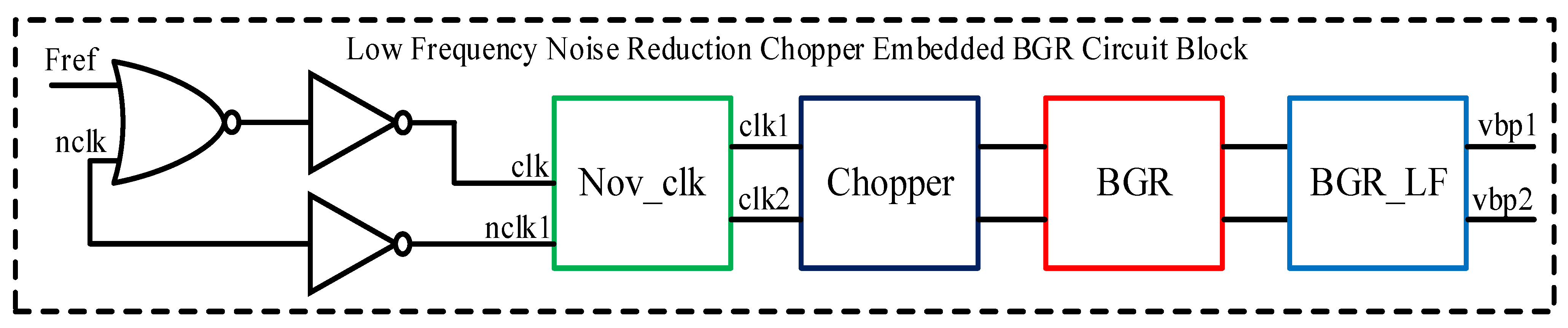
2. Chopper-Stabilized Composite BGR Scheme

To suppress unwanted low-frequency noise and input offset errors, three chopper circuits were implemented in the BGR. One chopper circuit was used at the input pair of the BGR and OTA, and the other two chopper circuits were implemented in the PMOS and NMOS current mirror branches. A non-overlapping clock circuit was also designed to suppress the clock skew effect, which is also one of the noise sources. A detailed OTA schematic of the proposed BGR scheme is shown in Figure 2.

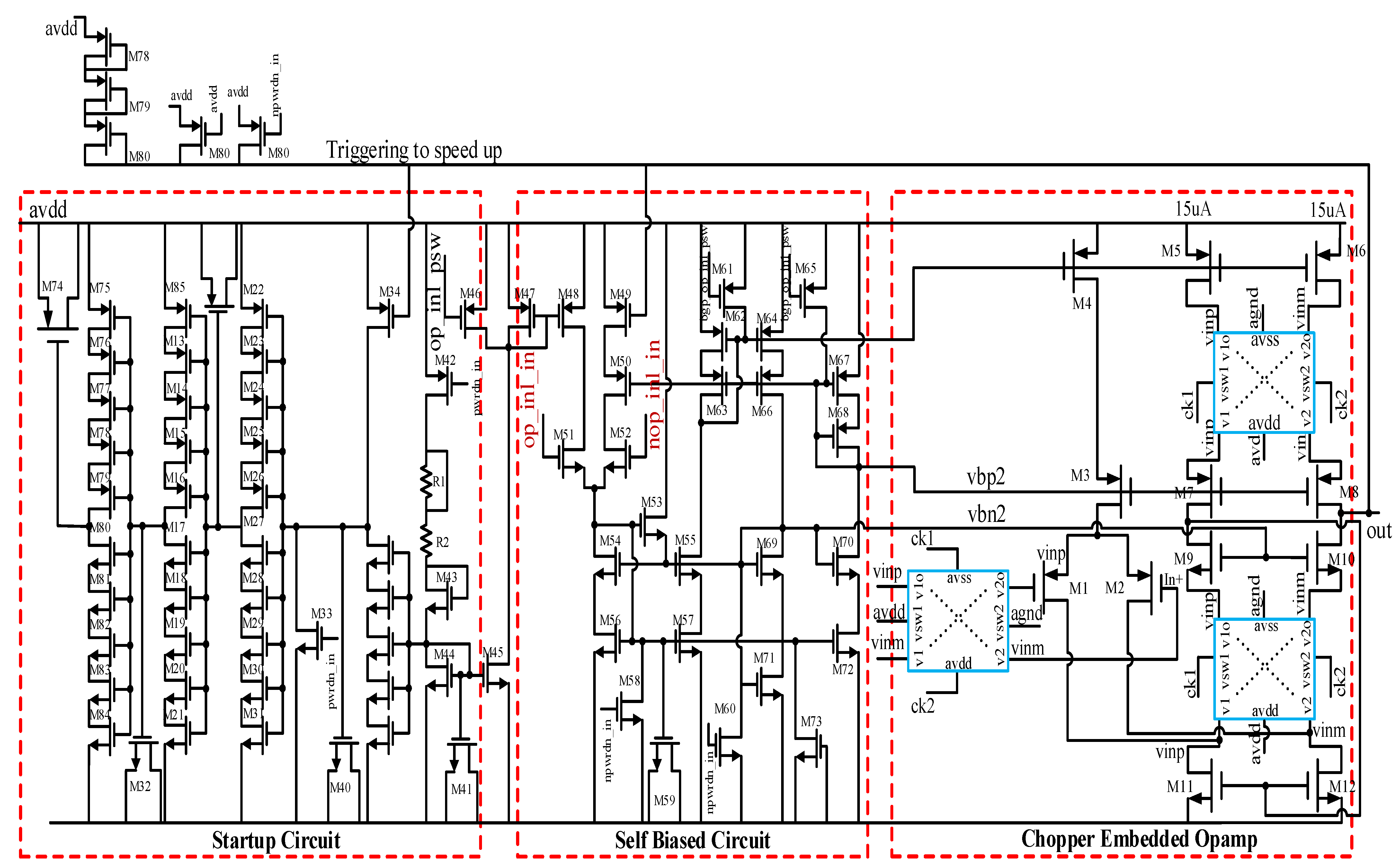
2.1. BGR Chopper-Embedded OTA with Startup and Self-Biasing Circuit

The proposed BGR core comprises self-bias, startup, stop/power-down and a folded cascode op amp with a chopper circuit. The block diagram architecture is displayed in Figure 1, while the core op amp with a chopper schematic is presented in Figure 2.

2.1.1. Operational Transconductance Amplifier

A folded cascode op amp was employed for the OTA to obtain a large common mode range, a high PSSR and output resistance. There are three choppers embedded in the folded cascode structure, as shown in Figure 2. One chopper is in the input pair as a square wave modulator, and the other two are in the PMOS and NMOS cascode branches for demodulation. The OTA structure has a startup/delay circuit and a safety power-down circuit, as discussed below.

2.1.2. Startup Circuit

There may be many degenerate bias points, including the zero current state. This can push the BGR into a non-desired equilibrium state. Hence, to avoid any such possibility, a startup circuit was designed with a large delay (10~200 μs) and supply-independent biasing. This circuit block is shown in Figure 2, where there is an active biased current mirror formed by M44 and M45 and a pull-down resistor. A differential input configuration was introduced to first initialize the startup circuit and then to infuse a large delay with a ramp supply voltage to settle down bias points Vbp2 and Vbn2. This prevents the core circuit from being stuck at any possible degenerate bias level. After the execution of pulse switching at node bgp_op_ini_in in the stipulated time delay duration, bias points Vbp2 and Vbn2 are established, the core op amp circuit starts working with self-bias and the startup circuit is stopped. At the beginning of the circuit operation, there may be a large difference at the differential switching of op_inl_in and nop_inl_in. Hence, a triggering loop circuit was designed from the output to the startup/delay circuit to speed up and wake up the circuit faster through transistors M34 and M49.

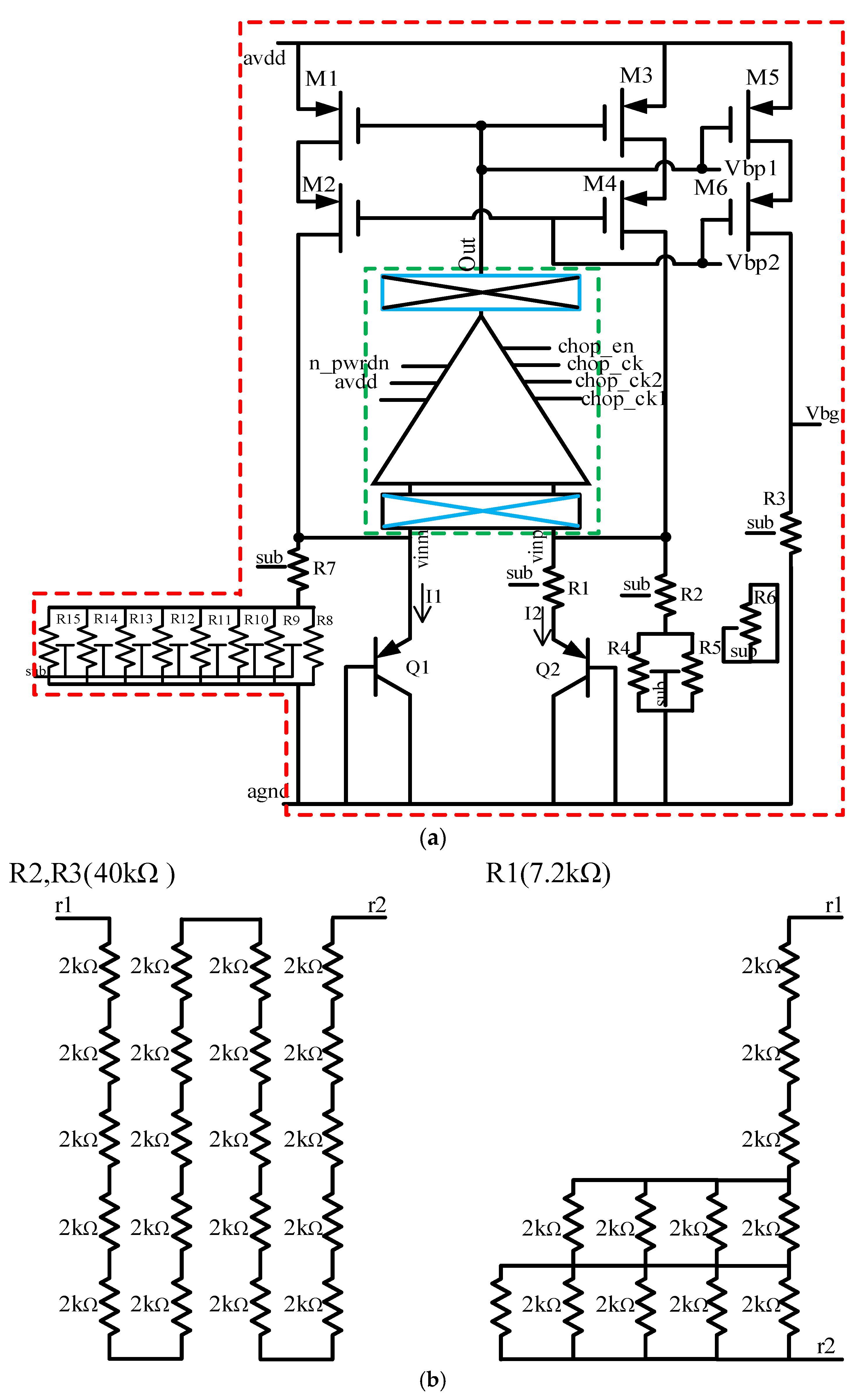
2.2. BGR Operating Principle

The BGR block diagram is shown in Figure 3a. It contains a chopper-embedded OTA, a PMOS cascode current mirror, two bipolar transistors (BJTs) and polysilicon resistors with a low temperature coefficient. PNP BJTs are used and realized by parasitic BJTs using CMOS technology. In the circuit, multiple symmetrical resistors, R8–R15, of 2 kΩ were implemented instead of a single value resistor. In this parallel configuration, the unit resistor value is identical to the resistor R7 of 2 kΩ. For circuit optimization, a resistor value of 250 Ω was obtained using eight identical 2 kΩ resistors in parallel. This reduced variation and improved the accuracy of the resistor value.
Similarly, for other resistor values in the BGR architecture, the emphasis is on the perfect matching of the lowest variations in the post-layout values. The implemented resistors using an identical unit value resistor are shown in Figure 3b. To realize 40 kΩ and 7.2 kΩ value resistors, a symmetrical and equal value resistor of 2 kΩ was applied. This may consume more area, but it improves the required matching criteria in the layout. BJT Q2 was produced eight times in comparison to Q1 by taking n = 8 in the final expression. All component dimensions are shown in Table 1. The PMOS cascode current mirror improves the supply rejection and maintains the branch current and voltage equality in the circuit.
This architecture has the key feature of important components functional flexibility, such as enabling/disabling non-overlapping clocks, and a chopper circuit in the BGR. It also contains an additional safety feature of power-down.
This architecture also realizes reduced noise biasing points Vbp1 and Vbp2 for further clock generator application. Their noise analysis is also discussed in the subsequent sections.
The working principle of the BGR provides the following expression for V b g :
V b g = I M 6 × R 3   [   I M 4 = I M 6   ] I 2 = Δ V B E R 1 = V T   l n ( n ) R 1 V b g = V B E 1 R 7 + (   R 8 R 8 R 12 ) + V T   l n ( n ) R 1 I M 4 = V B E 1 R 2 (   R 4   R 5   ) + V T   l n   ( n ) R 1 V b g = I M 4 × R 3 V b g = R 3 [ V B E 1 R 2 + (   R 4 R 5 ) + V T   l n ( n ) R 1 ]
The proposed architecture generates a stable 1.25 V reference voltage using the device parameters shown in Table 1.
The Monte Carlo simulation graph is shown in Figure 4. This was performed more than one hundred times to test the BGR startup circuit. The simulation graph shows a stabilized bandgap reference output Vbg, biasing voltages Vbp1 and Vbp2, and power-down signal voltage waveforms.

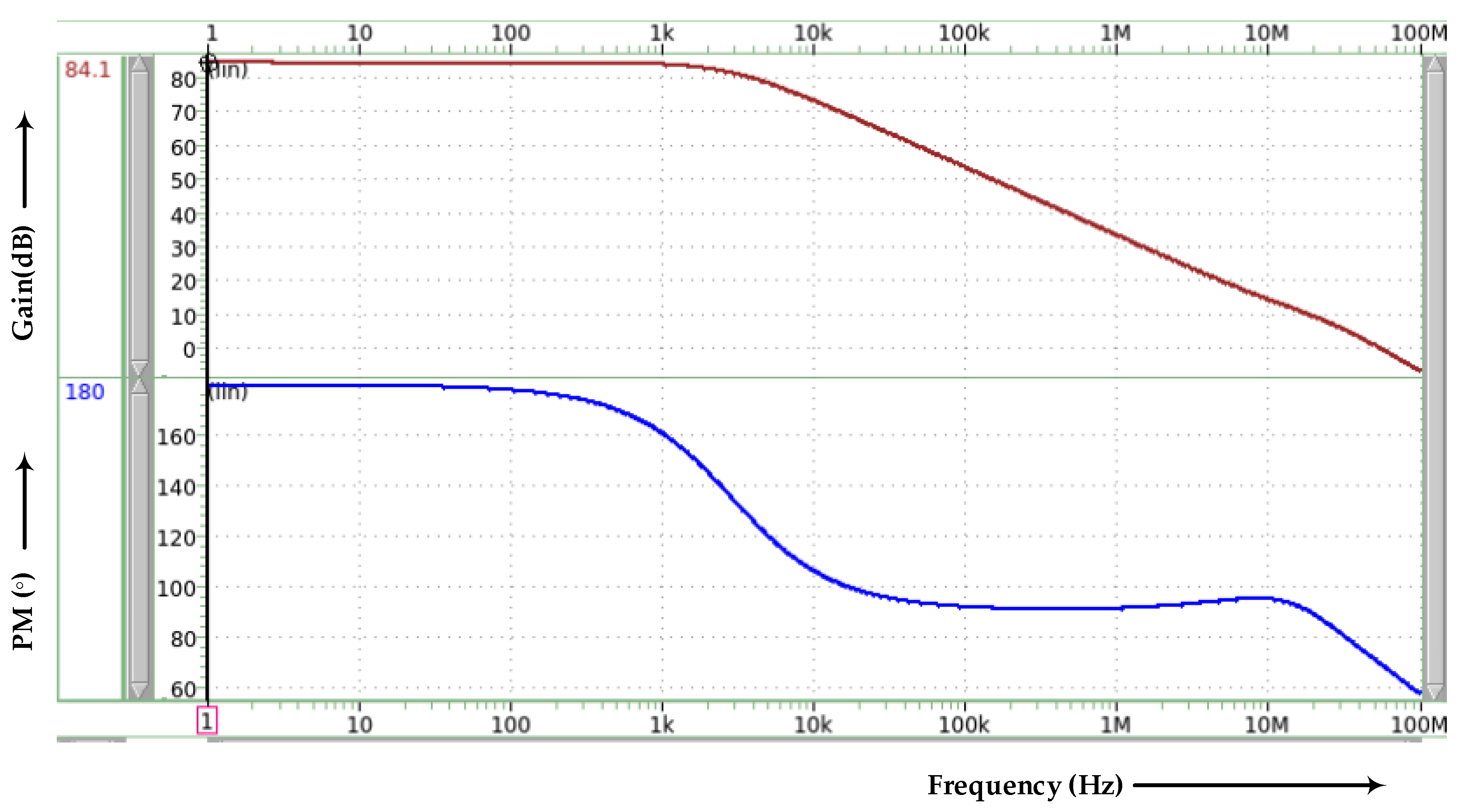
Operational Amplifier Analysis

The BGR operational amplifier gain and phase margin were simulated with 3.3 V ± 10% variation in the supply voltage at 3.3 V, 2.97 V and 3.63 V. The post-simulation OTA gain was 84.1 dB, with a phase margin of 59.48. The simulation graph is displayed in Figure 5.
For more accuracy, the operational amplifier was simulated and tested for all the process corners, voltages and temperature (PVT) variations. The post-simulation results are summarized in Table 2.
The noise analyses of the operational amplifier at different frequencies and for various process corners are summarized in Table 3.

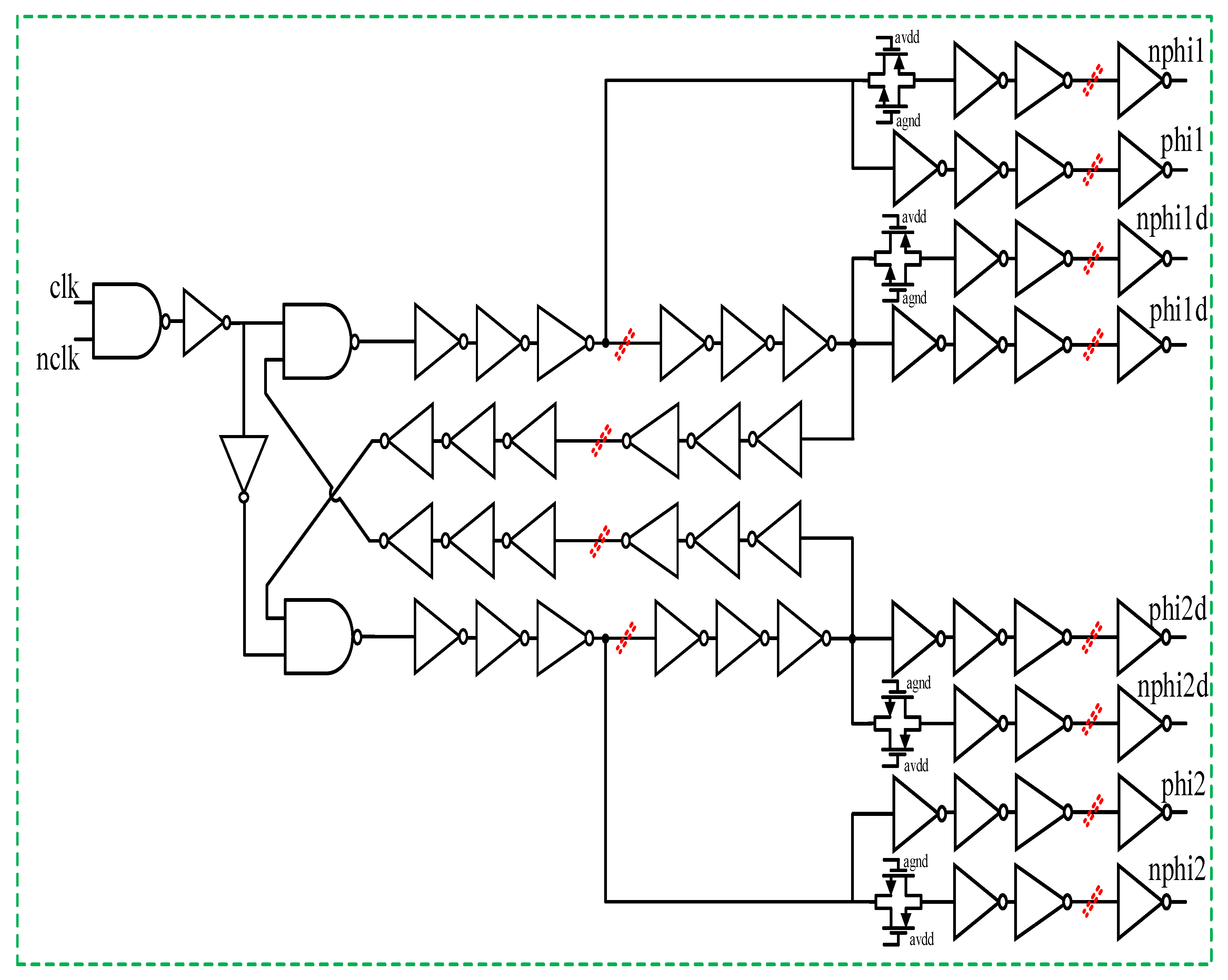
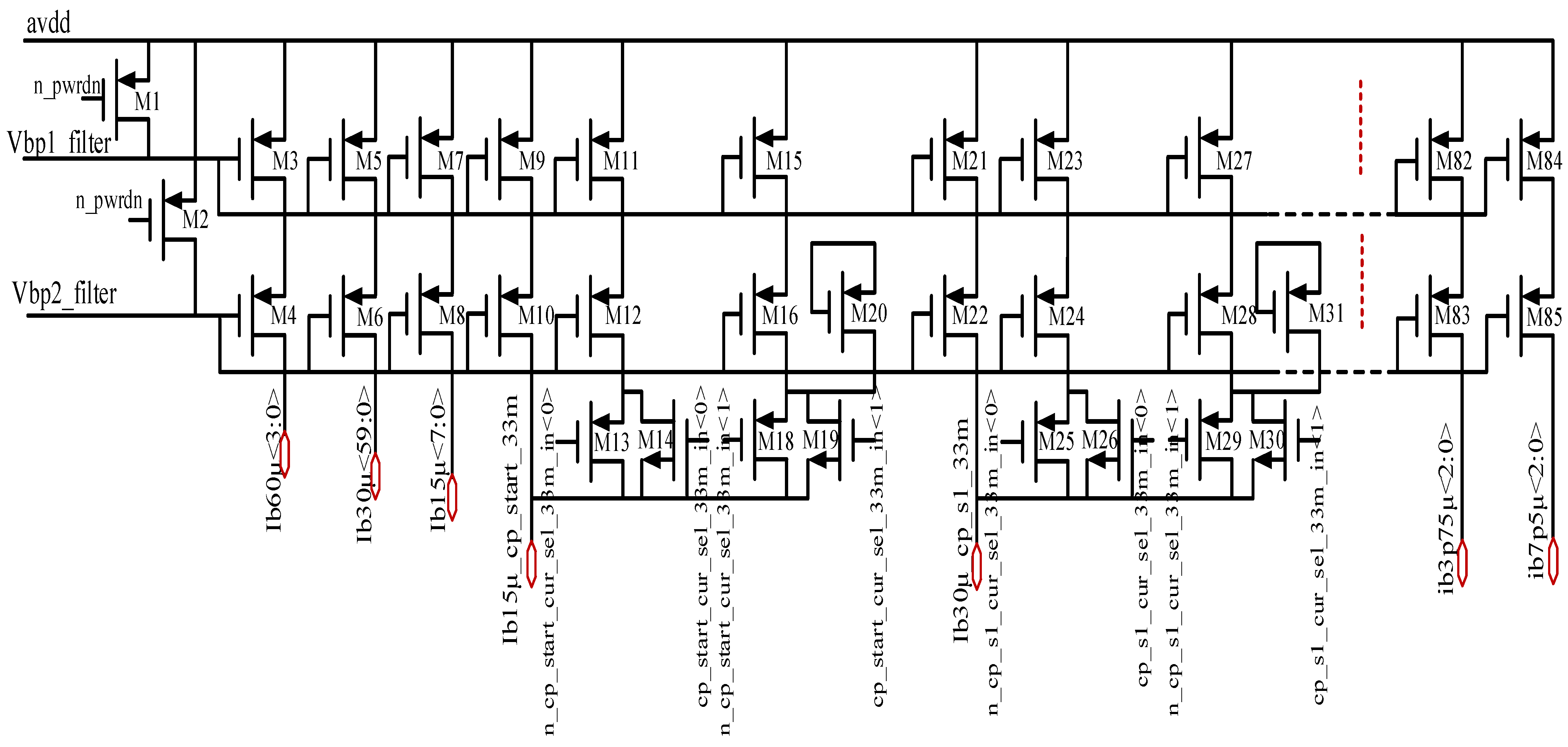
2.3. Non-Overlapping Clock Implementation

Precise clock switching is important for analog and digital systems. The clock signal controls the switching sequences and executes the entire operation of the circuit. Nowadays, a high clock frequency is desirable to improve the system performance, but the non-ideal effects of the increased frequency may result in clock skew and race conditions. To avoid these issues, two-phase non-overlapping clocks were implemented. There is a dead time between the clock edges. The non-overlapping clock signals are executed at the same frequency, and for a short time duration between the pulses; none of them are high. The non-overlapping clock signals are derived from the global overlapping clock signal inside each block to control the skew between the phases of the non-overlapping clock signals. This also reduces the capacitive loading on the global overlapping clock and improves the performance of the timing path. On-chip non-overlapping inverting clocks clk1 and clk2 were implemented from a global off-chip overlapping clock for the chopper circuit, as well as for the switch capacitor resistor realization. Their schematic and simulation graphs are shown in Figure 6 and Figure 7.

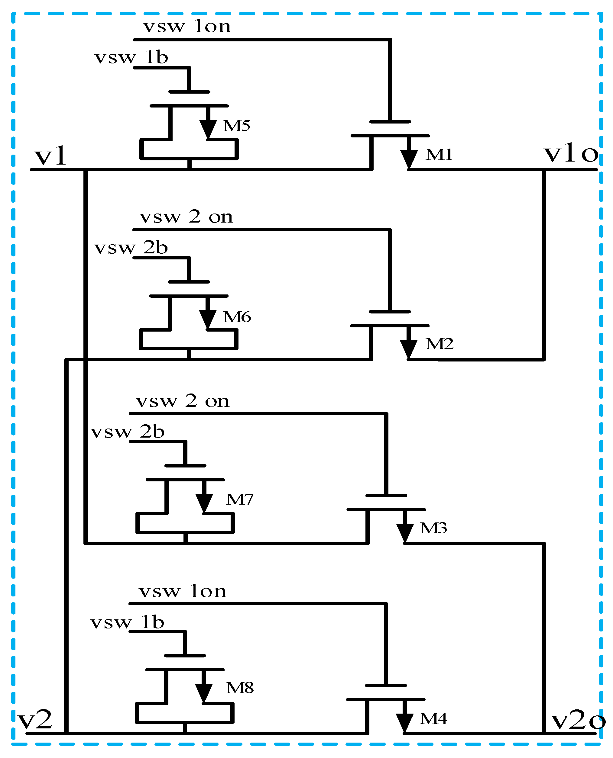
2.4. Chopper Circuit Embedded in the OTA

The core of a BGR, delay circuit, bias circuit and OTA always has some low-frequency 1/f noise, resistor thermal noise and offset noise. These noises may severely degrade the bandgap reference accuracy performance. These unwanted effects can be eliminated/suppressed by the chopper circuit that is implemented in the BGR core circuit, as shown in Figure 2. Its transistor level schematic is shown in Figure 8. The chopper circuit comprises four switches: M1, M2, M3 and M4, which are driven by two phase non-overlapping clock signals: clk1(vsw1on) and clk2(vsw2on). The input modulator comprises M1, M2, M3 and M4, and transposes the input differential signal applied at the terminals vinp and vinm. This reduces the input pair mismatch error by swapping the signals at the vinp and vinm of the op amp. Here, a dummy switch is used with every swapping switch in order to cancel out the channel charge effect. Swapping or reverse polarity switches are able to multiply the analog input signal by +1 or −1. As switches can be realized ideally in the CMOS technology, this chopper circuit thus works as a square wave modulator for chopper-stabilized amplifiers. In Figure 2, the square wave modulator chopper circuit is used at the input of the folded cascode structure, and the second square wave modulator chopper circuit is used at the folding node in the PMOS cascode current branch at the output. After the input differential pair, another significant source of noise is the folded NMOS current mirror branch. Hence, the third chopper circuit is used for higher accuracy. The input signal moves through the first square wave modulator, which turns into a square wave and becomes amplified by the high amplifier gain, and then it is demodulated again to dc at the amplifier output by the second chopper switch. Here, the key point is that the amplifier offset and bias noise are also amplified with the input signal, but they are modulated only once through the amplifier output chopped modulator, meaning that the offset becomes bigger at the output of the amplifier and is filtered out by the low-pass filter. Hence, the input signal is modulated twice and remains unchanged, while the offset is modulated once, passed through the low-pass filter and then filtered out. We implemented a low-pass filter by using the switched capacitor resistor to further suppress the resistive thermal noise. The chopper switches are driven by the complementary non-overlapping clock signals clk1 and clk2 with a 50% duty cycle for the modulated square wave. There is one input chopper, one output PMOS chopper and one extra NMOS current mirror chopper. Here, the extra NMOS chopper cuts the 1/f noise and the offset of the NMOS, thereby providing an additional advantage.
The chopper is fully differential, meaning that it generates matched spikes and therefore a low offset. The chopper-stabilized bandgap reference output was simulated in the time domain as well as in the frequency domain. Figure 9a,b shows the time domain simulation with the removal of noise glitches, when the chopper circuit is enabled. Figure 9a shows the bandgap reference output voltage Vbg with the chopper-disabled output. Here, the chopper circuit is disabled, meaning that Vbg has glitches, while in Figure 9b, the chopper circuit becomes enabled, and therefore, the output Vbg has no glitches.
However, some spikes appear in the chopper-enabled Vbg output. This is due to the clock feedthrough effect of non-overlapping clocks.
The circuit was simulated for all process corners with a 3.3 V ± 10% supply voltage at variations of 3.3 V, 2.97 V and 3.63 V and temperatures of 50 °C, 125 °C and −40 °C for the TT, SS and FF corners. Glitches were reduced effectively in all three corners post-simulation when vchop was enabled, as shown in Figure 9b. The proposed BGR output curvature with an output voltage of 1.25 V for a wide temperature range is shown in Figure 10. The simulated graph has a variation of 800 μV for the TT corner. The PSRR is −66.8 dB for the typical corner.

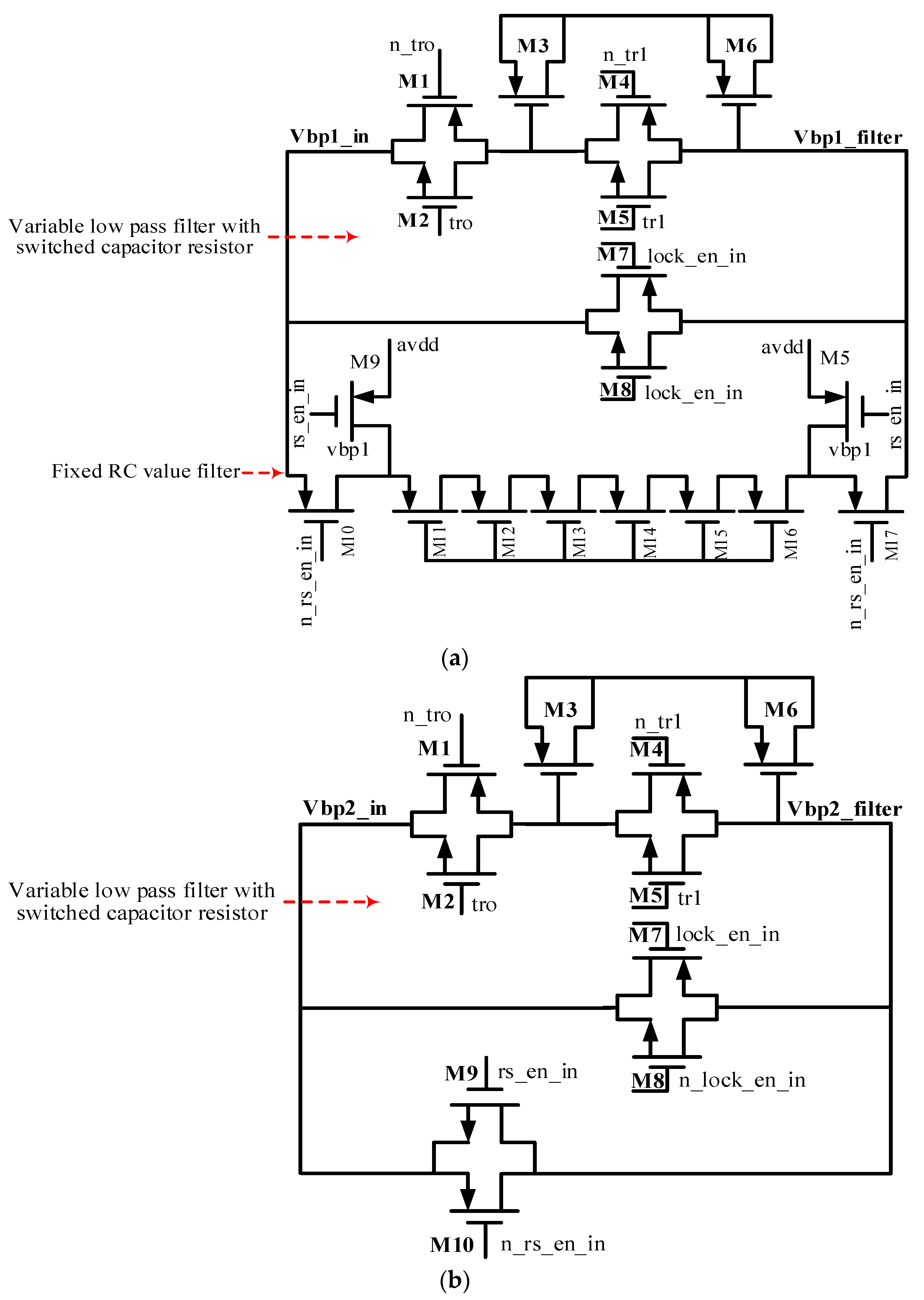
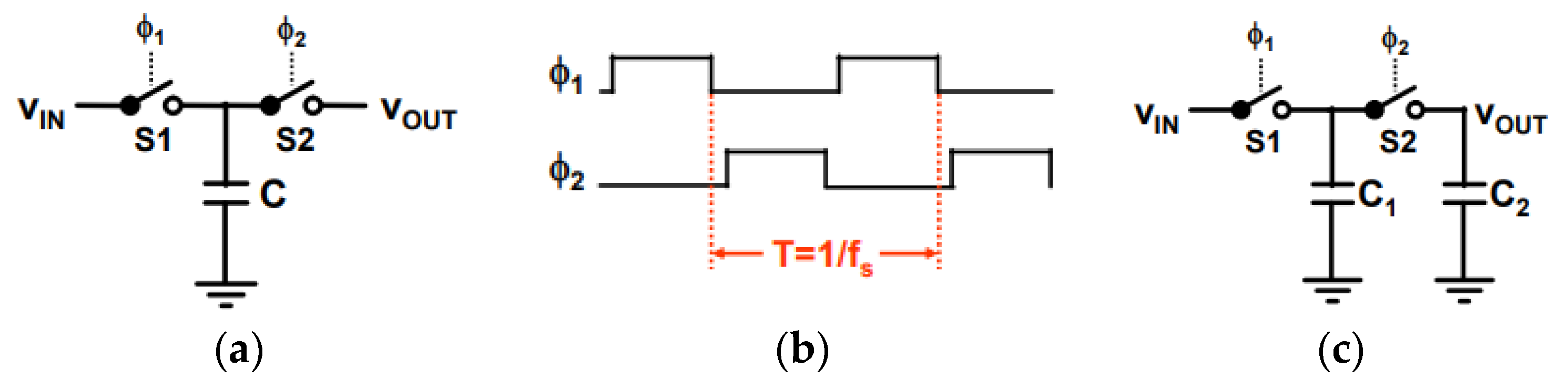
2.5. Switched Capacitor Resistor and Low-Pass Filter

A low-pass filter (LPF) was designed and implemented to filter the high-frequency noise component in the chopper-embedded BGR output. Two low-pass filter circuits, Vbp1_filter and Vbp2_filter, were realized, as shown in Figure 11. Vbp1 has a low-pass filter with a switched capacitor resistor for variable desired resistor values and another fixed RC value filter configuration. It also has a direct pass to the BGR output, without filter application. All these three options provide multiple simulation flexibilities. Another filter, Vbp2_filter, was implemented for the cascode devices. Cascode devices are more immune to noise, hence the use of only one filter configuration.
A switched capacitor resistor is very compact and is suitable for the on-chip fabrication of any desired resistor value. The resistor value depends only on the ratio of the capacitance and the switching frequency. An equivalent switched capacitor resistor is shown in Figure 12a. It has one capacitor, C 1 , and two switches, S1 and S2. A transmission gate is used for the switches S1 and S2, and non-overlapping clock signals are applied, as shown in Figure 12b. The low-pass filter configuration after adding a capacitor, C 2 , at the output of the switched capacitor resistor, as shown in Figure 12c. The filter loop bandwidth is less than 5 KHz for low-frequency noise removal.
With the switching sequences of switch S2 being closed and switch S1 being open, and switch S1 being closed and switch S2 being open, we can transfer a charge q from the input VIN to the output VOUT, with the expression:
q = C   ( V I N V O U T )
The average current flowing from V I N to V O U T is:
I = q/t = qf
Hence:
I = f C   ( V I N V O U T )
Therefore:
R = 1/fC
A 3 dB bandwidth can be expressed by the following expression. Its schematic representation is shown by Figure 12.
ω−3db = 1/ReqC2 = f × C1/C2
f−3db = (1/2Π) × f × C1/C2

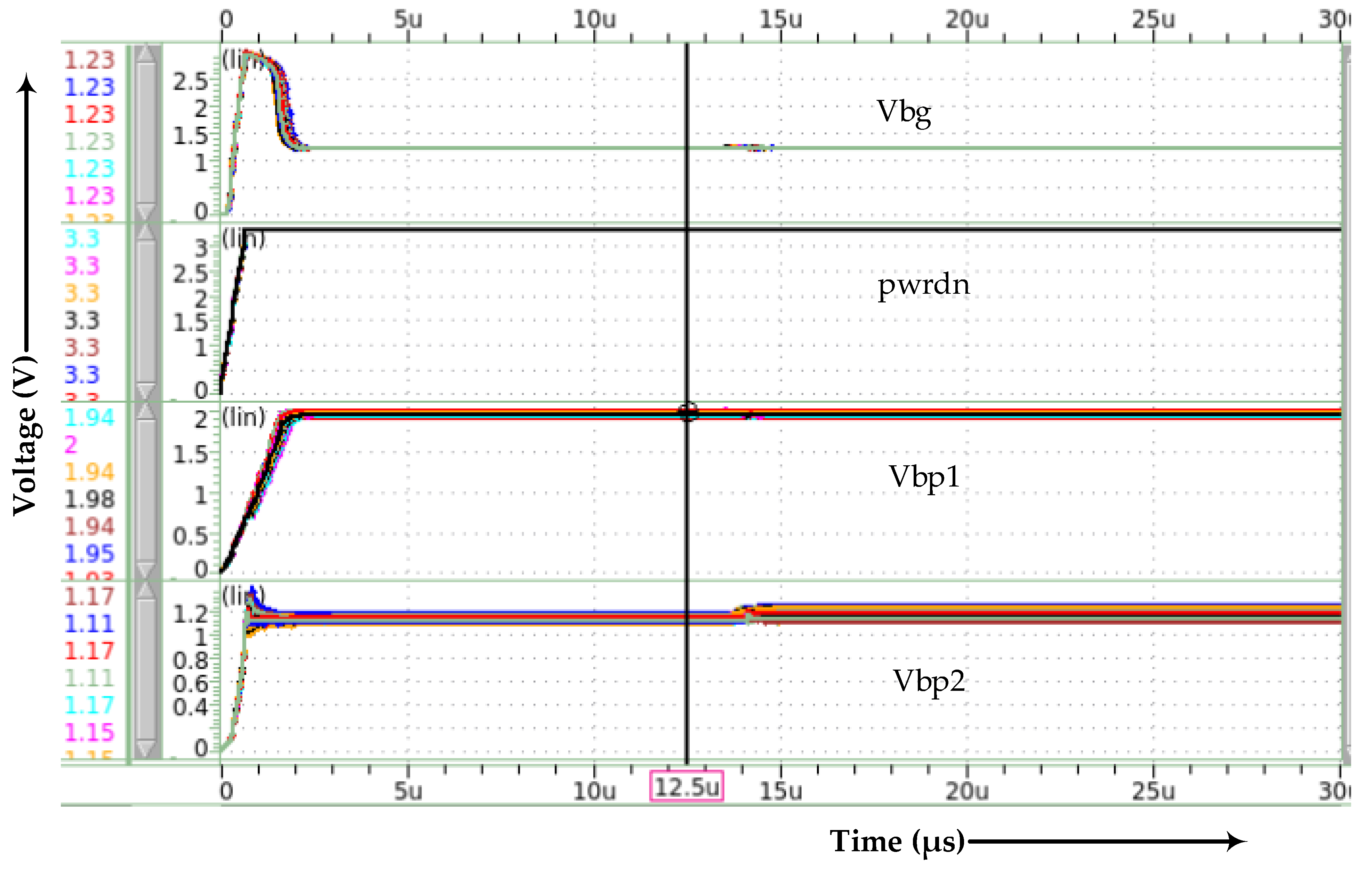
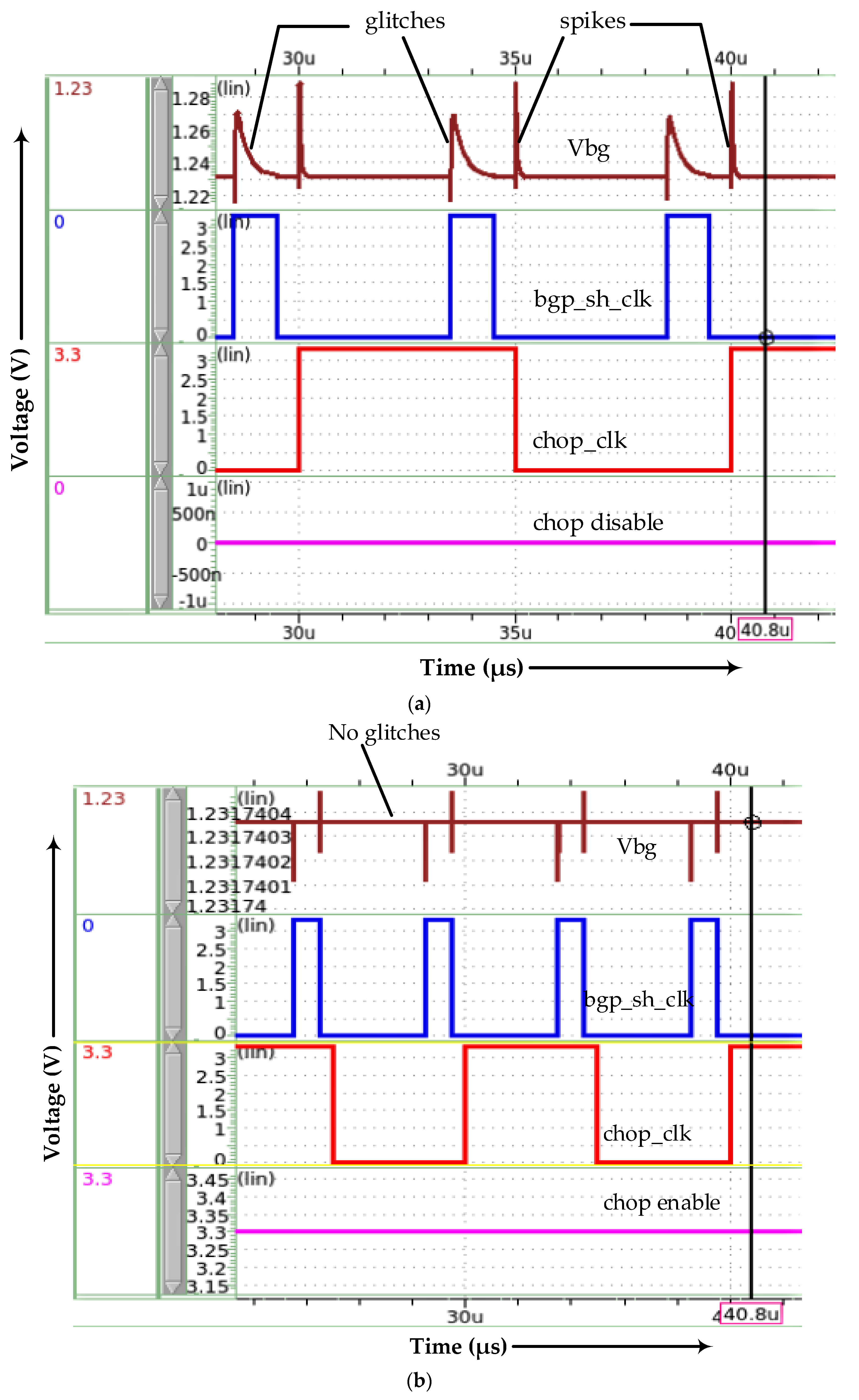
2.6. Chopper-Enabled Bias Pre- and Post-Simulation

For more accuracy, the BGR output voltage and key nodes were also simulated and were observed to check for any possible variations and the performances of the TT, SS and FF corners in the pre- and post-circuit simulations. Table 4 summarizes the pre and post-simulation results and performances. It is observed that the Vbg and key biasing node voltages have significantly less variations in the pre and post-simulations. The lowest post-layout variation is achieved by incorporating the symmetric and matching component strategy discussed above.
The composite BGR circuit was further used to generate a very low noise bias circuit for the clock generator sub-blocks using the Vbp1_filter and Vbp2_filter biasing nodes from the BGR scheme. The schematic diagram of the clock generator bias sub-blocks is shown in Figure 13. A pre and post-simulation was performed to observe the current value at different clock generator bias circuit nodes for the TT, SS and FF corners. The simulation results and performances are summarized in Table 5 and Table 6.

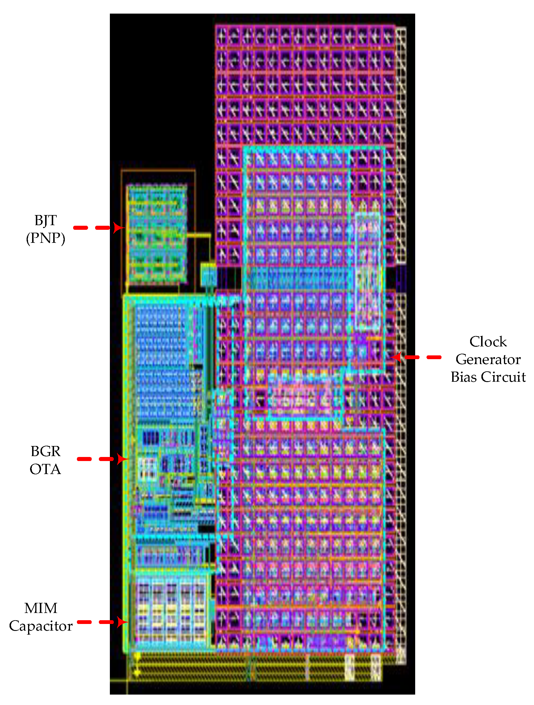
3. Chopper-Embedded BGR Layout

The chopper-embedded BGR circuit layout with all sub-blocks is shown in Figure 14, and the BGR with a bias circuit sub-block layout is shown in Figure 15.
The chip layout was generated through the 0.18 μm CMOS process with dimensions of 285.25 μm × 125.38 μm. For better matching, a resistor layout was also created using a common centroid with dummies. At the same time, each resistor was constructed to be long so that contact resistance becomes very small and does not have an influence. Polysilicon resistors with a low temperature coefficient were used for the resistor layout. This is better material, compared to diffusion resistors, for precise value fabrication.
The performance comparisons of the proposed BGR circuit with other bandgap references are shown in Table 7. This shows the comparisons between this work and other previous works [12,14,20,22,23]. The work in Reference [20] showed a superior TC, but the trimming technique application incurred an increase in cost. Compared to other bandgap reference circuits, this BGR architecture is compact, and no trimming is required; hence, it is more reliable and cost-effective. We achieved a TC of 4.36 (ppm/°C) with a voltage reference output of 1.25 V. The PSRR value of the proposed circuit is −68.8 dB. This work achieves the minimum current consumption and compact chip area compared to other previous works.

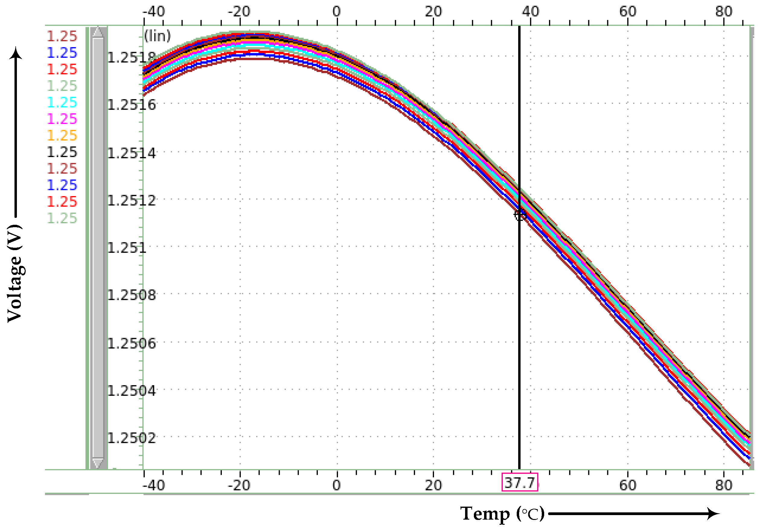
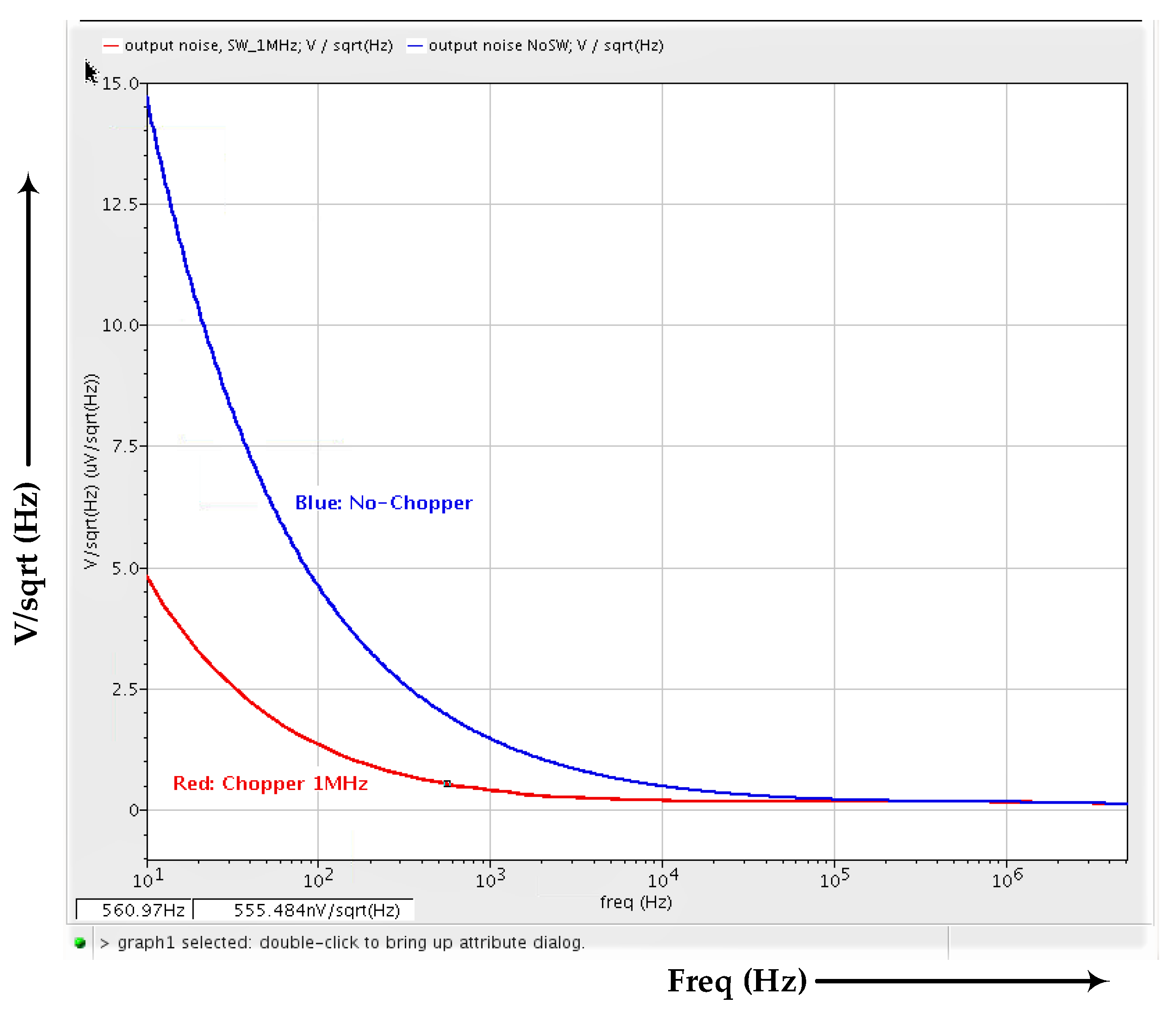
4. Composite BGR Frequency Domain Noise Analysis Results

Frequency domain, as well as time domain noise analysis, was performed for the chopper-enabled composite BGR circuit. Figure 16 shows the noise reduction analysis with and without the chopper scheme simulation graph in the frequency domain. The noise analysis of the composite BGR was evaluated through cadence periodic steady-state (PSS) analysis and periodic noise (PNoise) analysis. The flicker noise was reduced from 1.5 to 0.4 μV/sqrt(Hz) at 1 KHz using chopping techniques. Figure 17 shows that further improvement can be achieved with a filter application in the composite BGR architecture.
The graph shows a reduction in flicker noise from 181.3 to 10.26 mV/sqrt(Hz) at 100 KHz with a filter.

5. Conclusions

In this paper, a high-performance chopper-embedded BGR architecture was presented to suppress low-frequency and offset noise. The complete architecture was realized through 0.18 μm CMOS technology with a startup and a power-down circuit for good accuracy. The BGR circuit generated a reference voltage of 1.25 V, with a supply voltage range of 2.5–3.3 V. The operational transconductance amplifier (OTA) achieved a gain of 84.1dB. The chopper stabilization technique greatly reduced the critical low-frequency noise in comparison to the BGR without a chopper. A non-overlapping clock circuit was also implemented to suppress the clock skew effect. The low-frequency flicker noise was reduced from 1.5 to 0.4 μV/sqrt(Hz) at 1 KHz with the proposed chopping scheme in the bandgap. Comparisons of the noise performance of the chopper-embedded BGR with and without a low-pass filter were also performed, and the results show a further reduction in the overall noise. A reduction in flicker noise from 181.3 to 10.26 mV/sqrt(Hz) at 100 KHz was observed with the filter. Biasing noise analysis also showed a significant reduction in noise by using the proposed chopper-embedded BGR scheme. Hence, the proposed architecture is highly effective in reducing the noise of the clock generators.

Author Contributions

Conceptualization, N.A. (Neeru Agarwal); formal analysis, N.A. (Neeraj Agarwal); methodology, N.A. (Neeru Agarwal) and N.A. (Neeraj Agarwal); supervision, C.-W.L.; validation, C.-W.L.; visualization, M.O.; writing—original draft, N.A. (Neeru Agarwal); writing—review and editing, N.A. (Neeraj Agarwal) and C.-W.L. All authors have read and agreed to the published version of the manuscript.

Funding

This work was supported, in part, by grants from the Ministry of Science and Technology, Taiwan, under Grants MOST 108-2221-E-007-094-MY2, 108-2622-M-007-006-CC1 and 109-2622-M-007-007-CC1.

Acknowledgments

The authors express their best thanks to TYRAFOS Technology Company Ltd., Taiwan, for providing facilities and continuous encouragement, constant help and anonymous reviews about the manuscript. We are also thankful to the Chip Implementation Center (CIC), Taiwan, for their EDA tools, facility and technology support.

Conflicts of Interest

The authors declare no conflict of interest.

References

  1. Razavi, B. Design of Analog CMOS Integrated Circuits, 1st ed.; McGraw-Hill: New York, NY, USA, 2002. [Google Scholar]
  2. Gray, P.; Hurst, P.J.; Lewis, S.H.; Meyer, R.G. Analysis and Design of Analog Integrated Circuits, 4th ed.; John Willey & Sons: New York, NY, USA, 2001. [Google Scholar]
  3. Bakker, A.; Thiele, K.; Huijsing, J.H. A CMOS nested-chooper instrumentation amplifier with 100-nV offset. IEEE J. Solid-State Circuits 2000, 35, 1877–1883. [Google Scholar] [CrossRef]
  4. Razavi, B. Phase-Locked Loops, Design of Analog CMOS Integrated Circuit, 2nd ed.; McGraw Hill Education Private Limited: New York, NY, USA, 2002; pp. 532–576. [Google Scholar]
  5. Sanborn, K.; Ma, D.; Ivanov, V. A sub-1-V low-noise bandgap voltage reference. IEEE J. Solid-State Circuits 2007, 42, 2466–2481. [Google Scholar] [CrossRef]
  6. Um, J.-Y. Calibration of bandgap voltage reference using chopping technique and IIR filter. Electron. Lett. 2016, 52, 1104–1106. [Google Scholar] [CrossRef]
  7. Yu, C.; Siek, L. An area-efficient current-mode bandgap reference with intrinsic robust start-up behavior. IEEE Trans. Circuits Syst. II Express Briefs 2015, 62, 937–941. [Google Scholar] [CrossRef]
  8. Chen, H.M.; Lee, C.C.; Jheng, S.H.; Chen, W.C.; Lee, B.Y. A sub-1 ppm/°C precision bandgap reference with adjusted temperature curvature compensation. IEEE Trans. Circuits Syst. I Regul. Pap. 2017, 64, 1308–1317. [Google Scholar] [CrossRef]
  9. Roh, H.D.; Roh, J.; Duanquanzhen, Q.D. All MOS transistors bandgap reference using chopper stabilization technique. In Proceedings of the 2010 International SoC Design Conference, Incheon, Korea, 22–23 November 2010; pp. 353–357. [Google Scholar] [CrossRef]
  10. Li, C.; Han, B.; Guo, Z.; Wu, L. High-Precision Bandgap Voltage Generation Method with Chopper Stabilization Technique. In Proceedings of the 2019 IEEE International Conference on Electron Devices and Solid-State Circuits (EDSSC), Xi’an, China, 12–14 June 2019; pp. 1–3. [Google Scholar] [CrossRef]
  11. Hayatleh, K.; Lidgey, F.J.; Parta, S. Degradation mechanisms in operational amplifier precision rectifiers. IEEE Trans. Circuits Syst. I Fundam. Theory Appl. 1995, 42, 479–485. [Google Scholar] [CrossRef]
  12. Ming, X.; Ma, Y.-Q.; Zhou, Z.-K.; Zhang, B. A high-precision compensated CMOS bandgap voltage reference without resistors. IEEE Trans. Circuits Syst. II Express Briefs 2010, 57, 767–771. [Google Scholar] [CrossRef]
  13. Banba, H.; Shiga, H. A CMOS Bandgap Reference Circuit with Sub I-V operation. IEEE J. Solid-State Circuits 1999, 34, 670–674. [Google Scholar] [CrossRef] [Green Version]
  14. Hunter, B.L.; Matthews, W.E. A ±3 ppm/°C single-trim switched capacitor bandgap reference for battery monitoring applications. IEEE Trans. Circuits Syst. I Regul. Pap. 2017, 64, 777–786. [Google Scholar] [CrossRef]
  15. Nagulapalli, R.; Palani, R.K.; Bhagavatula, S. A 24.4 ppm/°C Voltage Mode Bandgap Reference with a 1.05 V Supply. IEEE Trans. Circuits and Syst. II Express Briefs 2021, 68, 1088–1092. [Google Scholar] [CrossRef]
  16. Agarwal, N.; Agarwal, N.; Lu, C.-W.; Oh-e, M. A 33 MHz Fast-Locking PLL with Programmable VCO and Automatic Band Selection for Clock Generator Application. Electronics 2021, 10, 1743. [Google Scholar] [CrossRef]
  17. Yang, X.; Chan, C.-H.; Zhu, Y.; Martins, R.P. Calibration-Free Ring-Oscillator PLL with Gain Tracking Achieving 9% Jitter Variation Over PVT. IEEE Trans. Circuits Syst. I Regul. Pap. 2020, 67, 3753–3763. [Google Scholar] [CrossRef]
  18. Jang, T.; Jeong, S.; Jeon, D.; Choo, K.D.; Sylvester, D.; Blaauw, D. A noise reconfigurable all-digital phase-locked loop using a switched capacitor-based frequency-locked loop and a noise detector. IEEE J. Solid-State Circuits 2018, 53, 50–65. [Google Scholar] [CrossRef]
  19. Yu, X.-P.; Fang, Y.; Shi, Z. 2.5 mW 2.73 GHz non-overlapping multiphase clock generator with duty-cycle correction in 0.13 μm CMOS. Electron. Lett. 2016, 52, 1261–1262. [Google Scholar] [CrossRef]
  20. Zhou, Z.-K.; Shi, Y.; Wang, Y.; Li, N.; Xiao, Z.; Wang, Y.; Liu, X.; Wang, Z.; Zhang, B. A Resistor less High-Precision Compensated CMOS Bandgap Voltage Reference. IEEE Trans. Circuits Syst. I Regul. Pap. 2019, 66, 428–437. [Google Scholar] [CrossRef]
  21. Chi-Wa, U.; Zeng, W.-L.; Law, M.-K.; Lam, C.-S.; Martins, R.P. A 0.5-V Supply, 36 nW Bandgap Reference with 42 ppm/°C Average Temperature Coefficient Within −40 °C to 120 °C. IEEE Trans. Circuits Syst. I Regul. Pap. 2020, 67, 3656–3669. [Google Scholar]
  22. Ming, X.; Hu, L.; Xin, Y.-L.; Zhang, X.; Gao, D.; Zhang, B. A High-Precision Resistor-Less CMOS Compensated Bandgap Reference Based on Successive Voltage-Step Compensation. IEEE Trans. Circuits Syst. I Regul. Pap. 2018, 65, 4086–4096. [Google Scholar] [CrossRef]
  23. Zhu, G.; Yang, Y.; Zhang, Q. A 4.6-ppm/°C high-order curvature compensated bandgap reference for BMIC. IEEE Trans. Circuits Syst. II Express Briefs 2019, 66, 1492. [Google Scholar] [CrossRef]
  24. Kamath, U.; Cullen, E.; Yu, T.; Jennings, J.; Wu, S.; Lim, P.; Farley, B.; Staszewski, R.B. A 1-V bandgap reference in 7-nm FinFET with a programmable temperature coefficient and inaccuracy of ±0.2% from −45 °C to 125 °C. IEEE J. Solid-State Circuits 2019, 54, 1830–1840. [Google Scholar] [CrossRef]
  25. Chen, K.; Petruzzi, L.; Hulfachor, R.; Onabajo, M. A 1.16-V 5.8-to-13.5-ppm/°C Curvature-Compensated CMOS Bandgap Reference Circuit With a Shared Offset-Cancellation Method for Internal Amplifiers. IEEE J. Solid State Circuits 2021, 56, 267–276. [Google Scholar] [CrossRef]
Figure 1. Block diagram of the chopper-stabilized BGR noise reduction scheme.
Electronics 10 02257 g001
Figure 2. Chopper-stabilized operational amplifier circuit of the BGR.
Electronics 10 02257 g002
Figure 3. (a) Bandgap reference circuit with an embedded chopper circuit; (b) implementation of highly matched resistors for the BGR scheme.
Electronics 10 02257 g003
Figure 4. Stabilized BGR output with a startup circuit.
Electronics 10 02257 g004
Figure 5. Bandgap reference op amplifier gain and phase margin analysis.
Electronics 10 02257 g005
Figure 6. Non-overlapping clock generator.
Electronics 10 02257 g006
Figure 7. Non-overlapping clock circuit simulation graph.
Electronics 10 02257 g007
Figure 8. Schematic of the chopper circuit.
Electronics 10 02257 g008
Figure 9. (a) Output Vbg without the chopper circuit; (b) output Vbg with the chopper circuit.
Electronics 10 02257 g009
Figure 10. Variation in Vbg over a wide temperature range.
Electronics 10 02257 g010
Figure 11. (a) Variable low-pass filter for current source; (b) variable low-pass filter for cascode devices.
Electronics 10 02257 g011
Figure 12. (a) Switched capacitor resistor; (b) non-overlapping clock; (c) low-pass filter.
Electronics 10 02257 g012
Figure 13. Clock generator bias circuit using the BGR composite scheme.
Electronics 10 02257 g013
Figure 14. Chopper-embedded BGR and sub-block layout (285.25 μm × 125.38 μm).
Electronics 10 02257 g014
Figure 15. BGR with bias circuit sub-block layout (423.765 μm × 315.825 μm).
Electronics 10 02257 g015
Figure 16. Noise comparisons between chopped and non-chopped bandgaps.
Electronics 10 02257 g016
Figure 17. Noise reduction simulation graph for the chopped bandgap with a filter and without a filter.
Electronics 10 02257 g017
Table 1. Summary of component dimensions of the proposed BGR architecture.
ComponentParameter
M1W = 10 µm, L = 4 µm, m = 8
M2W = 10 µm, L = 1 µm, m = 8
M3W = 10 µm, L = 1 µm, m = 2
M4W = 10 µm, L = 1 µm, m = 2
M5W = 10 µm, L = 4 µm, m = 2
M6W = 10 µm, L = 1 µm, m = 2
R17.2 kΩ
R240 kΩ
R340 kΩ
R42 kΩ
R52 kΩ
R62 kΩ
R710 kΩ
R8250 Ω
Table 2. Summary of the operational amplifier PVT analysis.
S.N.TTSSFF
Vdd (Voltage)3.3 V2.97 V3.63 V
Temp (°C)50125−40
Gain (dB)84.180.0689.12
PM (Degree)59.4855.5766.52
Table 3. Summary of the operational amplifier noise analyses.
S.N.TTSSFF
Vdd (Voltage)3.3 V2.97 V3.63 V
Temp (°C)50125−40
Freq = 1 KHz7.89574 μV7.131022 μV6.676753 μV
Freq = 10 KHz92.72738 nV67.98714 nV118.9222 nV
Freq = 100 KHz143.3527 pV95.01332 pV195.6376 pV
Table 4. Summary of the pre- and post-simulations.
Chopper EnabledPre_TTPost_TT
VoltagePrePost
Vbg1.2314 V1.2302 V
Vbp11.9474 V1.9428 V
Vbp21.1281 V1.1232 V
Vbp1_filter1.9474 V1.9428 V
Vbp2_filter1.1281 V1.1232 V
Table 5. Summary of bias circuit current pre-simulation analysis.
CurrentTT/3.3 V/50 °CSS/2.97 V/125 °CFF/3.63 V/−40 °C
3.75 μA3.7872 μA3.4434 μA4.1977 μA
7.5 μA7.6112 μA6.9713 μA8.3593 μA
15 μA15.253 μA14.021 μA16.675 μA
30 μA30.505 μA28.0424 μA33.348 μA
60 μA61.009 μA56.083 μA66.692 μA
Table 6. Summary of bias circuit current post-simulation analysis.
CurrentTT/3.3 V/50 °CSS/2.97 V/125 °CFF/3.63 V/−40 °C
3.75 μA3.8868 μA3.52155 μA4.3288 μA
7.5 μA7.8594 μA7.16935 μA8.682 μA
15 μA15.1114 μA13.9025 μA16.497 μA
30 μA30.4494 μA27.9886 μA33.284 μA
60 μA60.4294 μA55.5984 μA65.962 μA
Table 7. Performance summary and comparison with other bandgap reference circuits.
TypeProposed[12][14][20][22][23]
Supply voltage (V)2.83.65.226~52.5~53.5–5
Vbg (V)1.251.233.651.141.1963.11
Temp range (°C)−40~125−40~120−40~100−40~125−10~130−40~130
Trimming methodNo-trimYesSingle-trimMulti-trimMulti-trimYes
Current consumption (μA)301807503338108
Min TC (ppm/°C)4.3611.831.013.984.6
Line regulation(mV/V)N.A.N.A.N.A.20.190.31
PSRR (dB)−68.8−31.8−127−61−84−74
Chip area (mm2)
Technology
0.03
0.18 μm CMOS
0.1
0.13 μm CMOS
0.28
0.18 μm Bi CMOS
0.04
0.35 μm CMOS
0.053
0.5 μm CMOS
0.223
0.18 μm CMOS
Publisher’s Note: MDPI stays neutral with regard to jurisdictional claims in published maps and institutional affiliations.

