Article

A Balanced Filtering Directional Coupler with Wide Common-Mode Suppression Based on Slotline Structure

1
National Key Laboratory of Antennas and Microwave Technology, Xidian University, Xi’an 710071, China
2
Beijing Institute of Spacecraft Environment Engineering, Beijing 100094, China
*
Author to whom correspondence should be addressed.
Electronics 2021, 10(18), 2254; https://doi.org/10.3390/electronics10182254
Submission received: 11 August 2021 / Revised: 7 September 2021 / Accepted: 9 September 2021 / Published: 14 September 2021
(This article belongs to the Special Issue Novel Microwave/Millimeter-Wave Devices and Antennas)

Abstract

:
In this paper, a balanced-to-balanced filtering directional coupler (FDC) that can realize a 3 dB coupling degree directional coupler with high isolation and directivity is proposed. The design of the proposed FDC is primarily based on microstrip/slotline transition structures, resonance structures, and odd–even mode phase velocity compensation structures. A U-type microstrip feed line integrated with a stepped-impedance slotline resonator is adopted at the input and output ports, which makes the differential-mode (DM) responses independent of the common-mode (CM) ones, and brings superior DM transmission and CM suppression. In addition, by loading the microstrip stub-loaded resonators (SLRs), a DM passband with sharp filtering performance is realized, and transmission zeros (TZs) can be added into the design, which makes it more selective. Moreover, phase compensating slotlines are added into the coupling structure to enhance the isolation. In order to verify the feasibility of the proposed design method, an FDC prototype circuit was made and tested. The simulation results are in good agreement with the measured results. The designed coupler’s DM operating band covers 2.65 GHz to 3 GHz (FBW = 12.4%), and the insertion and return losses are 4.6 dB and 20 dB, respectively. The isolation degree is better than 15 dB, and the CM suppression is more than 55 dB. The total coupler size is about 67.7 mm × 63.8 mm. The designed balanced-to-balanced FDC can be widely used in S-band wireless communication systems.

Graphical Abstract

1. Introduction

In recent years, with the development of small-scale integration, RF and microwave systems require more integrated circuits and devices. Directional couplers, as an indispensable part of RF circuits, have been paid more and more attention because of their unique performance of high directivity and power distribution of microwave signals in a certain proportion. In [1], the short-circuit coupling line was placed in the conventional coupler to strengthen the coupling, but this reduced the bandwidth. Inserting left/right composite elements [2] into the directional coupler could improve the coupling degree, but the directivity will worsen. A fragment compensation structure was used in [3] to improve the directivity of the coupler, but at the expense of bandwidth. In [4], a directional coupler was designed using slotlines, but the CM suppression was poor.
Balanced/differential structures were widely used in RF passive devices because they can effectively suppress CM impedance [5,6,7,8]. In [9], a broadband CM suppression filter was added at the excitation end to suppress the common mode. In [10], by introducing a multilayer dielectric structure and placing the sections on different metallized layers, different coupling coefficients required for each coupling line section were realized. The model works in the differential mode, and the common mode rejection is high.
Filters were widely used in RF circuits and have been paid much attention in recent years [11,12,13]. Ref. [14] presents a balanced passband filter (BPF) with independently tunable/controllable dual passbands, using element-loaded, stepped-impedance resonators (SIRs). Ref. [15] designed a DM wideband BPF with enhanced CM suppression by using a slotline resonator.
Device miniaturization can be realized by combining the coupler with the filter. By combining the power directional coupler in the reflection mode, a filter with a wide band width was proposed by [16]. In [17], the aperture was set on the ground plane by using slotline technology, and the filter structure was optimized using the coupling line; this greatly improves the filtering characteristics, but the selectivity is low. Ref. [18] used the branch line coupler as the transverse filtering part; the out-of-band response was synthesized by loading the coupling port of the coupler and taking the isolation port as the output node. As far as the current research shows, there are few reports of differential filtering directional couplers.
In this paper, a novel balanced-to-balanced FDC is proposed and analyzed. The couplers operate at a frequency of 2.3–3.3 GHz, and can be widely used in microwave systems such as radio frequency identification (RFID), wireless local area networks (WLAN), and global interoperability of microwave access (WiMAX). The coupler adopts a U-type microstrip feed line integrated with a stepped-impedance slotline resonator, as shown in Figure 1a (1), which can separate CM and DM, and effectively improve CM suppression. Two SLRs are introduced to increase the selectivity in the bandwidth, as shown in Figure 1a (2). An L-junction slotline for impedance matching has been designed. Under the condition that the power distribution is equal, the introduction of zeros is added to further improve the selectivity. In addition, in the structure of the coupler, the slotline is used to separate the even mode from the odd mode, as shown in Figure 1a (3). Since the phase velocity of the even mode and the odd mode are different, increasing the size length of the slotline can effectively compensate the phase velocity, thus enhancing the isolation and directivity.
Compared with its predecessors, this paper has the following advantages: Firstly, a U-type microstrip transition gap structure is proposed to enhance CM suppression. Secondly, an SLR structure is added to enhance the selectivity of the model. Thirdly, two TZs, low-frequency TZ and high-frequency TZ, are introduced to make the zeros appear on both sides of the frequency band, effectively isolating the clutter outside the band, and further strengthening the selectivity of the model. The CM rejection in the passband is greater than 55 dB, and the DM isolation degree is greater than 20 dB. The rest of the paper is organized as follows: In the second part, the performance of the designed directional coupler with filter structure is analyzed. In the third part, the simulation and test results of the high-selectivity directional coupler with filter structure are analyzed. The fourth part is a summary of the full text.

2. Balanced-to-Balanced Filtering Directional Coupler

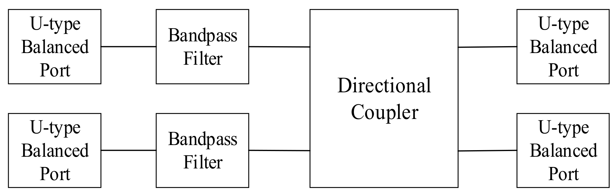
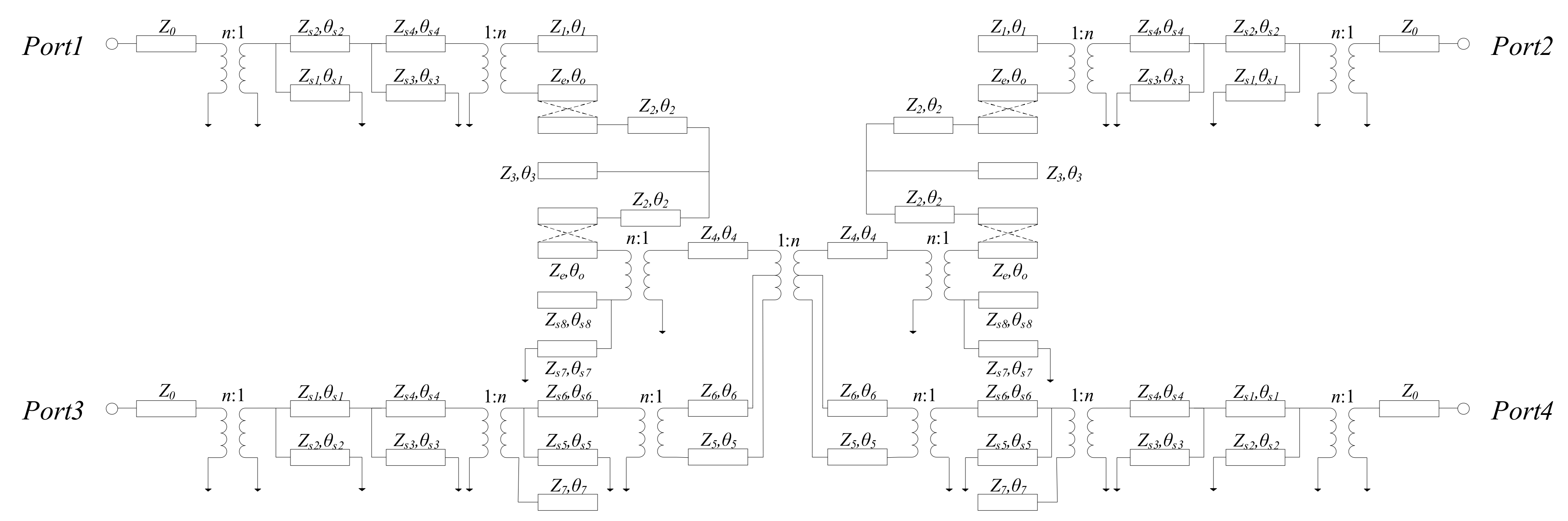
2.1. Overall Design Principles and Ideas

Slotlines are a technique in which narrow slits are etched into one side of the grounding metal layer of the dielectric substrate. Their geometry is flat, making them ideal for use in microwave circuits. The structure diagram of the designed highly selective directional coupler with filtering structure is shown in Figure 1, which consists of U-type microstrip-to-slotline structures (described in Section 2.2), filtering resonance structures (described in Section 2.3), L-type slotline structures (described in Section 2.4), and odd–even mode phase speed compensation structures (described in Section 2.5). Figure 2 shows an internal schematic of the designed coupler. As can be seen from the figure, the coupler designed in this paper can be simply obtained, by cascading two SLRs and a coupler at the output port and coupling port.
The circuit schematic diagram of the designed FDC working in DM mode is shown in Figure 3. Where Zn (n = 0, 1, 2, 3, 4, 5, 6, 7) represents the characteristic impedance of the microstrip line, Zsn (n = 1, 2, 3, 4, 5, 6, 7, 8) represents the characteristic impedance of the slotline, and Ze and Zo, respectively, represent the even-model impedance and the odd-model impedance of the parallel coupling line. θn (n = 1, 2, 3, 4, 5, 6, 7) and θsn (n = 1, 2, 3, 4, 5, 6, 7, 8) denote the electric length of microstrip line and slotline, respectively, where θn = 2πln/λn, θsn = 2πlsn/λsn (n = 1, 2, 3, 4, 5, 6, 7, 8). (λn is the guided wavelength of microstrip line at the center frequency of the proposed FDC, λsn is the guided wavelength of slotline at the center frequency of the proposed FDC.)
The scattering matrix of an ideal directional coupler is as follows:
[ S ] = 0 α j β 0 α 0 0 j β j β 0 0 α 0 j β α 0
An ideal directional coupler is characterized by matching at all ports, while a multi-section stepped symmetrical directional coupler can be regarded as a quarter-wavelength stepped impedance filter. The ABCD matrix of the prototype circuit of n section quarter-wavelength stepped impedance filter is:
A n j B n j C n D n = i = 1 n cos θ j Z i sin θ j sin θ Z i cos θ
according to the transformation relationship between S parameter matrix and ABCD matrix, the attenuation coefficient of the circuit can be obtained as:
L A = 1 + 1 4 ( A n B n ) 2 + 1 4 ( B n C n ) 2
since An = Bn, the attenuation coefficient is:
L A = 1 + P n 2 ( sin θ )
For matches at each port, the odd–even mode impedance at each point of the coupling line is as follows:
Z 0 e Z 0 o = Z o 2
Therefore, the coupling line impedance can be obtained only by calculating the even- mode impedance. The calculation impedance synthesis process is as follows [19]:
| Γ | 2 = P n 2 ( x ) 1 + P n 2 ( x )
x = s / j 1 + ( s / j ) 2 = sin θ
where s/j = tanθ.
Therefore, the impedance function is:
Z ( s ) = 1 + Γ 1 Γ
If the ABCD matrix is left multiplied by a matrix and an expression, the new ABCD matrix and the impedance of each coupling line can be obtained as follows:
1 1 s 2 1 Z n s s Z n 1 A B C D = A ¯ B ¯ C ¯ D ¯
where Zn = As/Cs|s=n−1.
Repeat the above calculation formula to calculate the impedance of each coupling line.
Microstrip/slot transition structures can be represented by equivalent transformers. Transformer turn ratio n represents the coupling amplitude between microstrip line and slotline. When the RF signal is excited from the balanced input port, the DM signal is transferred into the slotline through the U-type microstrip feeder, and reaches the filtering part through the underlying L-junction gap structure. Since part of the energy is coupled from the lower symmetric L-junction slotline, and the other part is coupled to the upper SLR, the two energy channels have the same amplitude and the phase difference is 180°, resulting in a sharp pass band, which enhances the out-of-band suppression effect and greatly improves the model selectivity.
The length of the coupling part is selected as a quarter wavelength of the central frequency. Because the phase velocities of odd mode and even mode are different, the directivity of the coupler will be affected. By increasing the length of the slotline, the low phase of the odd mode is compensated. After the signal enters the coupler part, the odd-mode signal is separated and transmitted forward along the slotline, while the even-mode signal remains unchanged. Then, the odd mode with compensated phase is coupled from the slotline to the microstrip line, and energy is the output from the coupling end. The following sections provide an introduction to each of these.
The frequency response coming from the equivalent circuits is calculated using the Advanced Design System (ADS), as shown in Figure 4. Compared with the results of HFSS, a good agreement is obtained to verify the equivalent circuit. It can be seen from the figure that ADS corresponds well with HFSS simulation results: both frequency bands are around 2.2 GHz − 3.3 GHz, and the transmission zeros’ positions are around 2.3 GHz and 3.3 GHz, respectively. In the DM passband, the return loss is better than 13 dB, the minimum coupling of DC is 4.69 dB, the maximum coupling is 5.20 dB, and the isolation degree is better than 15 dB. The characteristics and selectivity of the coupler in ADS and HFSS are consistent.

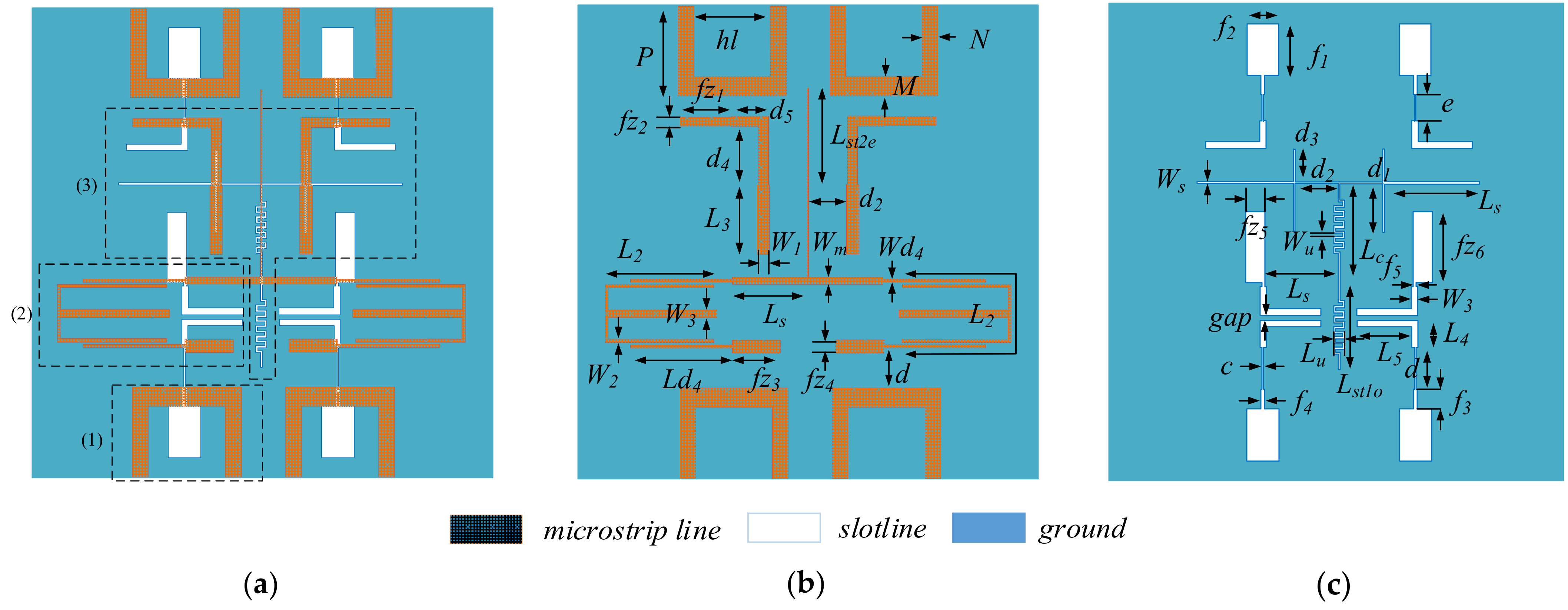
2.2. Balanced Microstrip/Slotline Transition Structure

The proposed FDC consists of four U-type microstrip/slotline feeders located at each of its four port positions. Each balanced microstrip/slot structure consists of a U-type stepped-impedance microstrip feedline and a stepped-impedance slot resonator. The stepped-impedance slot resonator is etched on the bottom metal layer, and the U-type microstrip is located on the upper layer of the dielectric plate, perpendicular to the step impedance slot resonator. The slotline extends forward about a quarter wavelength size, while the quarter wavelength microstrip line is also required for impedance matching above. The U-type microstrip line is coupled with the slotline by a magnetic field.
Because of the symmetry of the circuit structure, the odd–even mode separation method can be used to analyze the transition gap structure of the balanced microstrip. Figure 5 shows the U-type balanced microstrip/slotline transition structure.
When the DM signal enters, a virtual electric wall is generated at the center of slotline A-A’, as shown in Figure 6a. The DM signal can pass through the virtual electric wall, so it can be transmitted further. When the CM signal enters, a virtual magnetic wall is generated at the center A-A’ of the slotline, as show in Figure 6b. As the magnetic wall perpendicular to the electric field conflicts with the boundary conditions of the magnetic wall, the CM signal cannot pass through. Therefore, the CM signal is inhibited without affecting the DM signal. The balance microstrip transition gap structure can effectively save the size, under the condition of ensuring the function.

2.3. Filter Resonant Structure

SLR consists of a half-wavelength microstrip resonator and an open-circuit sub-loaded in the center. The resonant frequency can be changed by adjusting the resonant length of the filter. SLR has a symmetrical structure, as shown in Figure 7a, so it can be analyzed using the odd–even mode analysis method, where Y1, L1, Y2, and L2 represent the characteristic admittance and length of the microstrip line and the open nipples, respectively. The open nipples are shunt in the middle of the microstrip line. When odd-mode excitation enters, a zero voltage value is generated in the middle of the resonator, so the circuit can be equivalent to half of the microstrip resonator, as shown in Figure 7b. When the even-mode excitation enters, no current flows through the middle of the resonator, so it can be regarded as an open circuit. The equivalent circuit diagram is shown in Figure 7c.
Therefore, the odd-mode and even-mode resonant frequencies can easily be:
f o d d = ( 2 n 1 ) c 2 L 1 ε e f f
f e v e n = n c ( L 1 + 2 L 2 ) ε e f f
where n = 1, 2, 3, …, c is the speed of light in free space, and εeff denotes the effective dielectric constant of the substrate.
It can be observed that the odd-mode resonant frequencies are not affected by the open stub, and the center frequency fc can be roughly expressed as:
f c = f 1 + f 2 2
Therefore, the center frequency and fractional bandwidth (FBW) of the proposed FDC are controllable and can be adjusted easily.

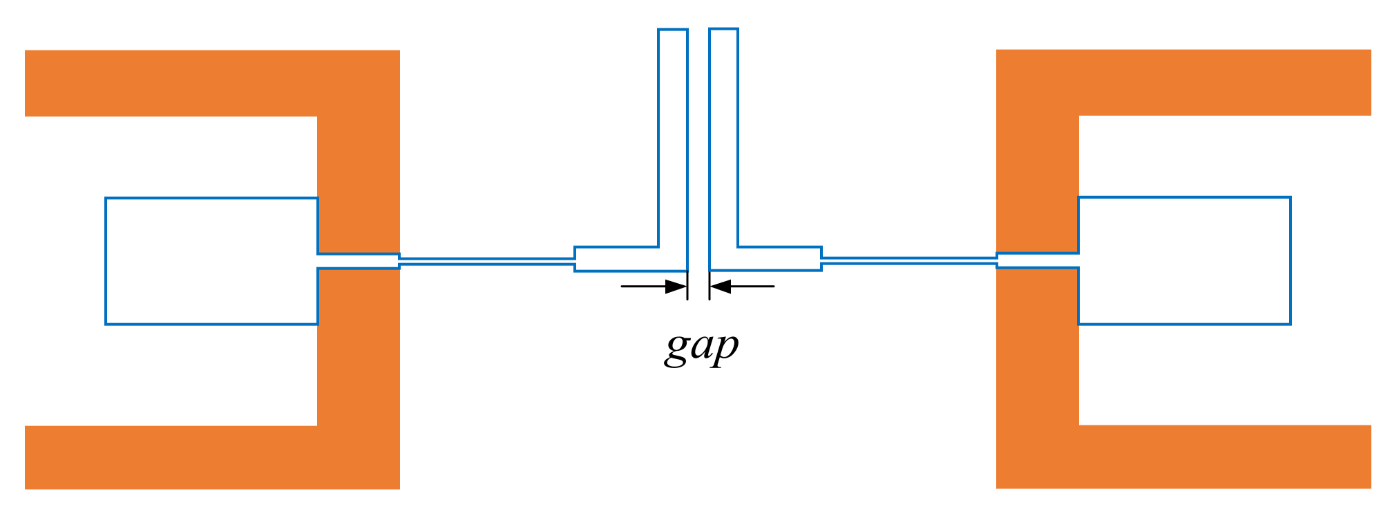
2.4. L-Junction Slotlines and Transmission Zeros

Figure 8 shows the L-junction symmetric slot structure used. The symmetrical L-junction slotlines can be coupled with energy. When the energy is excited from the input port, part of the energy is transmitted from the microstrip line to the microstrip part at the right end of the SLR structure. Another part of energy from the input port is transmitted through the lower L-junction slotline, coupled to the symmetric L-junction slotline, and then coupled to the upper microstrip line.
At this point, the energy of the two channels is of the same amplitude, and the phase difference is 180°, resulting in the low-frequency TZ. The reason for TZ is that when the signal reaches the load through multiple transmission paths, the phase of each transmission path is different, and the superposition of 180° opposite phases occurs at a specific frequency point, resulting in TZ.
The change of TZ point position is affected by the spacing between the symmetric L-junction slotline. The second reason for TZ is the inherent nature of SLR.
The introduction of two TZs can effectively improve the passband selectivity. The low-frequency TZs are affected by the symmetrical L-junction slotline distance, and the TZ1 position can be controlled by changing the spacing between slotlines and the SLR microstrip structure length, as shown in Figure 9a,b. The location of the TZ2 is determined by the length of the SLR central opening short, as shown in Figure 9c. As can be seen, when the length of L2 is changed, the position of TZ2 will change, while the position of TZ1 will not be affected.

2.5. Odd–Even Mode Phase Velocity Compensation Structures

The phase velocity of odd and even modes is different because of the different dielectric constant. The isolation of the coupler deteriorates due to the gap between the parity mode phase velocity. In order to improve the performance of the coupler, the designed balanced-to-balanced FDC proposes an odd–even mode phase velocity compensation structure with multiple U-shaped bending slotlines. The compensation structure compensates the odd-mode phase velocity by lengthening the slotline. In order to save size, the slotline is designed as a U-shaped bending structure. By increasing the slotline of the U-shaped bending structure, the odd–even mode phase velocity can be compensated effectively, and the isolation degree of the coupler can be improved significantly. Figure 10a shows the coupling part with no even-mode phase velocity compensation structure. Figure 10b shows the coupling part of the single-phase velocity compensation structure. Figure 10c shows the coupling part of the dual-phase velocity compensation structure. The simulation results are compared as shown in Figure 11. It can be seen from the figure that after adding the multi-U-type parity mode phase velocity compensation structure, the isolation of the balanced-to-balanced FDC is significantly improved.

2.6. Design Procedure

Based on the above analysis and discussion, a simple design procedure of the proposed balanced-to-balanced FDC can be summarized as follows:
Step 1: According to (1) and (5), realizable electrical lengths and characteristic impedances of microstrip lines and slotlines can be chosen.
Step 2: According to (6) and (9), the ABCD parameter matrix of the coupler is defined, and the performance of the coupler is further understood.
Step 3: According to (10) and (12), the center frequency and operating bandwidth of the resonant structure can be defined.
Step 4: Further optimize all values to realize better DM and CM responses and isolation performance of the proposed FDC. Full-wave electromagnetic simulation and dimension optimization in the commercial software of HFSS can be conducted.

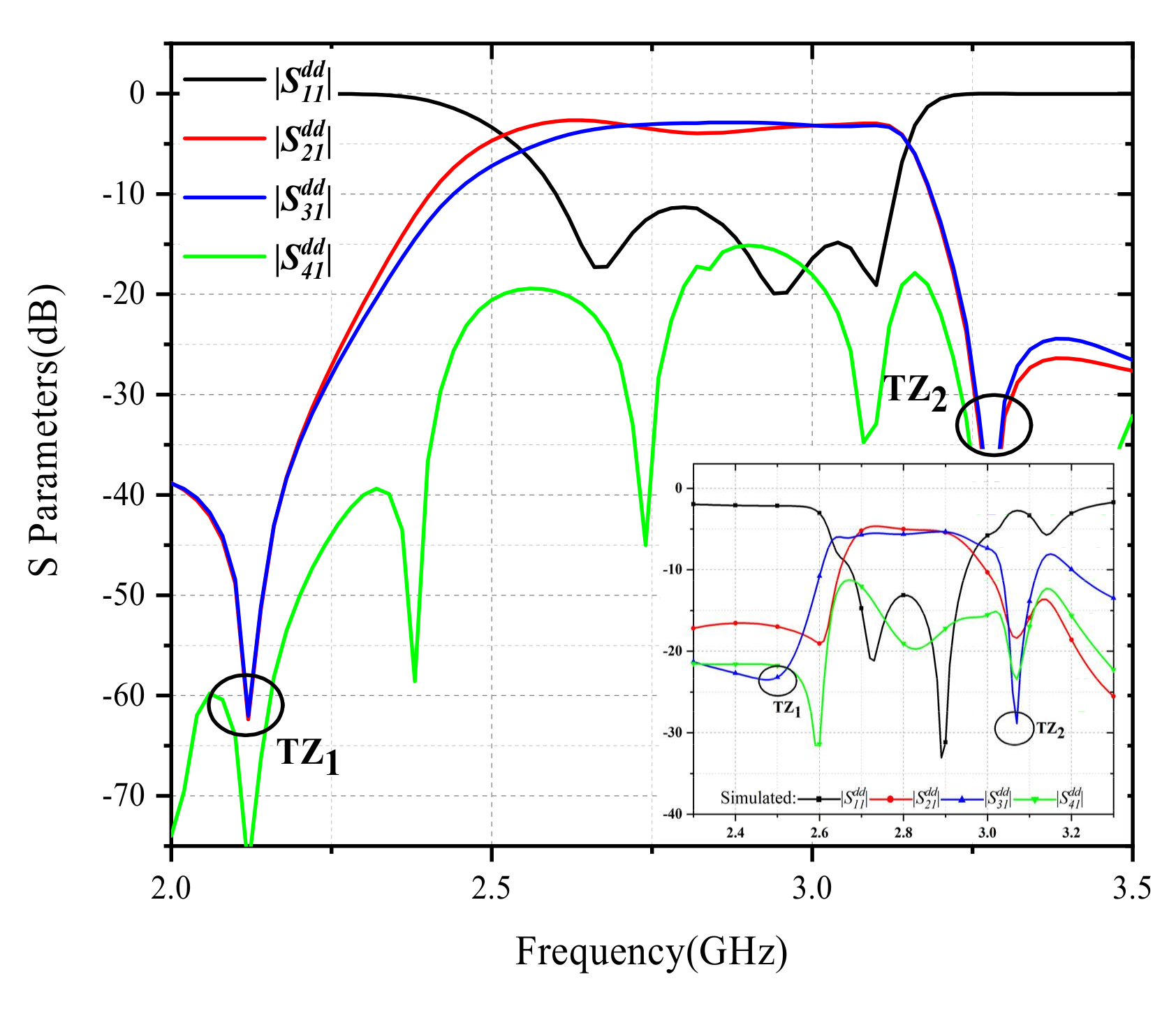
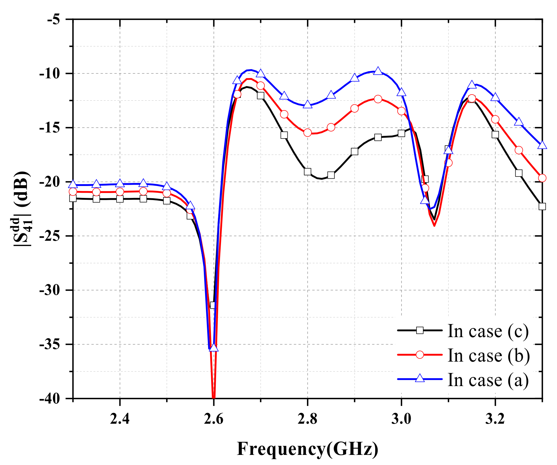
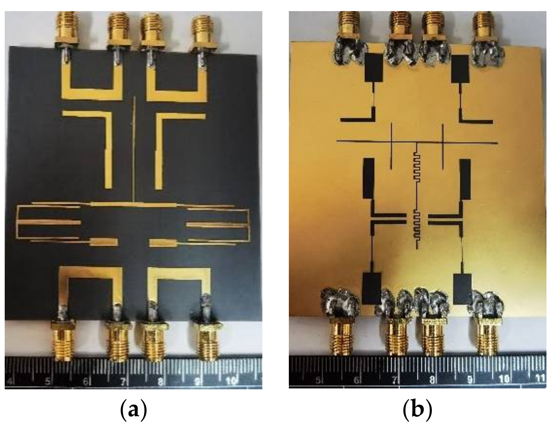
3. Simulation and Measurement Results

The configuration of the proposed FDC is shown in Figure 1a. Photographs of the proposed FDC are shown in Figure 12. To verify the feasibility of this design method, Rogers RT/Duroid5880 substrate was used with a dielectric constant of 2.2, a loss tangent of 0.0009, and a thickness of 0.8 mm. The total size of the design is about 67.70 mm × 63.80 mm(0.59λg × 0.63λg, where λg is the waveguide wavelength at 2.8 GHz), and its size is: Wm = 1.1, Ws = 0.3, Wu = 0.5, Lst1o = 12.9, Lst2e = 14.7, Lc = 14.7, Lu = 1.7, a = 70, b = 73.7, c = 0.2, d = 5, e = 1.6, l = 4, Wm2 = 1.6, W1 = 1.9, d1 = 5, d2 = 8.5, d3 = 7.4, d4 = 8.9, d5 = 5.8, L1 = 42, L2 = 17, L3 = 10.7, L4 = 4.2, L5 = 8.5, Ls = 11.9, hl = 12, M = 3, N = 2.5, P = 14, g = 0.4, Ld4 = 16, Wd4 = W2 = 0.5, W3 = 1.2, fz1 = 8, fz2 = 1.5, fz3 = 7.5, fz4 = 2, fz5 = 3, fz6 = 11, gap = 0.5, f1 = 8, f2 = 5, f3 = 3, f4 = 0.6, f5 = 0.5, all are in millimeters. The S parameters of the proposed and prepared FDC were measured by Agilent VNA (Vector Network Analyzer) N5230. The comparison of simulated and measured DM responses is shown in the figure. It can be seen that near the passband, the measured results are in good agreement with the simulation results. A DM operating band covering 2.65 GHz to 3 GHz (FBW = 12.4%) was obtained. Figure 13a depicts the performance when the input is port 1. In the DM passband, the return loss is better than 13 dB, the minimum coupling of DC is 4.69 dB, the maximum coupling is 5.20 dB, and the isolation degree is better than 15 dB. At the same time, two TZs of 2.49 GHz and 3.07 GHz can be realized, respectively, located on both sides of the pass band. As shown in Figure 13b, in the DM passband range, the CM rejection is better than 55 dB, and the maximum CM rejection is better than 60 dB. CM return reflection is close to 0 dB, which is equivalent to all CM signals being suppressed. At the same time, a good impedance matching of the output ports is realized. It can be seen that high CM suppression (more than 55 dB) was achieved in both simulation and measurement. It can be seen that the CM response is independent of the DM response.
Comparison with some of the previously reported directional couplers is shown in Table 1. It can be seen that the proposed balanced-to-balanced FDC has generally superior performance in isolation, selectivity, and CM inhibition. Better performance and a simpler structure make it an attractive and competitive FDC in balanced wireless communication systems.

4. Conclusions

In this paper, a balanced-to-balanced differential filtering directional coupler with superior performance is designed and analyzed. The characteristics of this balanced-to-balanced FDC are fabricated and measured. The simulated results and the measured results agree very well. The simulated and measured results indicate that the proposed balanced-to-balanced FDC has the advantages of obvious CM suppression effect, good isolation of DM in the passband, and high selectivity. The designed coupler’s DM operating band covers 2.65 GHz to 3 GHz (FBW = 12.4%), the insertion and return losses are 4.6 dB and 20 dB, respectively, the CM suppression is better than 55 dB, and the CM return reflection is close to 0 dB. The total coupler size is about 67.7 mm × 63.8 mm. Moreover, the proposed balanced-to-balanced FDC can be used in a variety of balancing circuits, such as radio frequency identification (RFID), wireless local area networks (WLAN), and global interoperability of microwave access (WiMAX).

Author Contributions

L.Q. designed and fabricated the proposed structure. F.W. and L.Q. measured the couplers and wrote the manuscript. F.W. and L.Q. contributed to the discussion and reviewed the manuscript. F.W. supervised the project and reviewed the manuscript. Y.H., R.L., Y.Y., X.Y. and N.W. supervised the project. All authors have read and agreed to the published version of the manuscript.

Funding

This research was supported by the National Natural Science Foundation of China (61771015).

Conflicts of Interest

The authors declare no conflict of interest.

References

  1. Wu, Y.; Sun, W.; Leung, S.W.P.; Diao, Y.; Chan, K.-H.; Siu, Y.M.T. Single-Layer Microstrip High-Directivity Coupled-Line Coupler with Tight Coupling. IEEE Trans. Microw. Theory Tech. 2013, 61, 746–753. [Google Scholar] [CrossRef]
  2. Caloz, C.; Sanada, A.; Itoh, T. A novel composite right-/lefthanded coupled-line directional coupler with arbitrary coupling level and broad bandwidth. IEEE Trans. Microw. Theory Tech. 2004, 52, 980–992. [Google Scholar] [CrossRef]
  3. Wang, L.; Wang, G.; Sidén, J. High-performance tight coupling microstrip directional coupler with fragment-type compensated structure. IET Microw. Antennas Propag. 2017, 11, 1057–1063. [Google Scholar] [CrossRef]
  4. Nasr, A.M.H.; Safwat, A.M.E. Tightly Coupled Directional Coupler Using Slotted-Microstrip Line. IEEE Trans. Microw. Theory Tech. 2018, 66, 4462–4470. [Google Scholar] [CrossRef]
  5. Deng, H.W.; Han, Y.K.; Sun, L.; Zhu, J.M.; Xing, S.B. Multilayer Dual-Mode Balanced SIW Filter Utilizing PEC–PMC Characteristic for Common-Mode Suppression. IEEE Microw. Wirel. Compon. Lett. 2020, 30, 865–868. [Google Scholar] [CrossRef]
  6. Wang, L.; Shi, J.; Xu, K.; Yin, Z.W. Compact Dual-Strip Coupled Dual-Patch Antenna for Millimeter-Wave AiP Applications. IEEE Antennas Wirel. Propag. Lett. 2021, 20, 577–581. [Google Scholar] [CrossRef]
  7. Zhu, H.; Qin, P.Y.; Guo, Y.J. Single-Ended-to-Balanced Power Divider with Extended Common-Mode Suppression and Its Application to Differential 2 × 4 Butler Matrices. IEEE Trans. Microw. Theory Tech. 2020, 68, 1510–1519. [Google Scholar] [CrossRef]
  8. Li, Y.C.; Xue, Q. Tunable Balanced Bandpass Filter With Constant Bandwidth and High Common-Mode Suppression. IEEE Trans. Microw. Theory Tech. 2011, 59, 2452–2460. [Google Scholar] [CrossRef]
  9. Martel, J.; Fernández-Prieto, A.; del Río, J.L.M.; Martín, F.; Medina, F. Design of a Differential Coupled-Line Directional Coupler Using a Double-Side Coplanar Waveguide Structure With Common-Signal Suppression. IEEE Trans. Microw. Theory Tech. 2021, 69, 1273–1281. [Google Scholar] [CrossRef]
  10. Piekarz, I.; Sorocki, J.; Janisz, K.; Wincza, K.; Gruszczynski, S. Wideband Three-Section Symmetrical Coupled-Line Directional Coupler Operating in Differential Mode. IEEE Microw. Wirel. Compon. Lett. 2018, 28, 488–490. [Google Scholar] [CrossRef]
  11. Shi, J.; Xue, Q. Balanced Bandpass Filters Using Center-Loaded Half-Wavelength Resonators. IEEE Trans. Microw. Theory Tech. 2010, 58, 970–977. [Google Scholar] [CrossRef]
  12. Shi, J.; Xue, Q. Dual-Band and Wide-Stopband Single-Band Balanced Bandpass Filters with High Selectivity and Common-Mode Suppression. IEEE Trans. Microw. Theory Tech. 2010, 58, 2204–2212. [Google Scholar] [CrossRef]
  13. Qiang, J.; Shi, J.; Cao, Q.; Shen, Z. Compact Differential Wideband Bandpass Filters Based on Half-Wavelength Lines. IEEE Microw. Wirel. Compon. Lett. 2017, 27, 906–908. [Google Scholar] [CrossRef]
  14. Chen, J.-X.; Du, M.-Z.; Li, Y.-L.; Yang, Y.-J.; Shi, J. Independently Tunable/Controllable Differential Dual-Band Bandpass Filters Using Element-Loaded Stepped-Impedance Resonators. IEEE Trans. Compon. Packag. Manuf. Technol. 2017, 8, 113–120. [Google Scholar] [CrossRef]
  15. Lu, Y.-J.; Chen, S.-Y.; Hsu, P. A Differential-Mode Wideband Bandpass Filter With Enhanced Common-Mode Suppression Using Slotline Resonator. IEEE Microw. Wirel. Compon. Lett. 2012, 22, 503–505. [Google Scholar] [CrossRef]
  16. Gomez-Garcia, R.; Sanchez-Soriano, M.A.; Sanchez-Renedo, M.; Torregrosa-Penalva, G.; Bronchalo, E. Low-Pass and Bandpass Filters With Ultra-Broad Stopband Bandwidth Based on Directional Couplers. IEEE Trans. Microw. Theory Tech. 2013, 61, 4365–4375. [Google Scholar] [CrossRef]
  17. Liang, C.-H.; Chang, W.-S.; Chang, C.-Y. Enhanced Coupling Structures for Tight Couplers and Wideband Filters. IEEE Trans. Microw. Theory Tech. 2010, 59, 574–583. [Google Scholar] [CrossRef]
  18. Gomez-Garcia, R.; Alonso, J.I.; Amor-Martin, D. Using the branch-line directional coupler in the design of microwave bandpass filters. IEEE Trans. Microw. Theory Tech. 2005, 53, 3221–3229. [Google Scholar] [CrossRef]
  19. Cristal, E.; Young, L. Theory and Tables of Optimum Symmetrical TEM-Mode Coupled-Transmission-Line Directional Couplers. IEEE Trans. Microw. Theory Tech. 1965, 13, 544–558. [Google Scholar] [CrossRef]
  20. Fouda, A.E.; Safwat, A.M.E.; El-Hennawy, H. On the Applications of the Coupled-Line Composite Right/Left-Handed Unit Cell. IEEE Trans. Microw. Theory Tech. 2010, 58, 1584–1591. [Google Scholar] [CrossRef]
  21. Tan, X.; Lin, F.; Sun, H.; Xue, Q. Planar Reconfigurable Balanced Rat-Race Coupler with Improved Amplitude Imbalance Performance and Common-Mode Noise Absorption. IEEE Trans. Microw. Theory Tech. 2020, 68, 4276–4289. [Google Scholar] [CrossRef]
  22. Lin, F. A Planar Balanced Quadrature Coupler with Tunable Power-Dividing Ratio. IEEE Trans. Ind. Electron. 2017, 65, 6515–6526. [Google Scholar] [CrossRef]
Figure 1. Configuration of: (a) The proposed FDC; (b) The top microstrip line structure; (c) The bottom slotline structure.
Electronics 10 02254 g001
Figure 2. Internal schematic illustration of the proposed FDC.
Electronics 10 02254 g002
Figure 3. Transmission-line equivalent circuit of the proposed FDC under DM operation.
Electronics 10 02254 g003
Figure 4. Simulation results of ADS about DM operation.
Electronics 10 02254 g004
Figure 5. U−type balanced microstrip/slotline transition structure.
Electronics 10 02254 g005
Figure 6. Electric fields and magnetic fields in BFDC transition structure under: (a) DM operation; (b) CM operation.
Electronics 10 02254 g006
Figure 7. (a) Configuration of the SLR; (b) Odd-mode equivalent circuit; (c) Even-mode equivalent circuit of SLR.
Electronics 10 02254 g007
Figure 8. L-junction symmetric slot structure.
Electronics 10 02254 g008
Figure 9. (a) Positions of TZ1 with different Ld4; (b) Positions of TZ1 with different gap; (c) Positions of TZ2 with different L2.
Electronics 10 02254 g009
Figure 10. FDC odd–even mode compensation structure under: (a) Uncompensated structure; (b) Single-compensated structure; (c) Double-compensated structure.
Electronics 10 02254 g010
Figure 11. Comparison of isolation degree under three compensation structures.
Electronics 10 02254 g011
Figure 12. Photographs of the proposed FDC: (a) Top; (b) Bottom.
Electronics 10 02254 g012
Figure 13. Comparisons of the simulated and measured results: (a) DM operation; (b) CM suppression and CM return reflection.
Electronics 10 02254 g013
Table 1. Comparison with recently reported balanced-to-balanced FDC.
Ref.Freq (GHz)BW (RL > 10 dB)No. Of TZsCM AbsorptionISO (dB)CMS (dB)Size (λg2)
[4]1.87/3.18522NO28NO0.40 × 0.55
[20]1.30/2.25531NO25NO0.26 × 0.26
[21]1.75/2.25192YES20200.86 × 0.62
[22]1.90/2.1015NONO25400.88 × 0.21
This Work2.30/3.30122YES20550.59 × 0.63
Iso = Isolation; CMS = Common-mode Suppression.
Publisher’s Note: MDPI stays neutral with regard to jurisdictional claims in published maps and institutional affiliations.

