1. Introduction
The class E inverter has found numerous applications in radio transmission, induction heating, industrial ultrasonic, renewable energy systems, or the commercial electronics industry [
1,
2,
3,
4,
5,
6,
7,
8,
9,
10,
11]. The widespread adoption of this inverter is mainly due to the compact structure with low component count and high-power driving capability. On top of that, if coupled with the zero-voltage switching (ZVS) or zero derivative voltage switching (ZVDS) techniques, it can operate with high efficiency even at very high switching frequency. The analytical modeling and design of the ZVS/ZVDS class E inverters are well reported in the literature [
1,
2,
8,
9,
10,
11,
12,
13,
14]. However, the class E has one big disadvantage. The high peak switch voltage (3.5 to 5 times depending simultaneously on the duty ratio, input inductance, and switching frequency) is of significant concern [
15]. Henceforth, among other reasons, including improved stability and voltage regulation, the enhanced class E configurations are proposed to counter this issue. These inverters are classified as EF
n or E/F
n inverters where
n defines the harmonic tuning component and realized by adding tuned
LC networks at the
nth harmonic of the switching frequency [
16,
17,
18,
19,
20]. Traditionally, the class EF
n inverters are a combination of class E and class F inverters where
n is even, while the class E/F
n is the combination of class E and class 1/F inverters where
n is odd. In addition to that, the flat top-class E is another alternative configuration that offers a flat top switch voltage with lowered peak [
21,
22,
23]. Technically, the flat top feature is achieved by tuning an
LC resonant network to the nearest even harmonic and emphasizing the odd harmonics into the fundamental voltage waveform.
The analytical models to correctly describe the characteristic behavior of enhanced class E inverters have been investigated in [
11,
15,
17,
18,
19,
22,
23,
24,
25,
26,
27,
28,
29,
30,
31,
32]. Based on the analysis technique, these models can be classified into the waveform equation [
11,
17,
22,
24], state-space [
15], or frequency domain [
25] methods. These models either provide a closed-form analytical expression for describing the circuit behavior or present a numerical solution with design-oriented curves [
11].
Despite the attractive features these inverters might offer, the literature on this topic has not grown so far. Currently, only a handful of journals can be found dedicated to developing a comparative performance analysis. For example, a discussion of the class E, EF
2, and E/F
3 inverters can be found in [
15,
17]. In [
15], the inverters are primarily designed to maximize the power output capability at soft switching conditions. The peak switch voltage and current are measured by varying the duty ratio. The paper also concludes that the class EF
2 and E/F
3 inverters outperform class E in terms of efficiency and power output capability. Nevertheless, it does not demonstrate the state of the efficiency, auxiliary peak capacitor voltage and current in the lumped network and against the variation of other important parameters, such as the switching frequency, resonant components, and load. Additionally, instead of considering the diverse configurations for the lumped network, the performance evaluation is restricted to the ‘series
LC in parallel to the load network’ only. In [
17], the authors mainly concentrate on evaluating the class E/F
3 inverter, which is designed to operate at optimum operating point with a constant 50% duty ratio. It concludes that the third harmonic tuning (i.e., class E/F
3) provides higher efficiency and lower peak switch voltage compared to the class E. However, similar to [
15], the performance is not justified with the variation of other important parameters, such as the switching frequency, resonant components, and load. Furthermore, as in [
15], only the lumped ‘series
LC in parallel to the load network’ configuration is considered. Henceforth, the comparative evaluation is incomplete unless the aforementioned issues are addressed considerably.
Based on these facts, this paper mainly intends to understand the comparative performances of the class E and selected enhanced class E inverters in various configurations designed under identical specifications by adopting the classical analytical models. However, to reduce the workload, a unified design approach is followed. The latter would allow for building a ‘base’ class E prototype circuit and transforming it into the enhanced versions by simply adding the lumped auxiliary networks. The performance parameters are then measured and compared quantitatively.
5. Results and Discussion
The inverters were experimentally tested by varying the switching frequency (
f), duty cycle ratio (
D), capacitance ratio (
k), and the load resistance (
RL). The primary objective was to evaluate the voltage and current at different points of interest. These parameters would help define the component ratings, the size of the inverter, and relative complexity in control. Eventually, a qualitative comparison can be formulated. The results are accumulated in
Figure 5,
Figure 6,
Figure 7,
Figure 8,
Figure 9 and
Figure 10. The voltage regulation is defined as follows:
In addition, the efficiency is measured as follows:
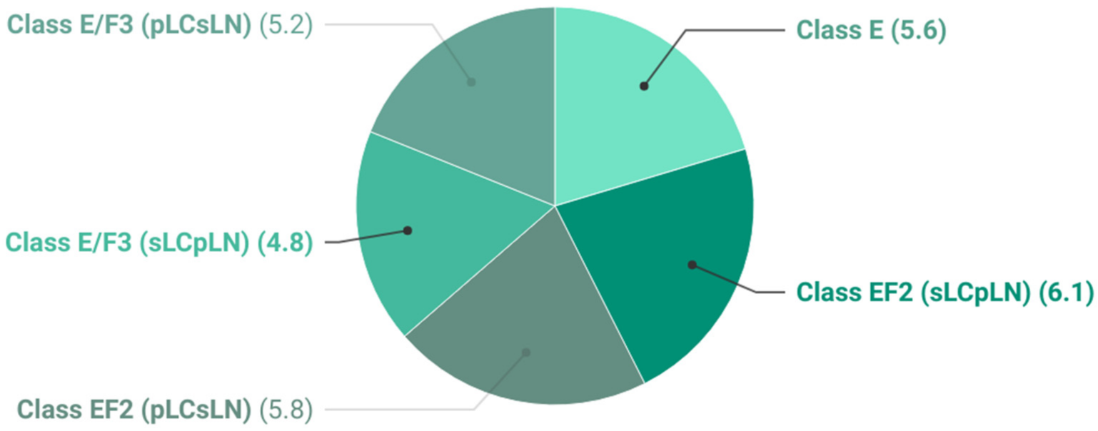
Table 5 demonstrates a comparative cost difference of the class E and enhanced class E inverters. As low power inverters, the components are small in size. Hence, the induced cost for a single inverter is low. However, in general, the cost of building enhanced class E inverters could be more than 20% than that of the class E inverter. In addition, the cost would increase nonlinearly with the power rating of the inverter.
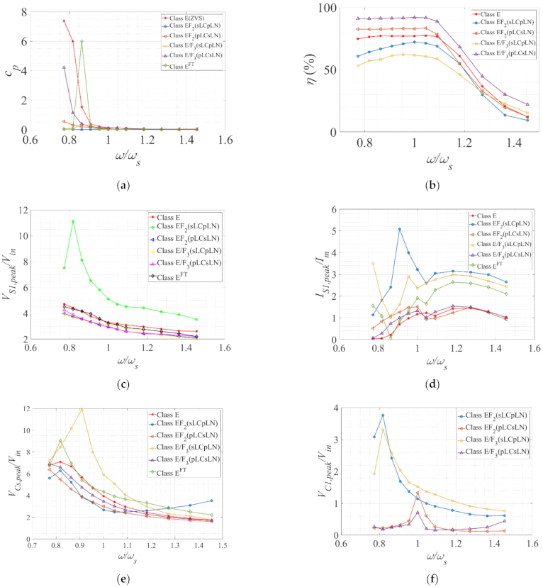
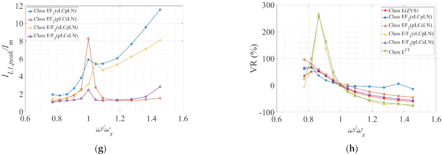
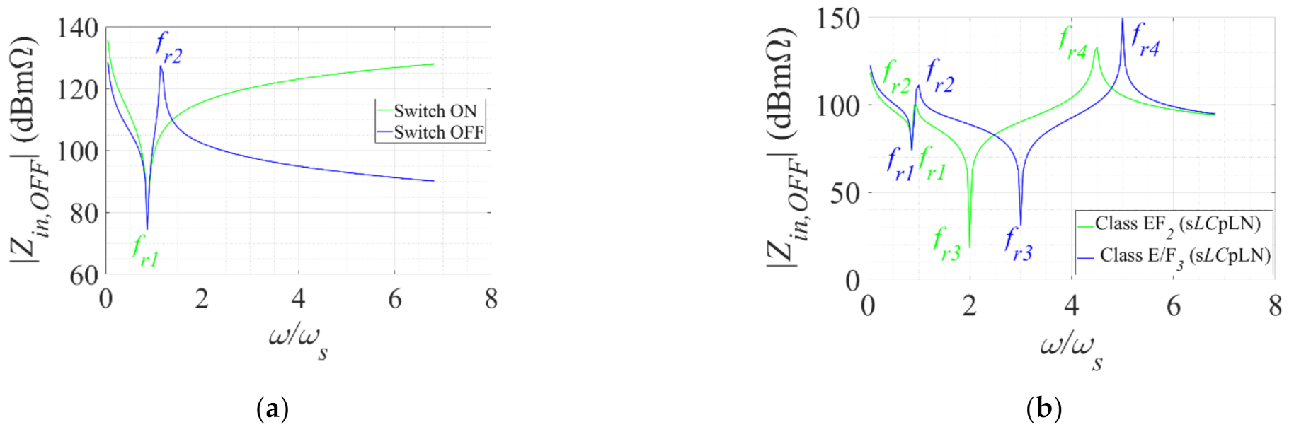
The resonant tank of the inverters is designed to resonate at
fr with a predefined quality factor
Q. By varying the switching frequency
f, the inverter rms output voltage, output power, peak switch voltage and current, and peak voltage across the resonant capacitors are measured. It was observed that the optimum operability (i.e., ZVS) sustained at the vicinity or close proximity of the resonant frequency
fr. The power output capability was maximum in this region. As
f increased, the resonant tank, which behaves like a bandpass filter, blocked the higher harmonics. Resultantly, the power flow was curtailed. Because of the higher input impedance (
Zin), the efficiency also dropped. In general, the peak switch voltage (
VS1,peak) and the peak resonant capacitor voltage (
VC1,peak) dropped with increasing frequency. This is due to the capacitor current (
iCin), which also reduces with increasing
f. The lowest
VC1,peak were recorded for the p
LCsLN configurations for
k < 1. However, as more current was being diverted through the switch (S
1) from the auxiliary networks, there was an apparent rise in the peak switch current (
IS1,peak) for s
LCpLN configurations. These results are demonstrated in
Figure 7a–h.
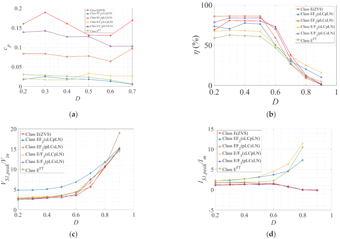
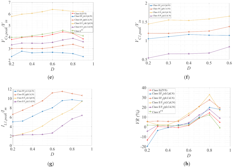
The optimum duty ratio (
Dopt) of class E inverter was 0.50, while for class EF
n and E/F
n inverters, it was approximately 0.40. Any deviation from these values would incur higher switching losses in the respective inverter type due to the loss of soft switching operation. In
Figure 8a–h, the inverters were evaluated by varying the duty ratio (
D) while operating at the corresponding optimum load (
RL,opt) and
fs. It was observed that at extreme
D (≥0.7), the energy delivered to the resonant tank deteriorated due to longer switch ON time. The energy stored in the input inductor (
Lf) increased with
D but mostly diverted through the switch S
1. Hence, the switch voltage and current increases gave rise to switch conduction losses. Subsequently, the efficiency, while remaining fairly constant, dropped at extreme
D. The highest efficiency was recorded for class E and the p
LCsLN configurations at around 80–90% in the proximity of
Dopt. The peak resonant capacitor voltages were relatively unaffected by
D. The peak switch current (
IS1,peak) was significantly higher (2–3 times) for s
LCpLN configurations at
k < 1. However, this could be lowered significantly by operating the inverters at higher
k (>1). This fact is demonstrated in
Figure 8c. The peak auxiliary resonant current (
IL1,peak) in the s
LCpLN configurations became significantly higher at extreme
D however, this could be avoided by increasing
k.
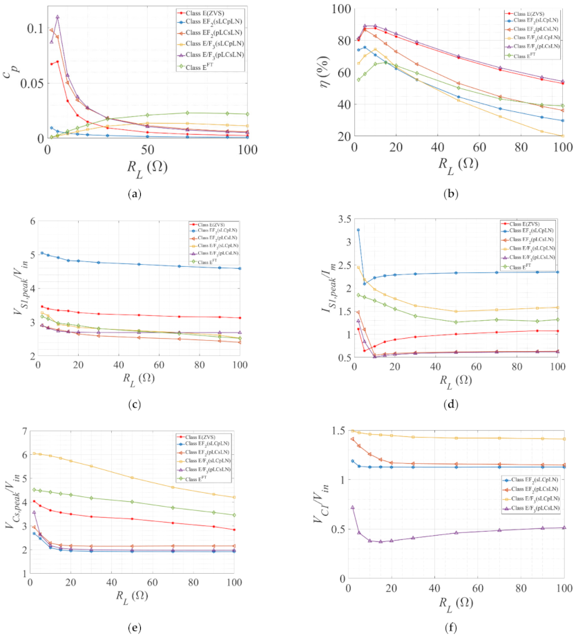
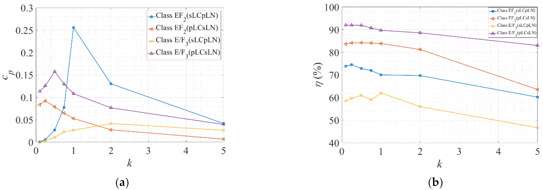
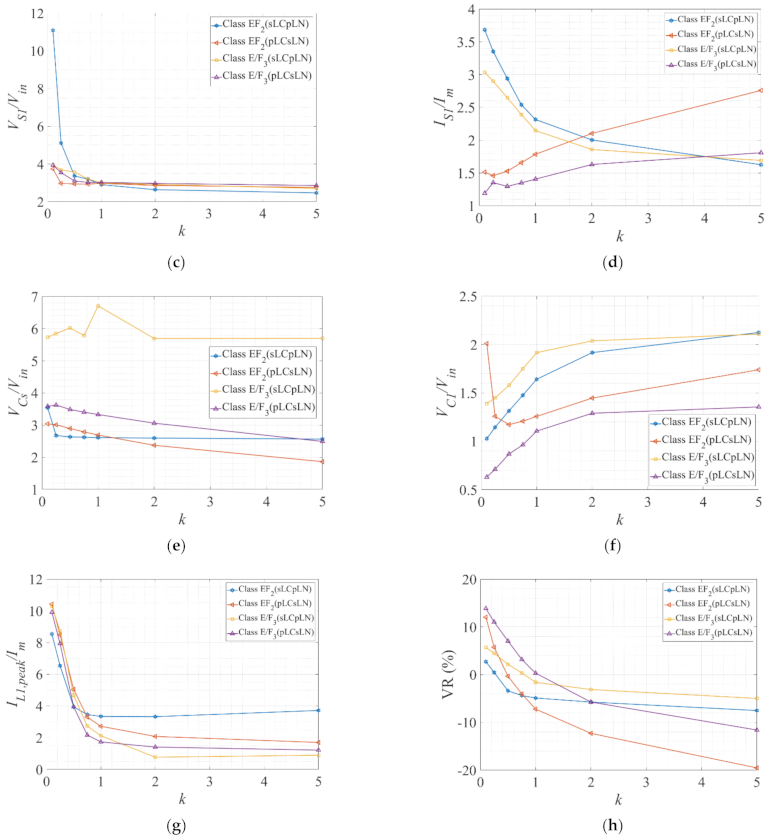
The ratio
k is defined by the ratio of the input capacitance to the auxiliary resonant capacitance (
Cin/
C1). The variation
k can be translated as the variation of the auxiliary resonant components (
L1 and
C1) while keeping
n constant. Hence, by definition, increasing
k means decreasing
C1 and increasing
L1 and vice versa. In general, with increasing
k, the rms output voltage and power output capability (
cp) drops. The efficiency (
η) also drops with higher
k. This is shown in
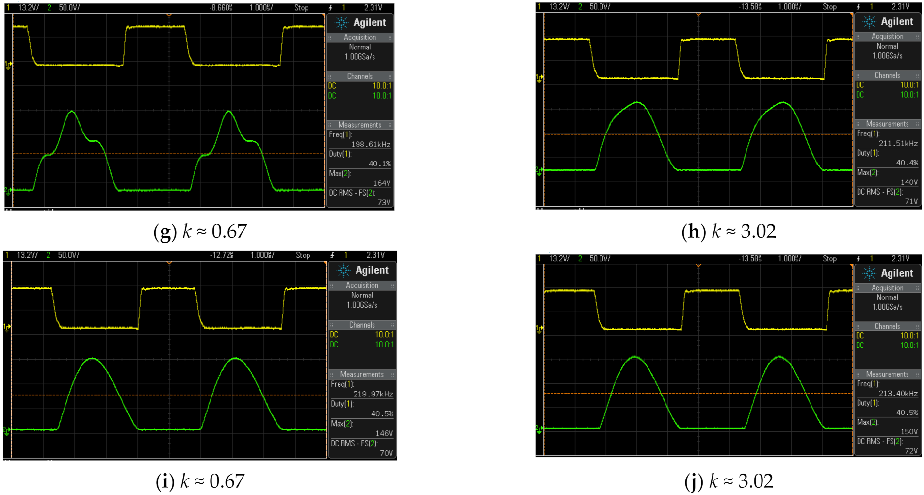
Figure 9a–h.
k < 1,
VS1,peak, and
IS1,peak for s
LCpLN configurations were significantly higher (2–3 times) than class E and p
LCsLN configurations, as mentioned earlier. This was mainly due to the excessive energy that was stored in the large resonant capacitor
C1 and subsequently dissipated through the switch at the turn ON instant. As
k increased, the resonant inductance
L1 became bigger and diverted almost a constant current through S
1. Hence,
VS1,peak and
IS1,peak remained fairly constant at higher
k. However, because of smaller
C1 at higher
k, a relatively larger voltage was induced across
C1 (i.e.,
VC1,peak).
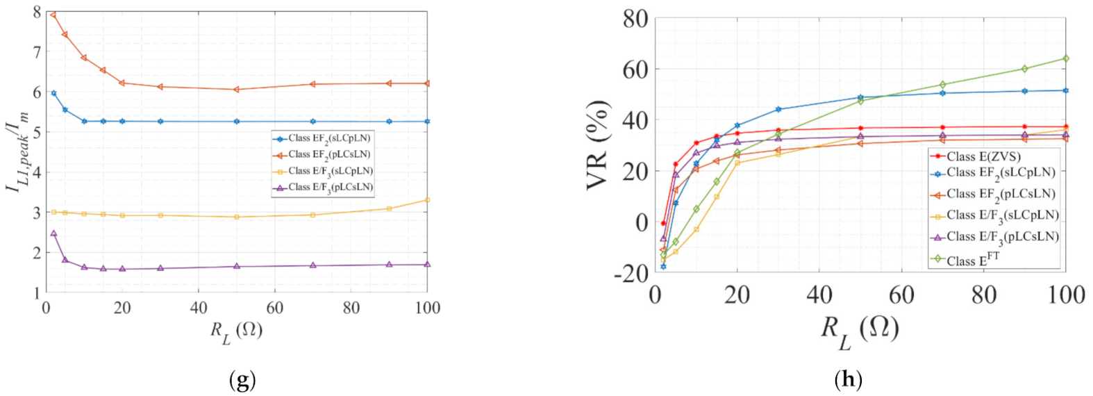
On the other hand, the increasing load resistance (
RL) drove the inverter operating from continuous conduction mode (CCM) to the discontinuous conduction mode (DCM). Hence,
Vout,rms and
cp decreased, with increasing
RL being maximum at
RL,opt. The peak switch voltage and current (
VS1,peak and
IS1,peak) remained fairly constant over the entire load range.
VC1,peak and
IL1,peak were relatively higher (2–4 times) for s
LCpLN configurations. The voltage regulation (VR) was higher at lower loads. The results are demonstrated in
Figure 10.
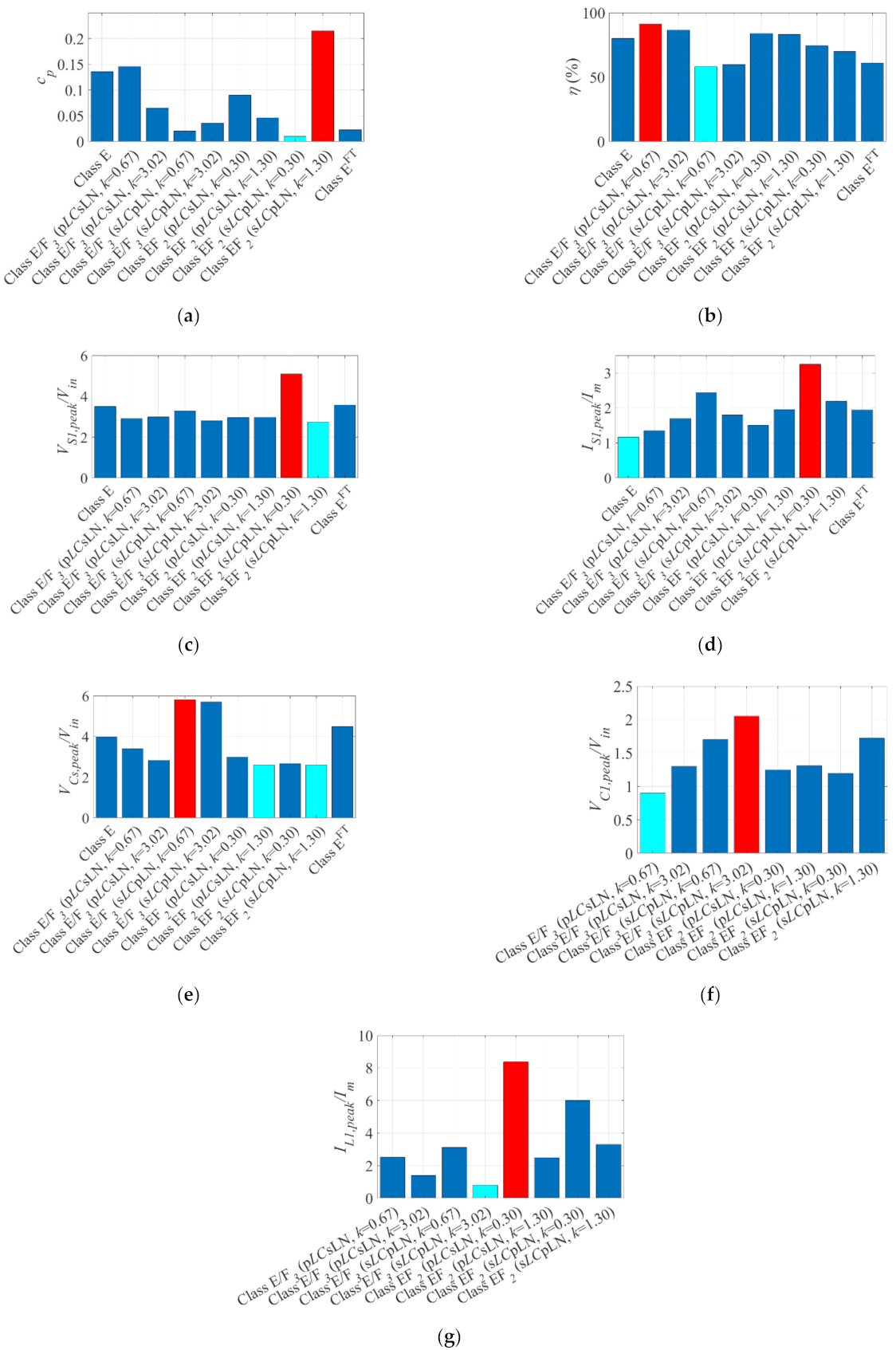
In
Figure 6, the performance parameters recorded at the optimum operating point (
Dopt = 0.50 or 0.40,
RL =
RL,opt) are demonstrated. The maximum and minimum quantities are marked in ‘red’ and ‘sky blue’, respectively. As obvious from
Figure 6a,
cp is maximum for class E and EF
2 (s
LCsLN) configuration at
k > 1, recorded as 0.1356 and 0.215, respectively. The lowest is 0.01 for EF
2 (s
LCsLN) configuration at
k < 1. Again, as shown in
Figure 6b, the class E and p
LCsLN configurations demonstrated higher efficiency compared to the s
LCpLNs. The maximum and minimum efficiency were recorded for class E/F
3 (p
LCsLN) (
k < 1) and E/F
3 (s
LCpLN) (
k < 1) as 91% and 58%, respectively. However,
η did not vary largely with
k. The peak switch voltage in
Figure 6c was generally lower for higher
k. The maximum and minimum are recorded for class EF
2 (s
LCpLN) at 5.1 and 2.74 for
k < 1 and
k > 1, respectively. However, a further reduction of
VS1,peak was possible by increasing
k, as demonstrated in
Figure 9c. The peak switch current (
IS1,peak) was generally higher in s
LCp
LN compared to the pLCsLN configurations. The highest and lowest
IS1,peak were recorded at 3.25 and 1.17 for class EF
2 (s
LCpLN) (
k < 1) and class E, respectively, as demonstrated in
Figure 6d. From
Figure 9d, it can be deduced that selecting
k > 1 and k < 1 for s
LCpLN and p
LCs
LN can minimize
IS1,peak further. The peak voltage across the resonant capacitor (
VC1,peak) was lower for p
LCsLN configurations (2–3 times than s
LCp
LN in general), as can be observed in
Figure 6f. This is expected as the voltage across the load network is shared across the capacitors Cs and C1 for p
LCs
LN configurations. On the other hand, the peak current in the auxiliary resonant network (
IL1,peak) is notably higher for
k < 1 (See
Figure 9g). The summary of these findings and optimum operating conditions for enhanced inverters are accumulated in
Table 6.
In addition to the comparison presented in
Figure 7,
Figure 8,
Figure 9 and
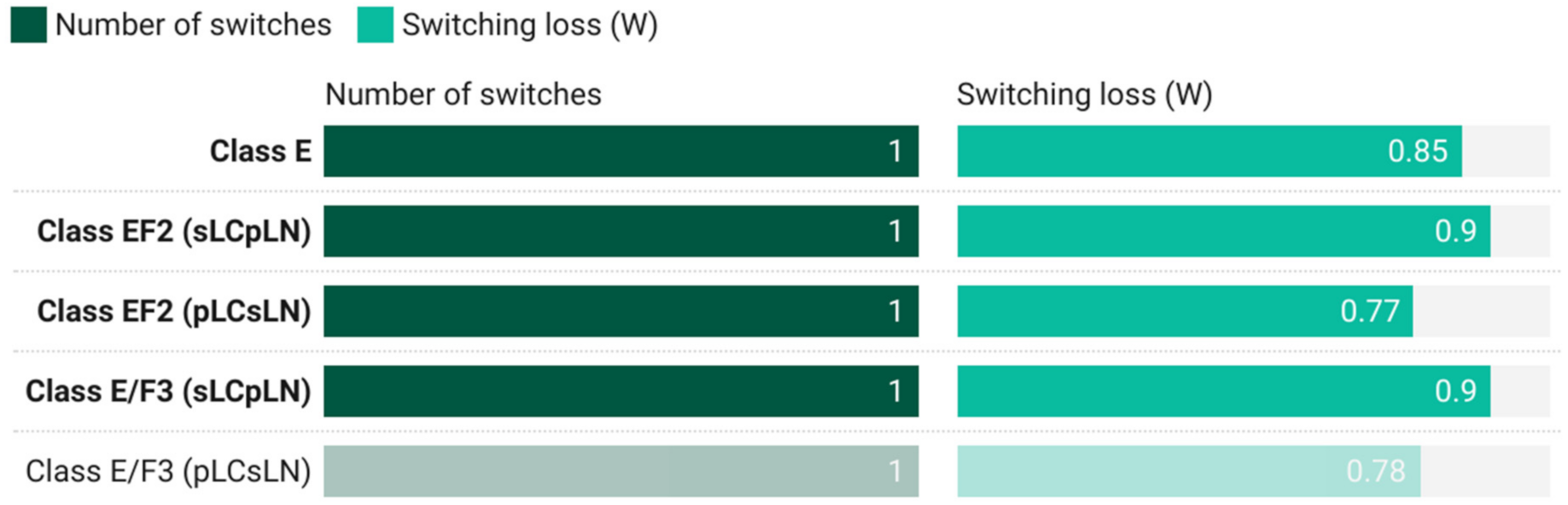
Figure 10, the switching losses and THD are demonstrated in
Figure 11 and
Figure 12 respectively. As can be observed, the switching loss is minimized due to application of ZVS and ZVDS. The percentage loss is maximum for class EF
2 (s
LCp
LN) at approximately 3.6%. The loss is minimum for class E/F
3 (p
LCs
LN) inverters at 3.08%. The THD can be greatly improved by adding extra filter at the output of the inverter.


 ,
, 


