1. Introduction
Electromagnetic interference (EMI) can be defined as signals that unintentionally disturb an electrical or electronic system’s regular operation. These disturbances can affect the electrical or magnetic magnitudes of its circuits [
1,
2,
3]. Thereby, the problem of interferences is an issue that design engineers continually faces [
4] since EMI can cause different kinds of problems in digital and analog systems, leading to malfunctions, system reboots, or even permanent damage to the system if it is not properly designed or protected [
5]. The security of an electronic system where there are devices that produce electromagnetic disturbances and elements or small-signal circuits, sensitive to such disturbances, depends on the compatibility of the signal levels used. Hence, it is convenient to comply with specific design rules that make the disturbance levels generated by the interferences source elements compatible with the signal levels used by the possible victim elements or elements sensitive to such interferences [
6,
7,
8,
9].
The continuous implementation of new advanced functionalities and the miniaturization of electronic devices for embedded systems has become a serious difficulty in terms of electromagnetic compatibility (EMC), especially in those than integrates communication modules [
10,
11,
12]. This evolution usually involves a higher component integration, printed circuit board (PCB) size and thickness reduction, and the miniaturization of the device housing [
13,
14]. These design principles are often used to achieve a device with better performance and features; however, they increase the likelihood of generating complex EMI problems [
15,
16,
17,
18,
19,
20].
Some standards establish the maximum limits of interferences to ensure that the equipment is compatible and does not interfere. Thus, EMC is the ability of a system to operate satisfactorily in its electromagnetic environment without introducing disturbances above the normalized limits in that environment and withstanding those produced by other equipment. In order to comply with these regulations applied to electronic equipment, it is necessary to carry out measurements to certify that this equipment complies with regulations. Detection and correct characterization of the EMI is an important factor in designing a suitable solution. Thus, it is essential to perform EMI measurements using different instrumentation, measuring probes and antennas to detect the electromagnetic fields that can provide information to the designer from undesired signals [
7].
Compliance measurements performed according to the different EMC regulations are generally carried out using expensive and complex test equipment and facilities. However, pre-compliance EMC measurements can be performed previously in the product development laboratory, with equipment that can provide good indication of the EMC performance of a product, using a near-field antenna and a spectrum analyzer. Although the results obtained by these “in-house” measurements are not as accurate as compliance EMC measurements, performed in a test facility with normalized and controlled environment, they are simple, quick, and easy to perform. In doing this, we achieve a good balance between cost, speed, and accuracy in the prototype design [
21]. This is especially important at the first stages of the design process but is also interesting in troubleshooting or debugging tasks, when the device under test fails the standard tests [
22,
23]. Data from EMC test laboratories indicate that 85% of the products submitted for final compliance testing fail the first time [
24]. Thereby, it is strongly suggested to designers, to carry out pre-compliance measurements or improve the design stage in order to achieve better results for compliance. The advantages of early pretest—EMC testing during the design stage of a product include the following [
24]:
Therefore, EMC considerations should be part of the design process, to improve early detection and reduction of such interference, a part of the design stage to comply with the regulation, essential to save the cost of the overall product [
16,
25]. Obviously, the most critical radiating sources are currents flowing around loops on a PCB since they can result in differential-mode radiation. These undesired and unintended current loops act as small-loop magnetic antennas. Depending on the inductive parasitic parameters, the radiation can result in strong near-field and far-field emissions. Radiated emissions are measured in far-field following the compliance testing. They are regulated by standards to verify our system does not interfere with other equipment [
26]. Nevertheless, radiated emissions in the nearfield are not always detected by standard tests, but they might affect other parts of the same PCB or other systems located near the radiating source. The far-field procedures are based on measuring the radiated fields with a broadband horn antenna or patch antenna located at far-field distance from the device under test (DUT) to identify the field’s source and strength [
19,
27,
28,
29]. Since the probe antenna size is large, it is generally not possible to efficiently measure the fields from a small source. The magnetic near-field probe (NFP) represents a more suitable tool to measure the field levels from a small source [
16,
30]. It is important to gain insight into the physics underlying current sources and NFPs are effective diagnostic tools for providing that expertise [
31]. A magnetic NFP antenna is a loop antenna that is shielded in order to selectively measure the magnetic field (
H-field) whereas the electric field (
E-field) is shielded [
16,
32]. Thereby, a shielded magnetic field probe will detect paths of high currents (di/dt) but not high voltage points (dv/dt) [
24,
26]. This kind of antenna is useful as a magnetic field probe for emission pre-compliance measurements or debugging tasks since the user can scan the PCB looking for locations with strong magnetic fields [
31,
33]. When a strong magnetic emission area is found, the designer should check the PCB layout and components placement in that area to locate the current sources [
22,
34,
35]. Subsequently, the designer can modify the PCB or introducing filters or board-level-shielding (BLS) solutions to reduce the emissions and retest it to confirm that the amplitude of the fields has been decreased [
19,
22]. Perhaps the problematic area found on the PCB is not translated into not passing the far-field compliance test, but this source of radiation could be coupled to other larger paths such as cables. Cables usually can be turned into a more effective antenna, producing radiated emissions in the far-field measurement [
24,
26].
This contribution focuses on analyzing the performance of an antenna easy to build, low-cost,
H-field NFP that has been designed and manufactured using a standard PCB stack-up, as shown in
Figure 1. Design has been made using Finite Element Method (FEM) simulations. Thereby, the frequency range and sensitivity of the NFP-PCB is analyzed through a FEM simulation model that makes it possible to evaluate its sensibility and effective frequency range. Thereby, the aim of this contribution is to show a new
H-field NFP design, not a new modeling technique, since FEM modeling will allow us to develop small modifications in the NFP design in order to improve its behavior in the future designs. The results obtained from the simulation are validated by means of an experimental measurement setup. The accuracy of the study is corroborated though comparing scattering parameters provided by the FEM simulation model and experimentally through vector network analyzer equipment. The NFP-PCB is compared to two high-quality commercial probes in order to analyze its performance. Finally, the sensitivity of the NFP-PCB to electromagnetic field is analyzed by means of the simulated near-field distribution, and the far-field is measured to determine the radiation pattern levels normalized in dB.
This manuscript is organized as follows.
Section 2 describes the design parameters and the main features of the designed and manufactured NFP-PCB. The measurement and calibration setup and the details of the FEM simulation model are covered in
Section 3 and
Section 4, respectively. Subsequently,
Section 5 analyses and discusses the performance of the NFP-PCB in terms of the scattering parameters and spatial magnetic field distribution; bandwidth and sensitivity were also evaluated. In
Section 6, the designed NFP-PCB is compared to two high-quality commercial antennas. The performance of the NFP-PCB is characterized in terms of far-field by determining the radiation pattern levels. Finally, the main conclusions of the research are summarized in
Section 8.
2. Near-Field Probe Design
Our NFP probe is a small loop antenna sensitive to the magnetic field. The measurement mechanism of a magnetic NFP is based on the principle of Faraday’s law since the induced current is related to variation of the magnetic flux in its enclosed surface. Thereby, it could be possible to manufacture any magnetic NFP from a basic loop (
Figure 2a) and approaching a relationship between the output voltage (
Vm) provided by the probe and the component of the incident
H-field that is perpendicular to the loop’s area [
22]:
In (1), it is assumed that the loop antenna is composed of
n wire turns enclosing the area
A, ω the angular frequency,
B the incident magnetic field, and θ the angle between the magnetic field and a perpendicular to the plane of the loop. However, this kind of antenna is sensitive to both electric and magnetic fields, making it less effective diagnostic tools than more sophisticated probes designed specifically for electric or magnetic fields [
24].
From Equation (1) it is possible to determine that the NFP design is a trade-off between sensitivity and spatial accuracy because both are associated with the size of the probe [
36]. The smaller the probe, the more accurately it can locate signals, but the less sensitive it will be [
26,
37]. Consequently, the size of the probe loop is inversely proportional to its spatial resolution [
38]. Thereby, it is more interesting to design NFP with small
A because the sensitivity or probe gain parameter can be increased by introducing a preamplifier module between the own NFP and the measuring equipment. In Equation (1), it is also evident that NFP position relative to the PCB under test provides maximum signal when the NFP vector surface is parallel to the field and minimum when orthogonal. Thus, when analyzing near-fields, the NFP should be moved and rotated gently to pick up the current sources. Another parameter extremely important is the distance from the NFP antenna to the current sources since the magnitude of the field strength falls off as the cube of the distance from the currents [
22]. Therefore, with these assumptions it is possible to estimate the response of the NFP in terms of output voltage versus magnetic field.
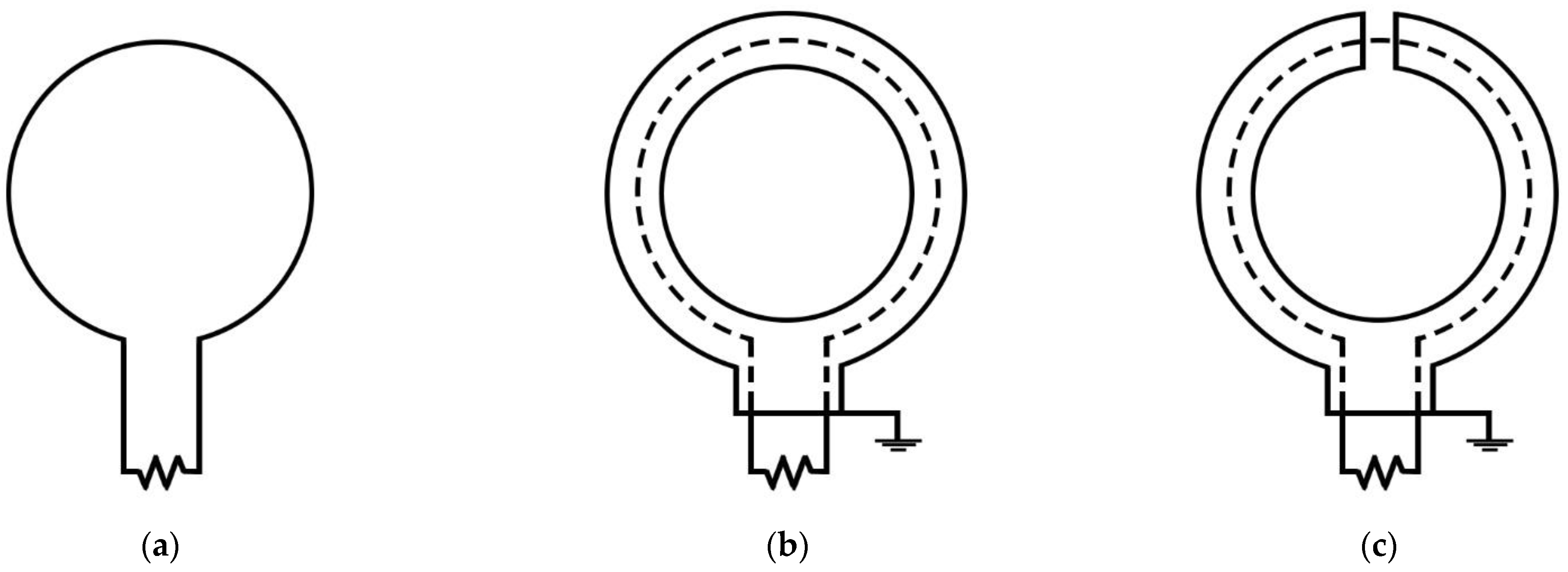
A well-designed magnetic field probe based on a loop should be shielded with an external conductor covering the loop, as shown in
Figure 2b, to shield the loop from the electric field and make measurements insensitive to it [
16]. Nevertheless, this configuration allows some current flow through the shield, which has some influence in the measurement. A widely used technique to prevent these currents is based on splitting the shield to provide and open circuit in the shield. Thereby, this procedure can be implemented by cutting the shield at the top, as shown in
Figure 2c, in order to minimize currents in the shield and increase the sensitivity to
H-field against the
E-field [
22].
It is very important to introduce the gap that splits the shield symmetrically, in the center of the top side of the loop, to keep a balanced and symmetrical structure. A better shielding effectiveness is achieved if the gap is located in the middle of the loop as shown in
Figure 2c. A non-symmetrical shielded loop would not cancel out the flowing currents associated to tangential
E-field and would be sensitive to this tangential
E-field. These un-balanced currents would induce a secondary magnetic field which would induce secondary extra signal in the central conductor, masking the first one associated to the intended
H-field measurement [
23,
34]. When this narrow aperture on the shielding layers is located at the middle of the loop, and then the common-mode currents on the external surface of the shield from the
E-field can be cancelled based on the symmetric distribution, the NFP is placed perpendicular to the source of emissions [
39]. Moreover, the small gap of the shield opening is also introduced to enhance the sensitivity of the magnetic probe, and it defines the spatial resolution to pinpoint the interference sources [
16,
39]. The gap introduced in the designed NFP-PCB antenna presented in this contribution has been selected according to the recommendation proposed in the IEC 62333-2 standard intended to specify the methods for measuring electromagnetic characteristics of BLS solutions [
40]. This standard recommends designing a shielded multi-layered probe with a gap (slit) delimited with the following relation in order to obtain a balance between high-spatial resolution and sensitivity:
where
Фa is the average diameter of the loop probe.
Different techniques can be used to design a magnetic NFP depending on the desired sensitivity, frequency range, or spatial resolution. Thereby, in [
41], it is proposed a rectangular magnetic field probe tested in the 1–7 GHz region that provides sensitivity in terms of S
21 parameter of −40 dB at 1 GHz, achieving up to −25 dB at 7 GHz. This is an interesting design that is implemented into a PCB, but its geometry and dimensions are not intended for debugging tasks since the user cannot easily scan a completed PCB. In [
42], it is described a miniatured
H-field probe for near-field measurements in the 9 kHz–20 GHz frequency region, but it does not provide a flat response in the whole range. The NFP characterized in [
39] is manufactured in low-temperature co-fired ceramics and shows a good performance of spatial resolution, working frequency band (up to 20 GHz, providing a flat response in the high-frequency region), and electric field suppression, but it is very complex, and it is not manufactured in a PCB. On the other hand, the NFPs presented in [
43,
44] proposed a probe fabricated using a four-layer stack-up PCB with a geometry that allows the user to carry debugging tasks with a handheld tool. The performance of the NFP described in [
43] is limited from 1 MHz up to 1 GHz, and it is not provided the sensitivity parameter in terms of the S
21 parameter, whereas the NFP characterized in [
44] offer a flat response with an average sensitivity close to −40 dB in the 1–2 GHz region. Thereby, the NFP proposed in the contribution is designed to be manufactured in a PCB with a geometry and dimensions that allow the user to detect near
H-field emissions within a device or PCB design. This NFP should provide a flat response in terms of sensitivity, covering a frequency region similar to commercial high-quality near-field probes [
45].
The proposed shielded
H-field NFP is made of six layers PCB of FR-4 TG140. The layer sack-up is overlaid as shown in
Table 1. The copper thickness for all layers is 35 µm, the cores are 300 µm thick, and the prepreg material type 2116 is 115 µm. The dielectric constant
εr of the PCB used is 4.4 and the final thickness is 1.55 mm after the pressing procedure. Actually, the design could be implemented in a four-layer stack-up in terms of electrical operation, but two extra-layers have been added with the aim of improving the insulation of the PCB against the hazard of electric shock. In a four-layer PCB, the Top and Bottom layers are covered by two metal planes, and the tracks are routed in the two inner layers. This structure can be dangerous if the silkscreen layer that covers both Bottom and Top layers are damaged and, thus, exposing it. If these are non-insulated and the metal planes accidentally touch electrical circuits or components the own DUT, the measurement equipment or the user could be damaged [
24]. Thereby, the NFP designed is based on a six-layer stack-up with the following structure:
Top and Bottom layers are intended to insulate the NFP-PCB and provide the pads to connect the SMA connector that provides the output signal.
Inner layers 1 and 4 represent the shielding layers against E-field. The whole area is covered by a copper plane (except in the gap area).
Inner layers 2 and 3 contain the symmetrical tracks that make up the loop and the transmission line that interconnects it with the SMA connector.
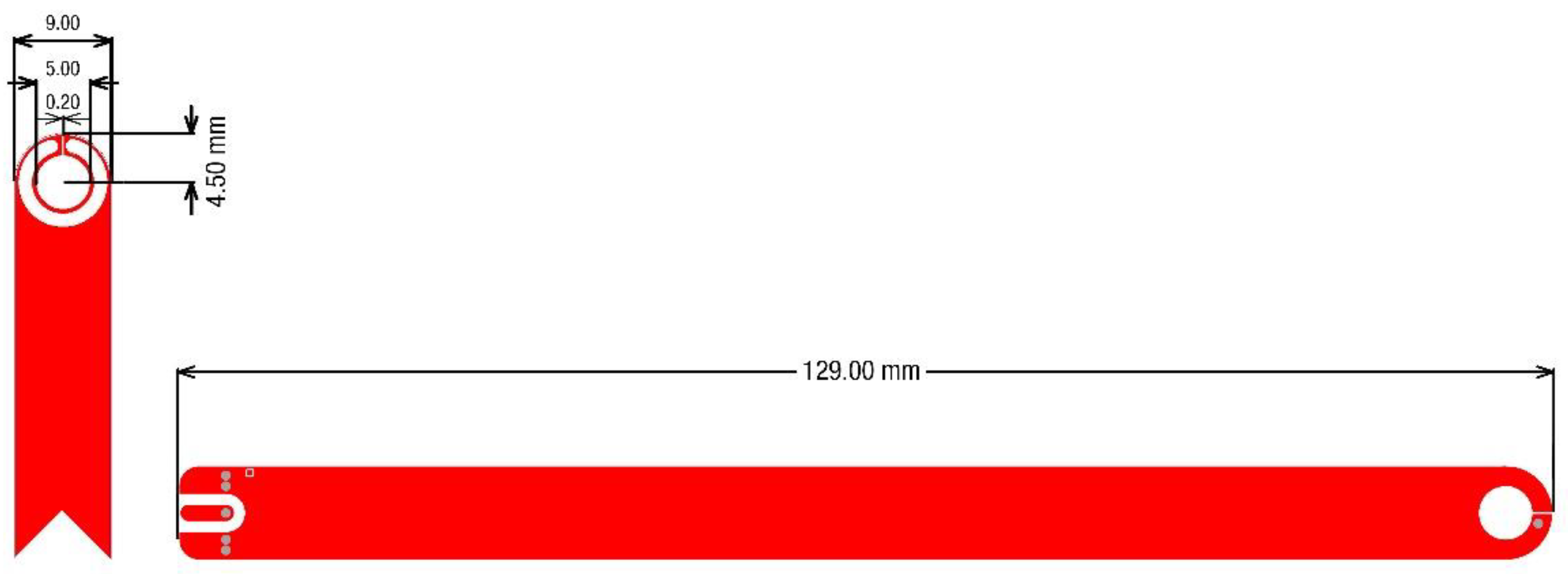
The proposed NFP-PCB consists of a half-turn track that conforms a returning path to the two shielding ground planes with a short circuit via. As explained above, these two ground planes have a small opening that is used for the field coupling. The gap introduced is 0.2 mm, whereas the diameter of the loop is 3.2 mm. These dimensions agree with the design requirements defined by the standard [
40]. The half-turn track is connected with the output SMA connector through a 50 Ω strip line, according to the input impedance of most RF-measuring instruments, in order to prevent resonances in the track. Thereby, undesired resonances are prevented. The total dimensions of the NFP-PCB without SMA connector are 9.0 mm width and 129.0 mm length, as shown in
Figure 3. The width was selected attending the SMA dimensions with the aim of improving NFP-PCB robustness.
3. Measuring Setup
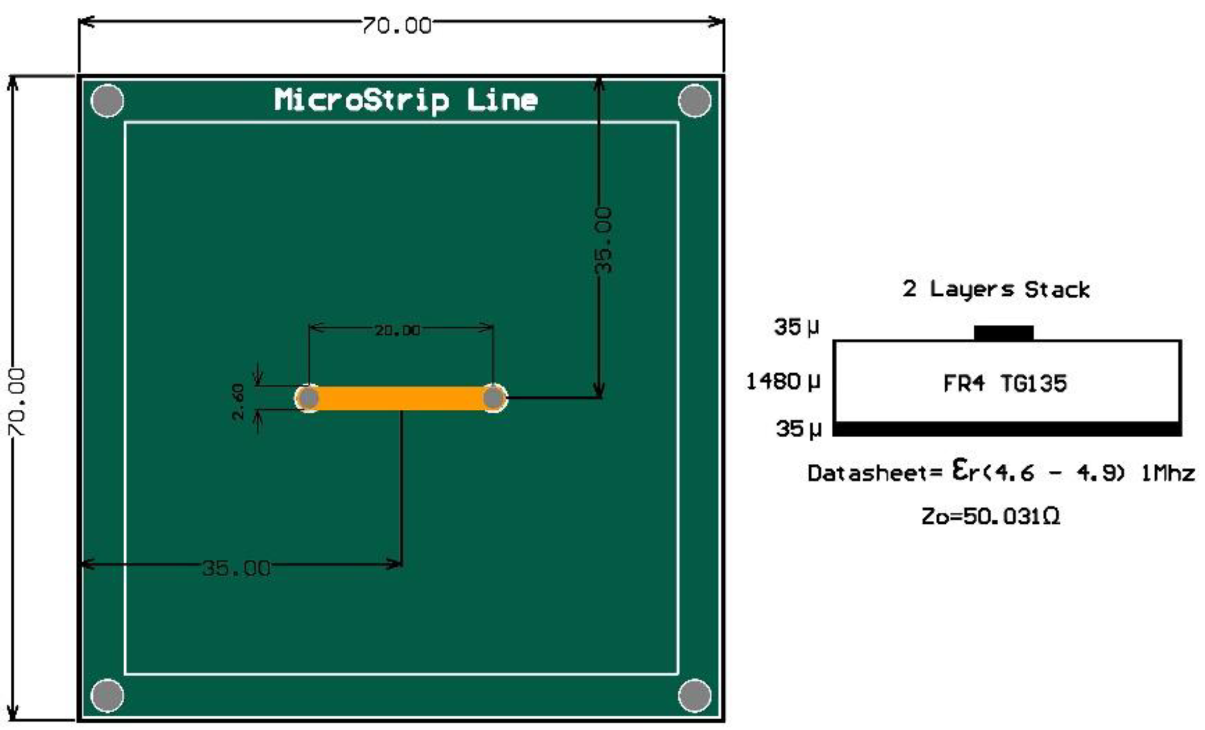
The NFP-PCB performance is analyzed by means of the scattering parameters or S parameters and also by a careful analysis of the near-field spatial distribution. Thereby, the NFP-PCB is characterized in terms of its response, bandwidth, and sensitivity. The measurement setup designed to evaluate the performance of the NFP-PCB uses a 50 Ω microstrip line (MSL) as a radiating source. The MSL is implemented in a FR-4 TG135 substrate PCB with dimensions of 70.0 mm length, 70.0 mm width, and 1.55 mm thickness, as shown in
Figure 4. It consists of a two layers PCB, where, on the top side, the copper strip conductor with 20.0 mm length, 2.6 mm width, and 0.035 mm thickness is printed. On the bottom side, a ground plane of copper with 0.035 mm thickness is placed, and two SMA connectors are connected one at each end of the strip conductor. The SMA connectors are placed on the Bottom layer, and they were connected with both ends of the MSL through two vias.
This MSL fixture is powered by a sweep frequency signal with a fixed power that generates a specific field that is acquired by the NFP by means of the S parameters. This measurement setup was numerically modeled with a FEM simulator to determine the S21 of the NFP-PCB in order to make comparison with the experimental measurements obtained from the experimental setup. The FEM simulation also provides the spatial distribution of the magnetic field strength.
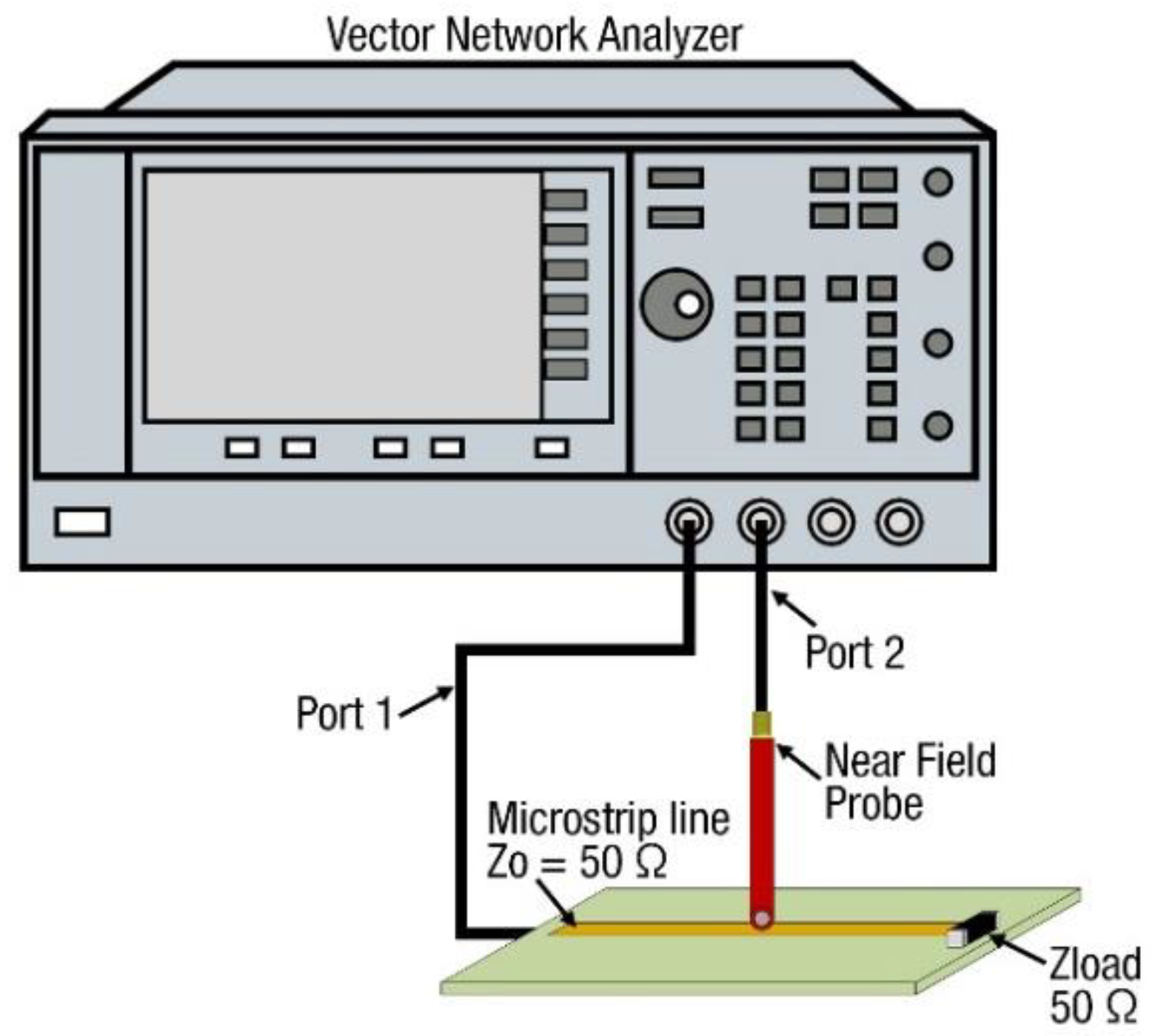
The NFP is analyzed in terms of the S
21 parameter obtained with the MSL following the scheme of
Figure 5. In the experimental setup, the NFP probe is located next to the MSL connected to the vector network analyzer (VNA) [
46,
47]. Thereby, one SMA connector of the MSL is connected to the VNA and the other is ended with a matched 50 Ω load. The MSL acts as a source of radiated electromagnetic field that is measured by the NFP. The NFP is connected to the second port of the VNA and is placed over the center of the strip conductor forming a right angle with it as shown in
Figure 5. Subsequently, the S
21 parameter is evaluated through only measuring the radiated energy by the MSL. The distance was set at zero mm from the strip line to the NFP.
4. FEM Model
The FEM simulation modeling is carried out with the software Ansys HFSS 3D electromagnetic simulation platform (Ansys Electronics Desktop) [
48]. We use the Ansys package with FEM for convenience in performing the modeling. This software allows direct import of the file with the geometry and layout of the circuit from the CAD platform and allows automatic meshing, which saves a lot of work. Ansys, in this way, allows a very fast modeling of the structure. After importing the file with the geometry and dimensions, all that remains is to define the characteristics of the materials and the boundary conditions.
The objective of this work is to present a new measurement probe, with a modeling that allows obtaining fast results under small changes. FEM modeling with Ansys allows making small changes very quickly to improve the probe design in prototypes. Other numerical techniques, such as FDTD, could be used, [
49,
50]; in fact, we could have modified some of our programs for that purpose [
51,
52]. The FEM results can be compared with experimental or from other techniques. The proposed simulation model is shown in
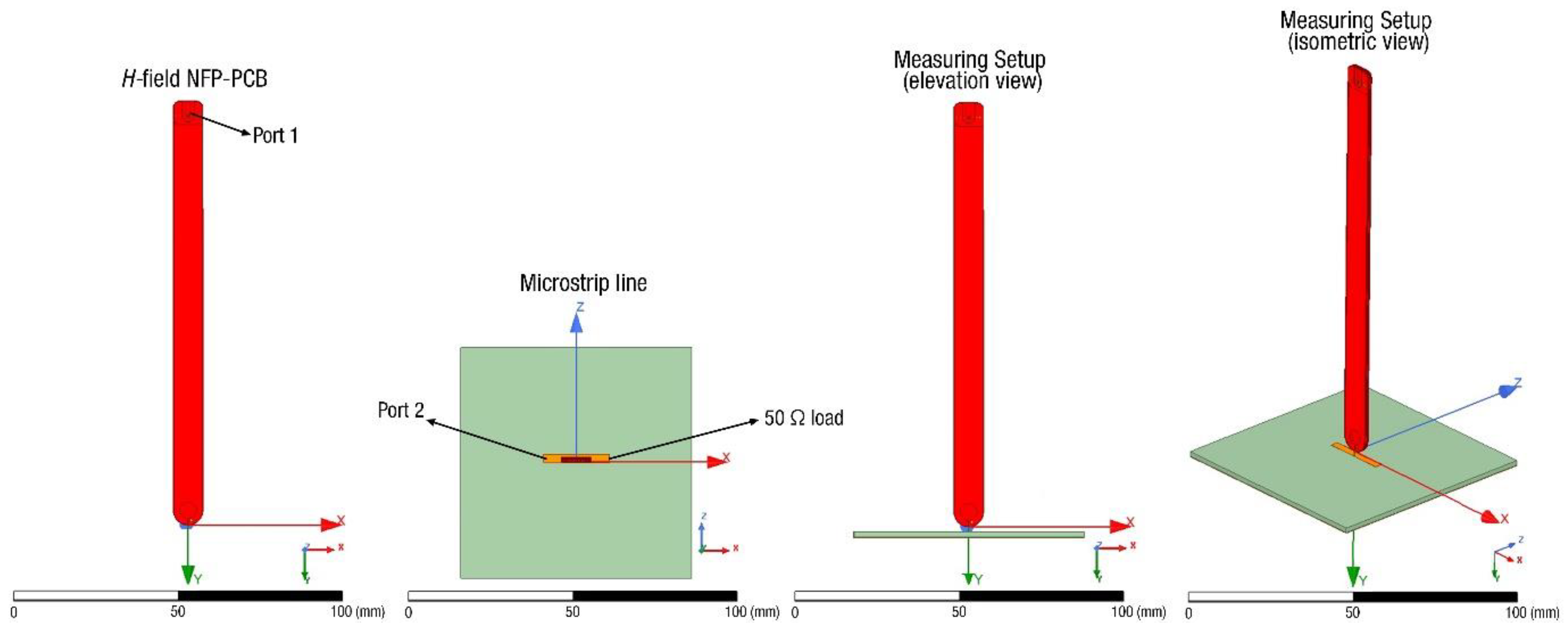
Figure 6. The NFP was placed vertically on top of the MSL with zero distance between them in order to obtain the maximum receiving signal. One of the ends of the strip conductor is connected to a port that provides the frequency sweep signal to the MSL. The other end of the strip conductor is matched with 50 Ω load. A second port is connected to the end of the NFP-PCB in order to obtain the signal acquired by the probe. Thereby, it is possible to emulate the desired measurement setup and obtain the S
21 parameter to be compared with the experimental results to verify the results. The S
21 parameter, or transmission parameter, versus frequency will provide the bandwidth in which the antenna shows a flat response. The reflection coefficient (S
11 parameter) can be obtained by doing a FEM simulation of the NFP-PCB by itself, without the MSL. In this case, only the lumped port connected to the output connector of the probe is considered. Furthermore, spatial
H-field strength distribution in terms of parallel and vertical planes to the NFP-PCB, as well as its total gain is analyzed to obtain the sensitivity parameter.
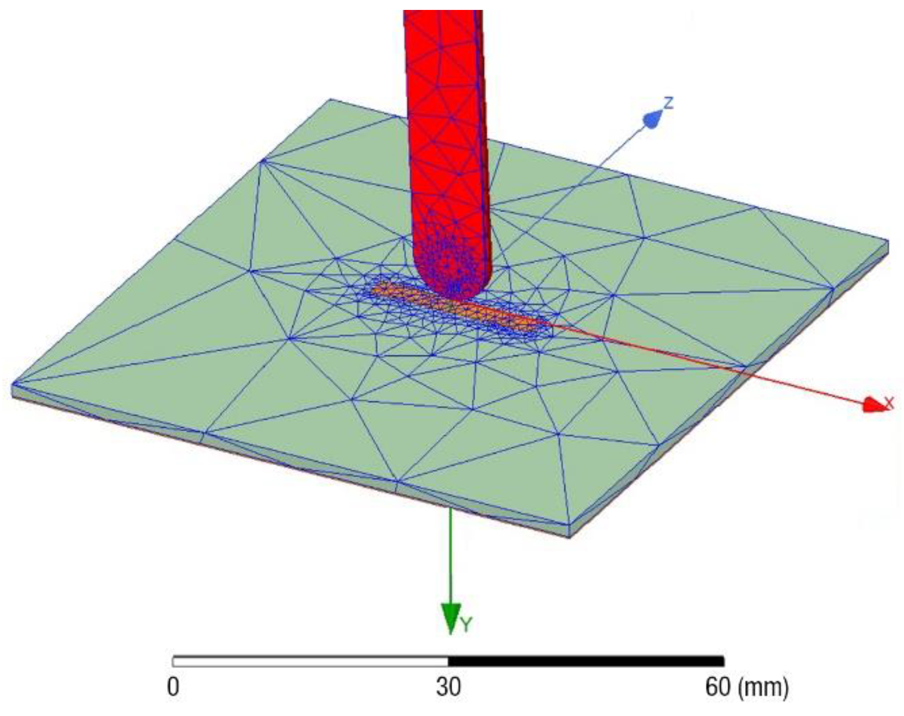
The FEM numerical mesh involves both the MSL described above and the NFP-PCB antenna. The mesh operation has been applying on the radiation boundary that is defined as an airbox separated from the sides of the 3D model a factor of λ/4, considering the maximum operation frequency [
53]. This simulation software applies an automatic adaptive meshing procedure that accurately and efficiently calculates the fields in a model. The process starts with translating the modeled geometry into a conformal, inhomogeneous tetrahedral mesh. This mesh is coarse in areas where the geometry consists of large objects and dense in areas where the geometry has fine features. This initial mesh is refined to limit the maximum size of the mesh elements and comply with any user-specified mesh operations [
54]. The maximum size of the mesh elements has been determined by λ/4, considering the maximum operation frequency [
53]. The first adaptive pass is completed by solving this mesh at the single solution frequency to determine the fields and S parameters of the model. This automatic adaptive process continues until the mesh converges. The mesh is converged when the S parameters change between two consecutive adaptive passes by less than a user-specified convergence criterion. When the mesh adapting process is completed, Ansys HFSS will solve the mesh at numerous frequencies to determine the user requested frequency behavior of the model [
54].
Figure 7 shows the mesh applied to our measuring setup model.
In terms of numerical computing, Ansys HFSS software solves the field vector wave equation [
48]:
where
µr and
εr are the relative permittivity and permeability, respectively,
c is the speed of the light in the vacuum,
ω is the frequency, and
are the source currents.
The magnetic field is obtained using the Maxwell’s curl equation:
E-field is expanded as a linear combination of orthogonal basis functions as follows [
55]:
where the values
xi at each finite element are the unknowns and
N is the number of elements.
Using Green’s and Divergence Theorems with the orthogonal basis functions
, vector wave equation leads to
The above equation has the form:
or
where boundary conditions are in
A-matrix and excitation terms are in
b.
The above equation is solved by
L-U decomposition [
55]:
where
L is a lower triangular matrix and
U is upper triangular matrix [
56].
The above equation is efficiently solved by Ansys through forward-backward substitution [
48]:
Note that Ansys HFFS software has been widely used and optimized for this type of problems for the last thirty years [
57].
5. Numerical Results and Measurements
The numerical results obtained with the FEM models of above section are validated against measurements to verify the design and performance of our NFP. The FEM model reproduces the experimental procedure which is used to evaluate the performance of the NFP. The FEM simulation is a three-dimensional modeling of
Figure 8, with exception of the pigtails and VNA equipment.
Figure 7 shows a photograph of the actual measurement setup, it includes a fixture to hold the MSL and NFP, as well as the E5071B VNA.
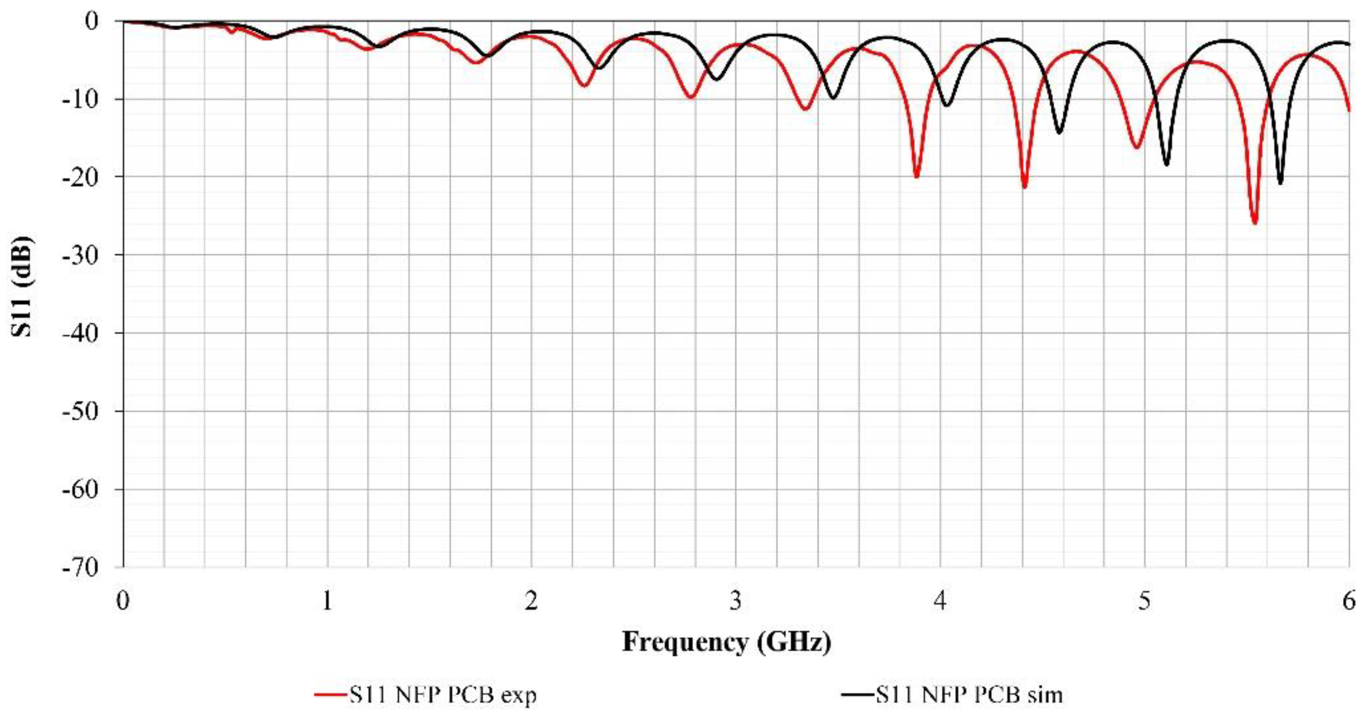
Figure 9 shows the S
11 measurements and FEM numerical data. It is possible to observe a significant mismatch between both numerical and measured values that increases with increasing frequency. It should be noted that the environment around the fixture setup was not modeled, and some parasitic capacitance exists between the MSL the holding structure and the VNA, as well as the desk, this small capacitance is constant and provides this small shift in S
11 with increasing frequency. Better experimental results would have been obtained by measuring inside an anechoic chamber with absorbing panels around the assembly. However, this difference disappears by smoothing both numerical and experimental data.
Table 2 shows a comparison between the S
11 measurements and FEM numerical results. At the top of this table, it is possible observe the relative error for several frequency values and the mean of this. Thereby, a mean relative error of 114.77% is obtained when both traces are compared. This significant error is caused by a parasitic capacitance generated by the surroundings of the experimental measuring setup that is not considered in the simulation model. Nevertheless, if a shift of 550 MHz is applied to the S
11 experimental trace, this mean error is reduced up to 17.60% since the resonance peaks and maximum values are synchronized.
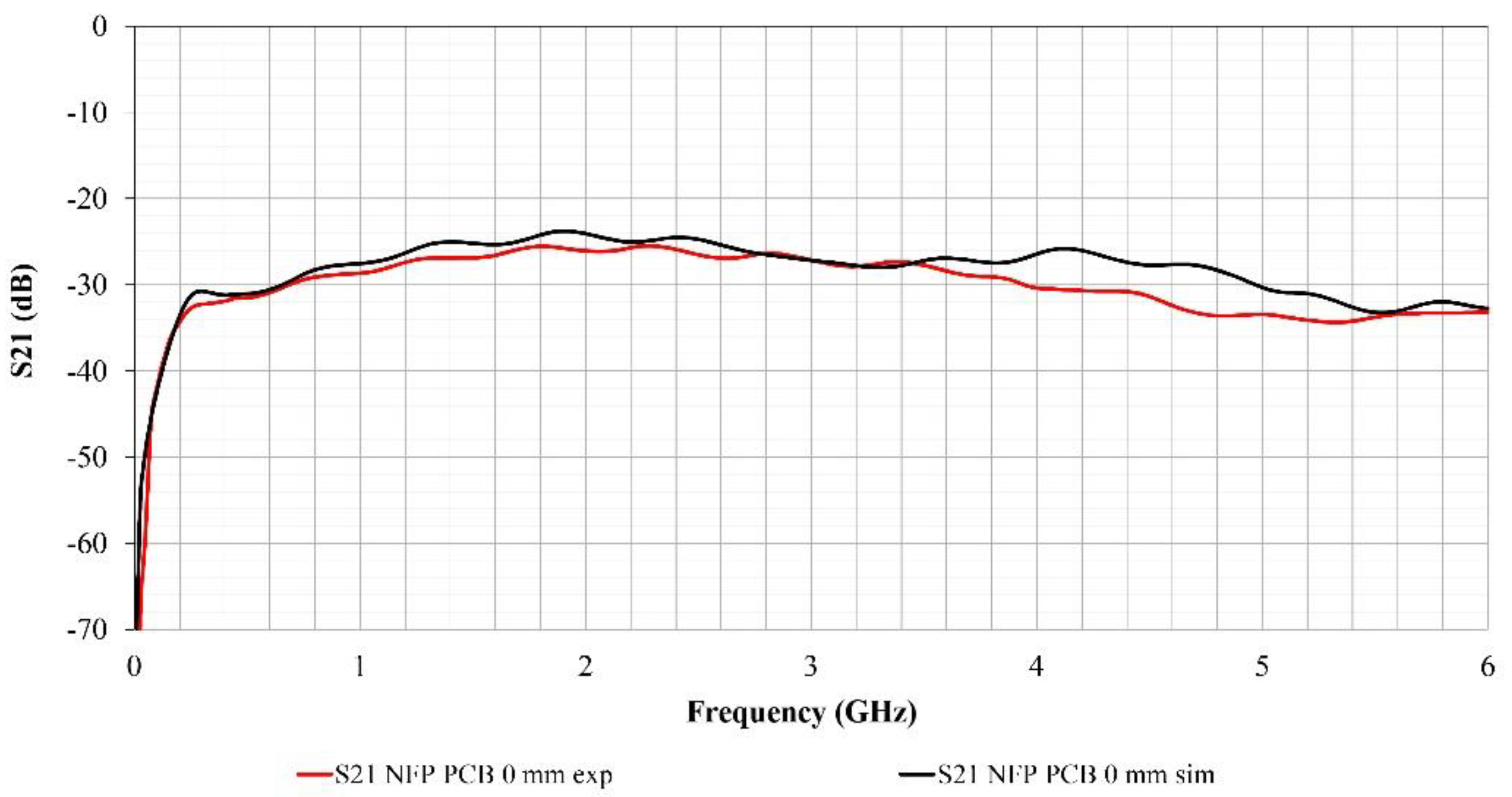
Figure 10 shows measured and simulated S
21 parameter. From
Figure 9, the gain of the NFP-PCB, as well as the bandwidth, is obtained.
Figure 10 shows that the NFP-PCB has almost a flat response from 180 MHz to 6 GHz, with an almost perfect concordance between numerical and experimental S
21 results. There is a small deviation of around 5 dB between 4 and 5 GHz. Moreover, there is a small frequency ripple whose peaks separate in frequency with increasing frequency, possibly due to a small capacitance associated with the assembly that varies little with frequency. It should be noted that the assembly has not been modeled with FEM, neither the VNA nor the surrounding desk. However, these small deviations are not considered critical in the typical NFP-PCB operation. The experimental transmission loss achieves a maximum value of −36.0 dB, whereas the minimum S
21 is −23.6 dB. The numerical results show an average transmission loss of −27.9 dB by considering the flat response bandwidth, whereas the experimental one is −29.7. The obtained results for NFP-PCB are good enough to provide an adequate dynamic range for general measurement equipment intended to RF applications. If a higher gain and higher S
21 would be needed, an external preamplifier module could be introduced between the NFP and the measurement equipment.
Table 3 shows a comparison between the S
21 measurements and FEM numerical results. Both traces show a good agreement since the relative error is lower than 10% in most of the frequency range studied as the relative error shows, having the higher differences in the frequency region from 4.0 GHz up to 5.0 GHz.
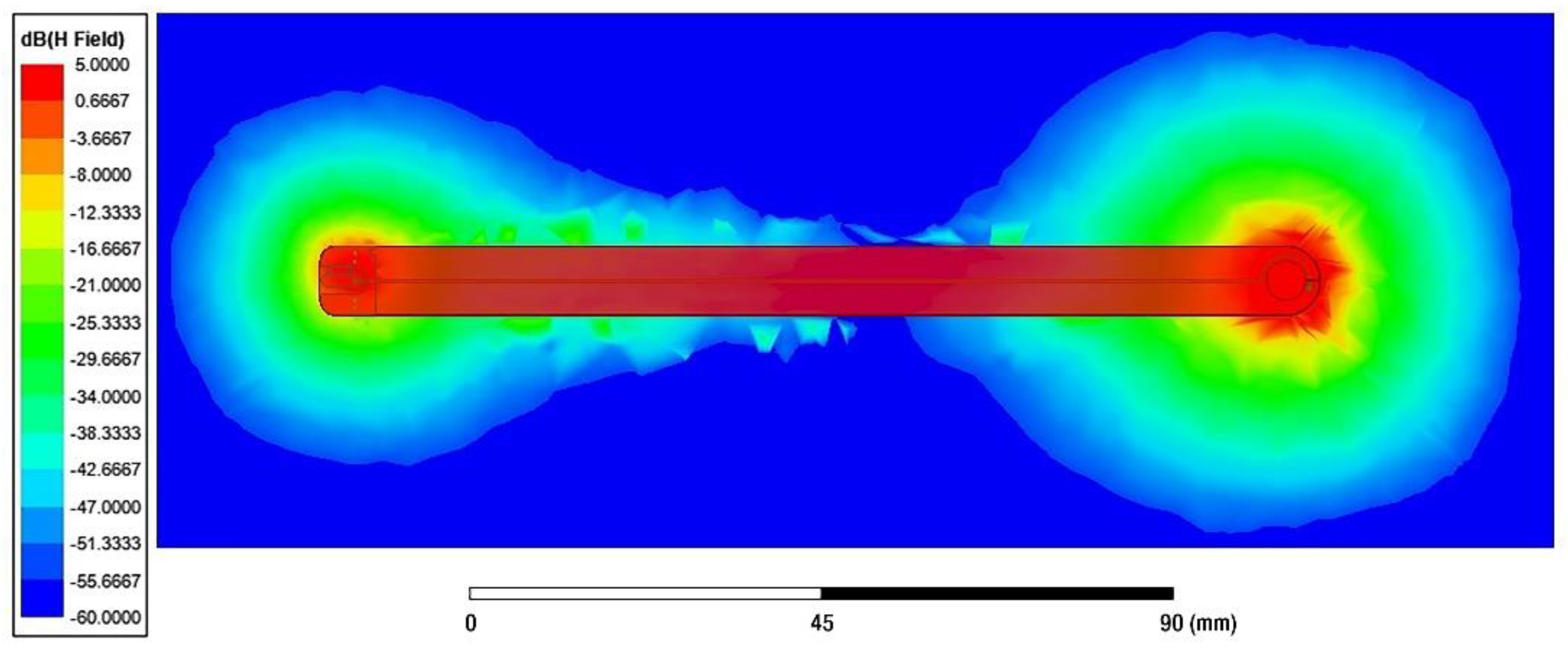
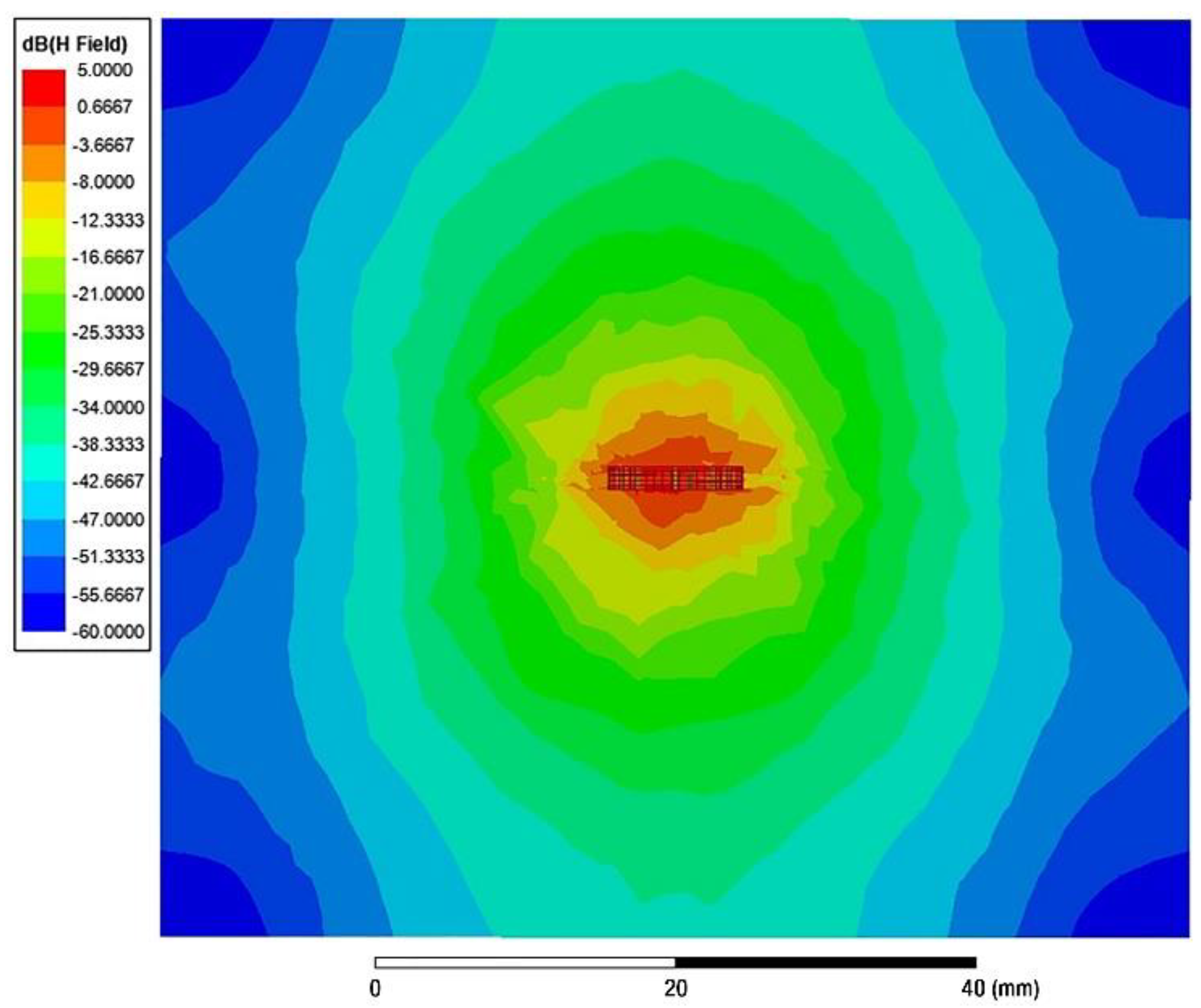
The magnetic field from NFP-PCB is numerically obtained from the FEM simulation,
Figure 11 shows the magnitude of the
H-field (500 MHz) in the x–y plane, the plane that encloses the NFP-PCB substrate.
Figure 12 is the
H-field (500 MHz) in the x–z plane, the plane orthogonal to the NFP-PCB substrate. The
H-field magnitude distribution shows the sensitivity of the probe at different points depending on position, following the reciprocity theorem [
58] the point with highest the radiated
H-field is also the point of highest sensitivity. These are the points near the loop but also the opposite points of the NFP-PCB.
Figure 13 shows the far-field FEM simulation of the NFP-PCB, i.e., the radiation pattern. This approaches closely the radiation pattern of a magnetic dipole, although distorted by the spurious radiation of the feed line. The knowledge of the gain is not relevant for the NFP-PCB operation because it is used in the near field region; however, it is numerically calculated to check the validity of the FEM simulations.
6. NFP-PCB versus Commercial Near-Field Probes
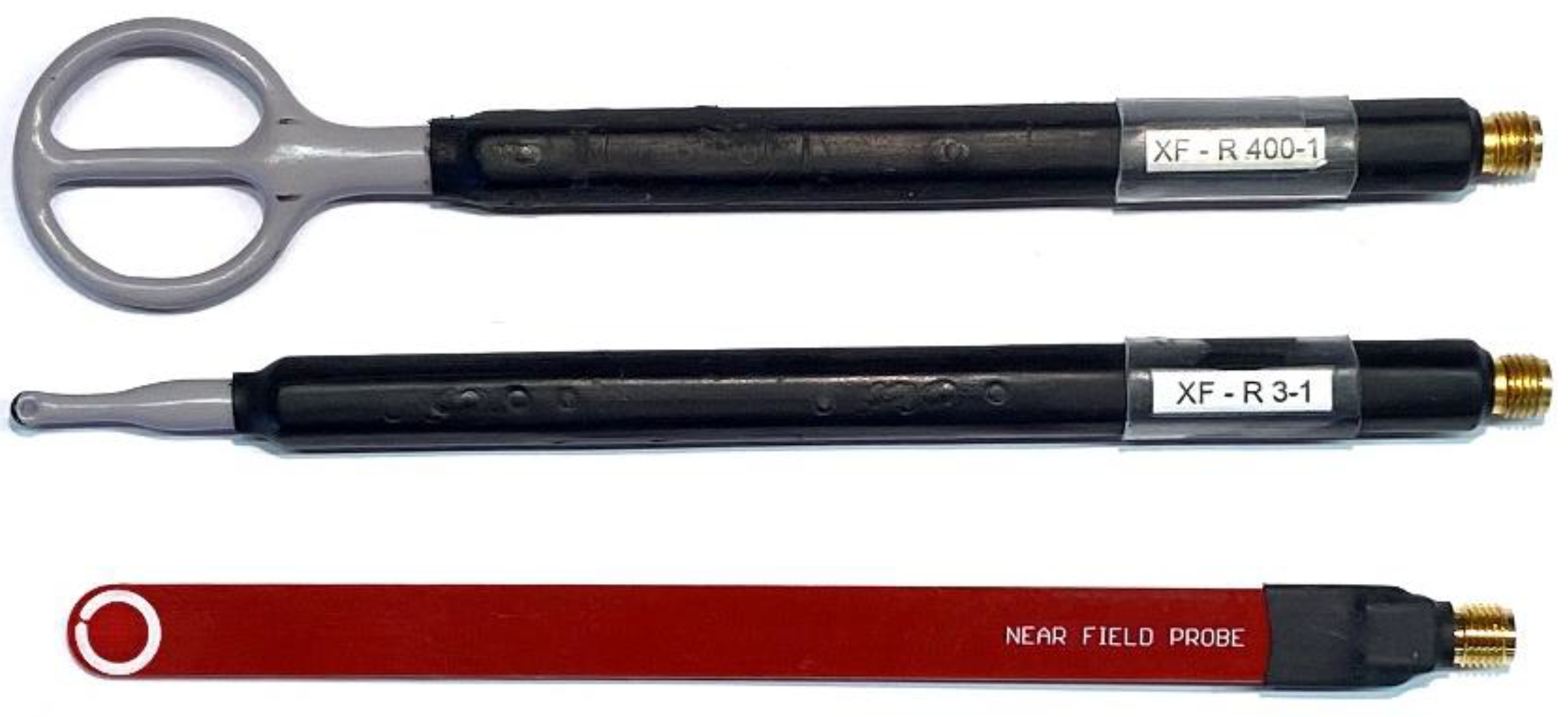
Our measurement setup also allows the measurement of S
21 parameter of other commercial high-quality near-field probes [
45]. These other probes with different loop diameters are also measured in order to compare its performance against our proposed NFP-PCB. Hence, in the following section the S parameters of the designed NFP-PCB are compared with results from XF-R 400-1 NFP which is 25 mm diameter and with XF-R 3-1 NFP which is 3 mm diameter. Due to its large diameter (25 mm) the XF-R 400-1
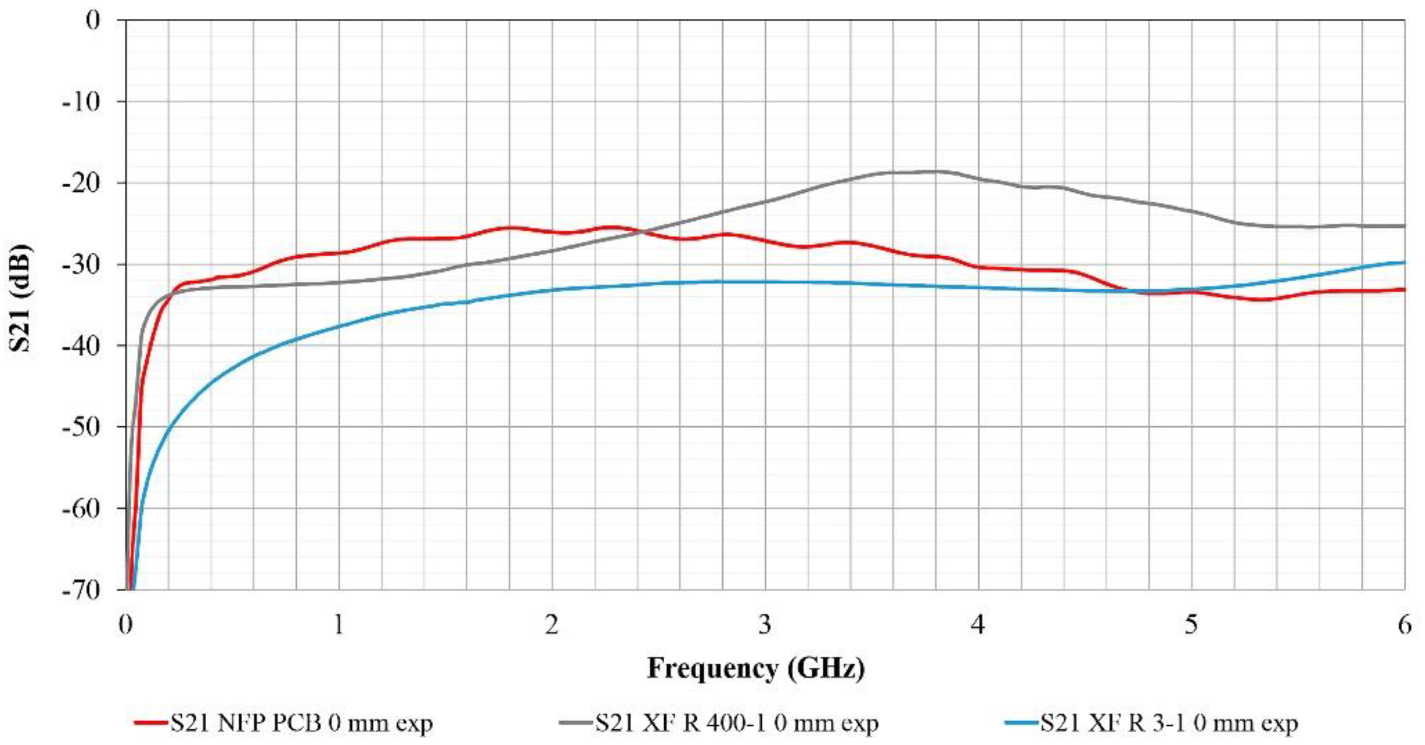
H-field probe is suitable for measurements at distances up to 10 cm around assemblies and devices. The XF-R 3-1 is designed for direct high-resolution measurements of magnetic fields on an assembly, e.g., around the pins and IC cases, conducting paths, decoupling capacitor, and EMC components.
Figure 14 shows a photography of the NFP-PCB and the set of commercial probes selected to carry out the comparison analysis.
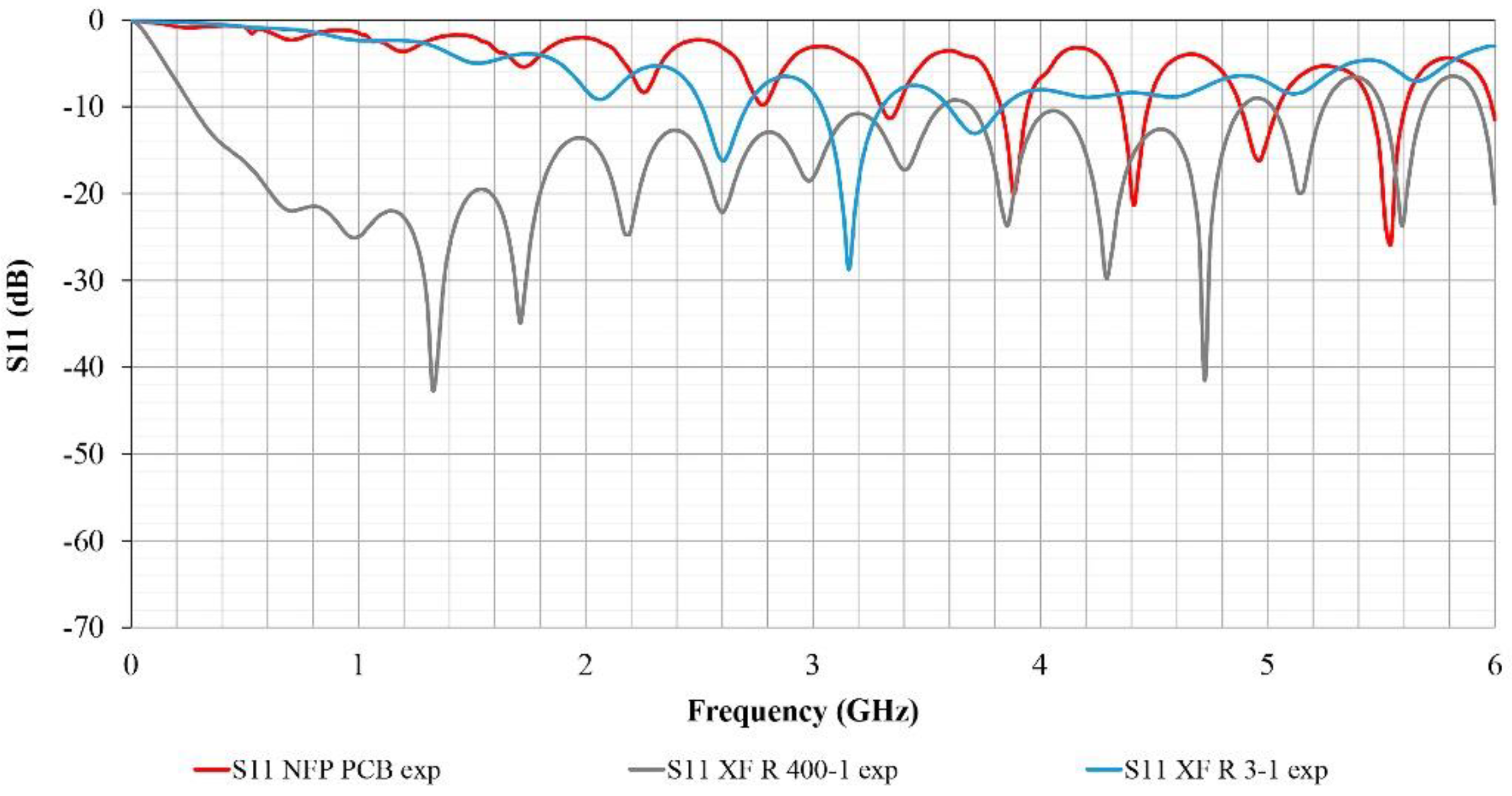
Figure 15 and
Figure 16 show a comparison between the designed NFP-PCB and two commercial probes that are considered as reference values in order to evaluate if the presented probe is suitable for measuring
H-field sources. From the S
11 parameter results, it is possible to observe that the NFP-PCB has a similar response to the commercial probe with lower loop diameter (XF-R 3-1). This is in agreement with the expected results since the other commercial probe (XF-R 400-1) has a diameter loop ten times higher, approximately. The analysis of S
21 parameter shows that the frequency value at which the NFP-PCB starts having a flat response (180 MHz) is significantly similar to the XF-R 400-1 probe. Additionally, both probes have a comparable initial attenuation factor (about −34 dB at 190 MHz). The XF-R 400-1 shows a flat response from 100 MHz to 6 GHz, having an average value of −25.8 dB and reaching a maximum and minimum value of attenuation of −35.5 dB and a −18.6 dB, respectively. As for the XF-R 3-1, its flat response starts at 800 MHz (with an error lower than ±5 dB), and the average value of the flat response is −33.3 dB. This probe provides a minimum value of −39.9 dB and a maximum of −29.8 dB. From this data, it is possible to conclude that the NFP-PCB has a comparable response to both the commercial probes, providing a similar bandwidth and average value than the probe with larger diameter (XF-R 400-1).
7. NFP-PCB as Microwave Antenna
The radiation pattern of build NFP-PCB is measured to compare its performance as non-directive microwave receiver in the measurement of environmental radiation. The NFP-PCB was mounted in the positioner of the anechoic chamber (shown in
Figure 17) and a broadband ridge waveguide antenna was used as probe. The maximum of transmission was measured at 828.5 MHz, which was the frequency used to measure the radiation patterns.
Figure 17 shows the experimental setup to measure the
H-plane radiation pattern.
Figure 18 shows the NFP-PCB radiation patterns, for the horizontal polarized
E-field and vertical polarized
E-field in the
H- and
E-planes. The
E-plane is the plane that contains the loop of the NFP-PCB, and
H-plane is perpendicular to it. The NFP-PCB has two nulls in the
H-plane horizontal polarization 180° between them, as it was expected because it is a loop antenna. However other aspects of a loop antenna are not kept. We measure high levels of vertical polarization in the
E-plane and also nulls in the horizontal polarization
E-plane. This is due to the feed line, and gap, with the multilayer structure of the PCB.
The angular average gain (0−360°) of the NFP-PCB at 828.5 MHz is −4.7 dB with respect the maximum receiving level, with a minimum of −20 dB at one angle, having a standard deviation in 0−360° of 0.6 dB. Thus, the NFP-PCB seems a good antenna to measure environmental microwave levels, combined with a spectrum analyzer.
8. Conclusions
A near field probe NFP-PCB, easy to fabricate is presented. The proposed NFP-PCB was analyzed with FEM numerical simulations and scattering parameters, and near-field spatial distribution was obtained. These parameters are necessary in order to determine its response, bandwidth, and sensitivity. The numerical results obtained with the FEM models were corroborated comparing them to the measurements to verify the design and performance of the NFP-PCB. Therefore, our FEM model reproduces the experimental procedure that is used to evaluate the performance of the NFP-PCB.
The numerical S11 parameter shows a similar response with measurements, but a mismatch between both FEM is noted and measured, caused by a small capacitance that provides a shift in S11 with increasing frequency. In terms of S21, NFP-PCB has almost a flat response from 180 MHz to 6 GHz, with a significant match between numerical and experimental results. The comparison with the high-quality commercial probes shows that the NFP-PCB has a comparable response to both commercial probes. The NFP-PCB has a spatial resolution higher than the XF-R 400-1 (larger loop dimeter) and a lower attenuation ratio than the XF-R 3-1 (lower loop diameter).
Consequently, the performance of the low-cost H-field NFP based on a standard PCB stack-up has been validated since it is shielded against E-fields, showing a significant spatial resolution and sensitivity comparable to high-quality probes studied. Thereby, the proposed NFP-PCB achieves a good cost/accuracy balance, and it could be considered as an interesting debugging tool to carry out pre-compliance measurements.
Finally, the NFP-PCB seems a good far-field receiving antenna for measuring environmental microwave radiation, having a uniform frequency response in the 1–6 GHz band and a non-directive pattern.


 ,
, 


