Article

Adaptive On-Time Control Buck Converter with a Novel Virtual Inductor Current Circuit

1
Department of Electrical Engineering, National Penghu University of Science and Technology, Penghu 880011, Taiwan
2
Department of Electrical Engineering, Chinese Culture University, Taipei 11114, Taiwan
3
Department of Computer Science and Information Engineering, National Taitung University, Taitung 95092, Taiwan
4
Department of Electronic Engineering, National Chin-Yi University of Technology, Taichung 411030, Taiwan
*
Author to whom correspondence should be addressed.
Electronics 2021, 10(17), 2143; https://doi.org/10.3390/electronics10172143
Submission received: 29 July 2021 / Revised: 28 August 2021 / Accepted: 29 August 2021 / Published: 3 September 2021
(This article belongs to the Section Power Electronics)

Abstract

:
This study presents a new virtual inductor current circuit to reduce circuit complexity, which is not necessary to sense inductance current directly. The buck converter was designed to produce an output voltage of 1.0–2.5 V for a 3.0–3.6 V input voltage. The load current range was from 100 mA to 500 mA. It was simulated and verified by SIMPLIS and MathCAD. The simulation results of this buck converter show that the voltage error is within 1%, and the recovery time is smaller than 2 μs for step-up and step-down load transients. Additionally, it achieves less than 26 mV overshoot at full-load step transient response. The circuit topology would be able to fabricate using TSMC 0.35 μm 2P4M CMOS technology. The control mechanism, implementation, and design procedure are presented in this paper.

Graphical Abstract

1. Introduction

Nowadays, the DC–DC buck converter is widely used in mobile phones and other portable electronic devices [1]. In order to improve the competitiveness of products, these portable devices often have more functions, but it also means more power consumption. The power supply of these devices is the battery. Reducing the power consumption of electronic devices can increase the standby time. Therefore, high conversion efficiency and fast response are the key points of power management design [2]. At present, in the power conversion technology, the control mode is roughly divided into voltage mode [3] and current mode [4,5,6,7,8]. As can be seen from Figure 1a, the voltage mode is single-loop control—the voltage loop [3]. In contrast, in Figure 1b, the current mode is dual-loop control—a voltage loop and a current loop. Compared to voltage mode, the current mode has more feedback paths from inductance current; therefore, the current mode has a faster transient response and better voltage regulation than the voltage mode. Therefore, current mode control is widely used in power management IC. With the above two control modes, there are many new control topologies that have been proposed to achieve high speed, low power, high efficiency, and small size. For example, constant on-time (COT) control technology or adaptive on-time (AOT) control technology is used in many converters.
COT control has a feature of high light-load efficiency [9,10,11]. COT control is a variable-frequency control. Under the discontinuous conduction mode (DCM), the switching frequency is naturally lowered, and the efficiency is higher; while the switching frequency increases during the load transient or voltage tracking. The variable switching frequency will affect the overall conversion efficiency due to the switching and conduction losses. The main disadvantage of the COT control scheme is the limitation of the duty cycle. The ON time always follows the preset minimum off time, which depends on the power stage and control logic. This causes the maximum duty cycle to be limited by the ON time during load transient.
Although the variable switching frequency can improve the efficiency in DCM, it will also make the other blocks in the system hard to control the electromagnetic interference (EMI) [12,13,14]. Since the operation principle of the switching power converter is to control the switch on/off, the EMI of the converter is inevitable.
In contrast, in Reference [15], the ON time is designed in inverse/direct proportional to input/output voltage to realize virtually constant-frequency operation, which is known as adaptive on-time (AOT) control. The conventional AOT control scheme is shown in Figure 2. The adaptive on-time control can improve the frequency instability of the COT control. Moreover, there is no subharmonic oscillation issue in AOT current-mode control; therefore, slope compensation is not needed. There are many studies in the literature about the AOT control solutions that have been published [15,16,17,18,19,20,21]. In Reference [17], the on-time AOT control is modulated by the output of the error amplifier rather than fixed voltage. However, the frequency of AOT control is still easily affected by the input voltage and load current changes.
No matter the AOT or COT scheme, as long as it is the current-mode control, the current sensor is usually required [22,23,24,25]. As can be seen from Figure 1b, the Ri represents the current sensor. At present, many current sensors have been proposed [4,12,15,26,27,28,29,30,31,32,33]. Among these current sensors, Hall-effect current sensors are very sensitive to the EMI of the converter [29]. However, the feature of the Hall sensor is to ensure that the power circuit and sensor can be electrically isolated. Aiello et al. [30] use a split-drain MOS transistor (MagFET) to realize an EMI-immune contactless current sensor. The low-cost isolation current sensors based on the giant magnetoresistance effect are proposed in [31,32]. Hall-effect current sensor with EMI immune is proposed in [33].
Typically, contactless current sensors are mainly used for current sensing and measuring in smart grids or in situations where electrical isolation is required [29,30,31,32,33]. Therefore, from the perspective of application and integration, the contactless current sensor solutions may not be suitable for low-power conversion IC.
Studies in the literature [23,24] proposed a sensorless solution, which uses a predictive method to estimate inductor current. The sensing methods proposed in [4,6,15,26,27,28,34] are summarized in what follows.
In Figure 3, the sensing method in [26,34] employed the resistor Rsense in series with the inductor to measure IL by sensing resistive voltage. This sensing technique breaks the origin loop and inserts the sensing component. The disadvantage of this method is that the system power consumption will increase due to the resistor.
Another current-sensing method, shown in Figure 4, is to parallel a set of low-pass filters (i.e., RS, CS) in the inductor L. The disadvantage is that additional components, Rs and Cs, are needed at off-chip [15]. This sensing technique obtains the inductor current information without breaking the origin loop.
In Figure 5, an active current-sensing (ACS) technique was proposed by Chen et al. to sense inductor current [27]. The ACS senses the voltage across the inductor and converts the current information into VSEN. Therefore, the ACS also obtains the inductor current information without breaking the origin loop. Unfortunately, the switching voltage VP, VN will cause the voltage VX to change between 0 and VIN. Due to the large variation of voltage Vx and the off-chip sensing, the sensed VSEN would include some non-ideal effects.
Similarly, Hwang et al. [6] proposed the optimum damping control in Figure 6 to improve the dynamic response. The sensing points are the same [27], and the voltage VX changes between 0 and VIN. Additionally, this sensing technique is a no-break loop method.
Chen et al. [28] proposed an active current-sensing technique for hysteresis-current-controlled (HCC) buck converter, as shown in Figure 7. However, the sample and hold circuits are required in this control scheme, and the ACS will generate sparks, which affect the transient response [4].
This paper presents a novel inductor current sensing circuit. The proposed current sensor obtains the virtual inductor current by switching. The voltage of the proposed sensing point is more stable than the other methods in [4,6,15,26,27,28,34]. Moreover, the circuit is simple and can be integrated into existing control schemes such as AOT and COT. Since the sensor is integrated into the chip, the proposed control scheme provides a more stable control signal with less interference from the off-chip environment.
The paper is organized as follows: Section 2 describes conventional current mode COT/AOT control schemes. Section 3 presents the proposed scheme and implementation. Section 4 introduces the design procedure and modeling analysis with MathCAD. Section 5 shows the SIMPLIS simulation results. Finally, conclusions are given in Section 6.

2. Conventional Control Scheme Descriptions

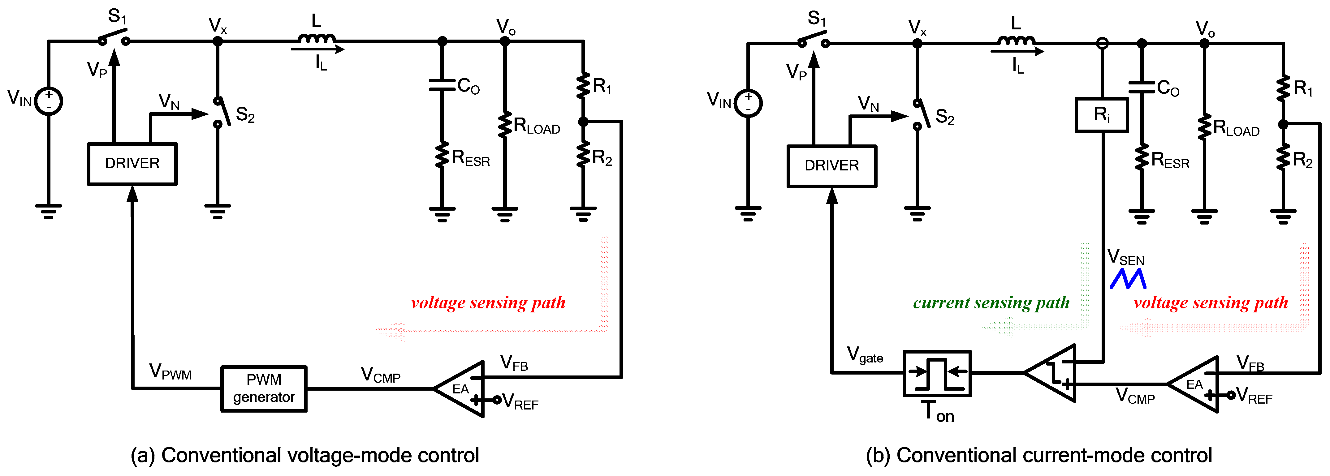
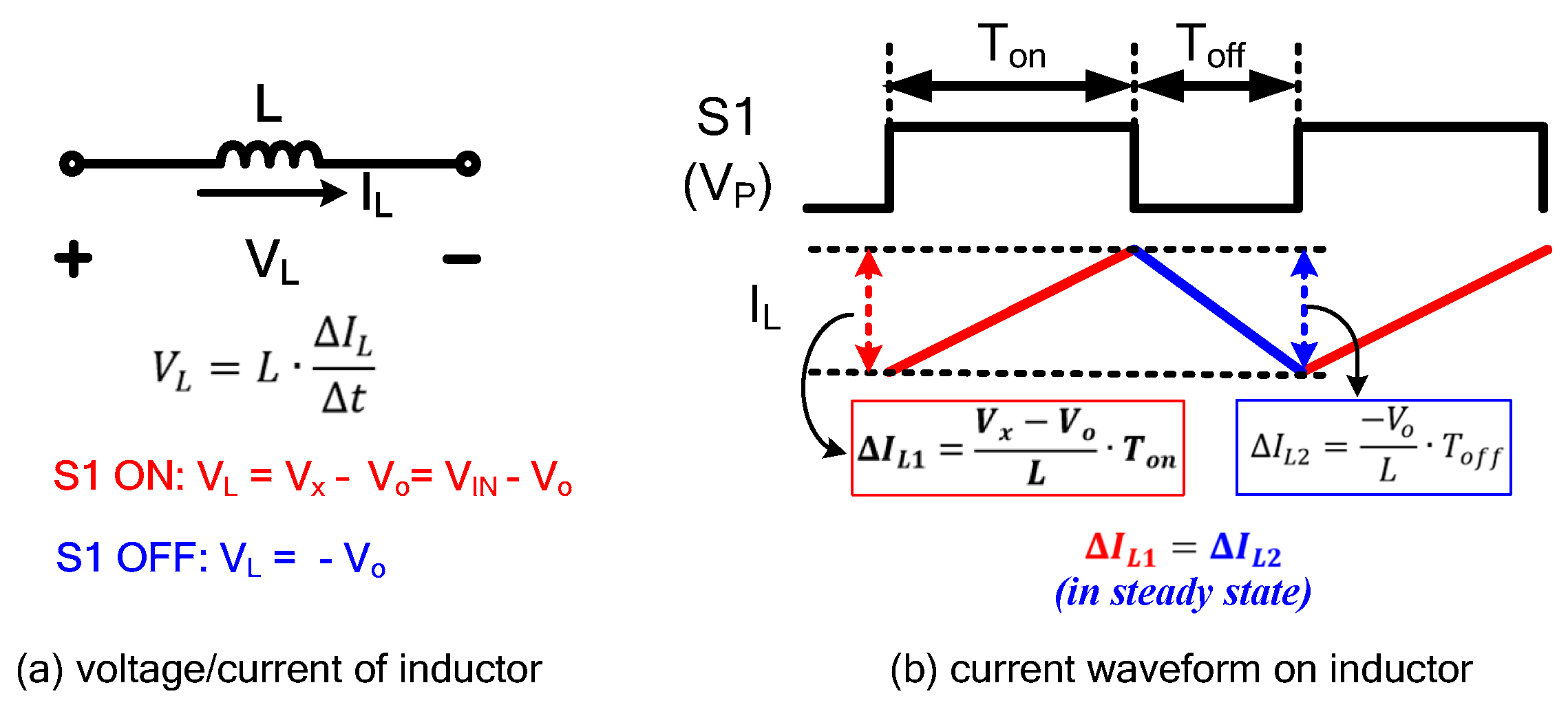
2.1. Current Mode COT (CM-COT) Operating Principle

Figure 1b shows the conventional current mode COT control scheme. The operation of Figure 1b is described as follows: when the triangle wave VSEN is lower the voltage VCMP, the comparator is high. Then, the block, named “Ton” in Figure 1b, produces a constant ON time, which turns on switch S1. The state of switches S1 and S2 are complementary and non-overlapping. This means the control scheme turns on S1 for a fixed ON time and then turns off until the VSEN drops to its limit voltage VCMP, and then turns on S1 again. The block named “EA” means the error amplifier, which includes the trans-conductor and the compensation network. The main purpose of the EA is to regulate Vo and determine OFF time.
In contrast to the pulse width modulation (PWM) control schemes, this control scheme does not need additional slope compensation in the current loop to ensure stability. However, since the switching frequency is allowed to change, the switching control signal looks more jittery in valley current mode control.
Conceptually, in the current control mode, the inductor becomes a controlled current source due to the current loop. Therefore, the whole system becomes a first-order system instead of a second-order system. The phase lag caused by the poles of the power stage is reduced from 180 degrees to 90 degrees. Smaller phase delay makes the compensation of voltage sensing path much easier. The power supply is not so sensitive to variations in capacitance or inductance [35].

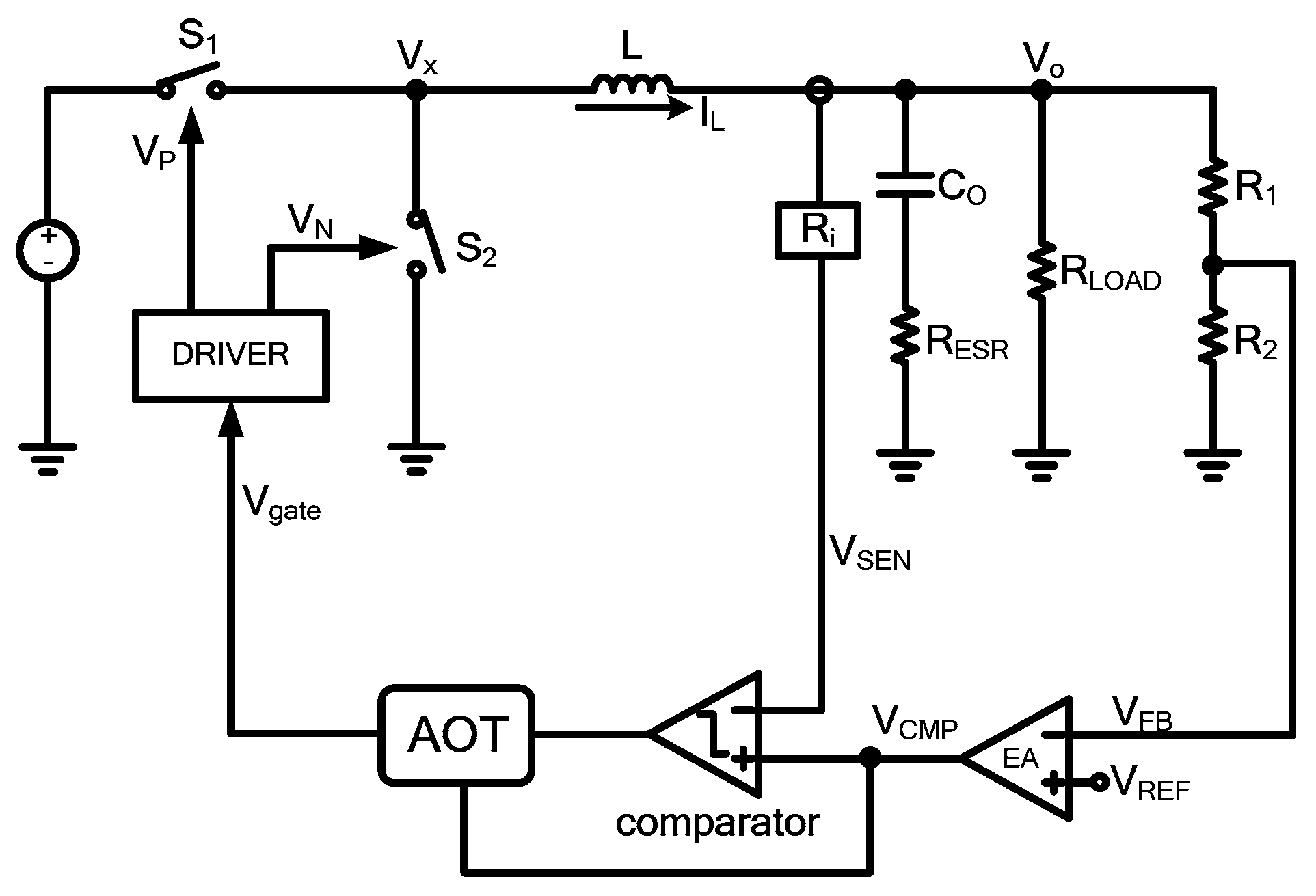
2.2. Current Mode AOT (CM-AOT) Operating Principle

The AOT control scheme in Figure 2 is derived from the COT structure. Therefore, the operation principle of the AOT scheme is roughly the same as the COT scheme. The main difference is that the ON time is controlled by the voltage VCMP, rather than constant.

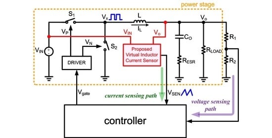
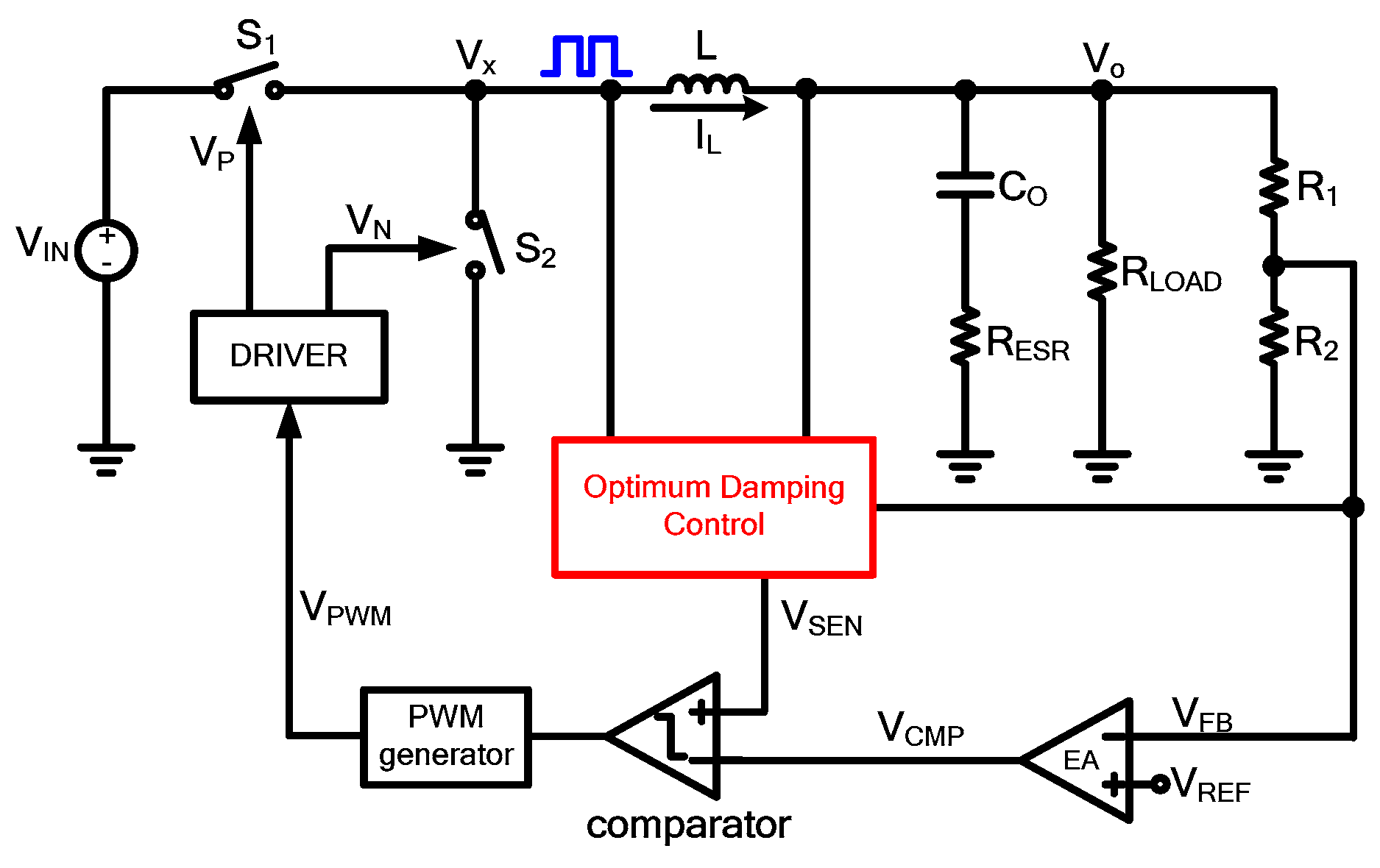
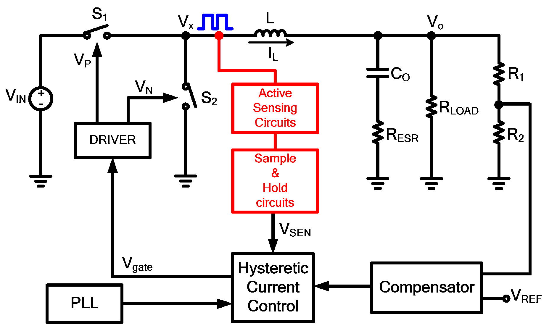
3. Proposed Control Scheme and Implementation

3.1. Operating Principle

Figure 8 shows the proposed control scheme, which is a current mode AOT control. The basic operating principle is the same as the AOT control scheme, described in Section 2.2. Different from [4,6,15,26,27,28], a novel current sensing technique is proposed in this control scheme. In Figure 8, the proposed virtual inductor current (VIC) senses VIN and VO to generate VSEN instead of VX and VO. Since VIN is more stable than VX, the VIC sensing results are expected to be better than [27].

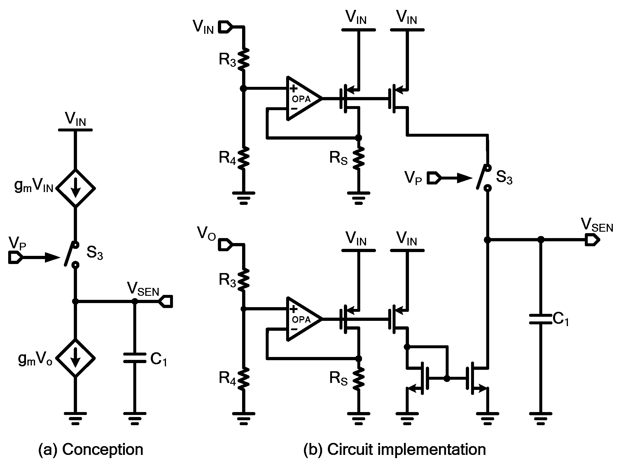
3.2. Proposed Virtual Inductor Current Sensor

The proposed VIC sensor is shown in Figure 9. As is commonly known, the voltage and current on the inductor can be expressed as Equation (1), where L is the inductance, VL and IL are the voltage and current on the inductor, respectively. From Equation (1), the current variation ΔIL will be proportional to VL. Figure 10 illustrates the relation of inductor current and voltage, where S1, Vx, and Vo are shown in Figure 8. Conceptually, IL waveform is similar to current charging/discharging a capacitor. Therefore, as long as Vx, Vo can be included in the charging/discharging current, IL can be converted to VSEN. However, this paper does not sense Vx but senses VIN voltage. Nevertheless, it can also meet the requirements through S3 in Figure 9.
Δ I L = V L L · Δ t
In Figure 9, VIN, VO, VP, VSEN are defined as terminals and represented by I/O pin symbols. In order to clearly present the implementation of the VIC sensor, the VIC sensor is combined into the proposed control scheme and shown in Figure 11.

4. Design Procedure

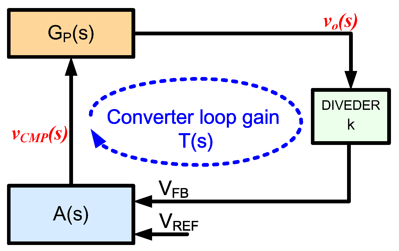
4.1. Buck Converter Modeling

To analyze the stability of the system, we need to obtain the closed-loop transfer function and understand the position of zeros and poles and their influence on the system. The open-loop modeling method for current-mode control is described in [36,37,38]. In fact, it is not easy to develop an accurate small-signal model of current-mode converters. At present, the current-mode converter model proposed by Ridley is the most common small-signal model [39]. In recent years, a more effective and intuitive circuit model for current-mode controls was also proposed by Li et al. [40].
In Figure 12, the modulator Gp(s) consists of the comparator, the inductor, the switches, and the on-time block. In the modeling process, all of them are modeled as a single entity rather than breaking them into parts. By the modeling method described in [39], the transfer function from the signal VCMP to the output signal VO can be presented as Equation (2).
G P ( s ) = v o ( s ) v C M P ( s ) 1 R i · 1 1 + s Q · ω + s 2 ω 2 · R L O A D ( R E S R C o s + 1 ) ( R L O A D + R E S R ) C o s + 1
where R i is the current sensing gain, ω = π T o n   and   Q = 2 π . It is evident from Equation (2) that a double-pole condition may lead to system instability.

4.2. Crossover Frequency fC Determination

Higher bandwidth will have a fast transient response. However, the bandwidth increase will sacrifice the circuit stability, which makes the circuit more susceptible to switching noise. Therefore, how to balance the stability margin and transient response is very important. In fact, due to the current sampling effect, the current-mode control also introduces double poles at ½ fsw [39]. Therefore, for sufficient phase margin, we will often design the crossover frequency at 1/10–1/6 of the switching frequency fsw, as shown in Equation (3).
f c   ( 1 10 ~ 1 6 ) · f S W

4.3. Compensator Design

A(s) is the most critical for loop compensation design, which determines the cross-frequency, DC gain, phase, and gain margin of the voltage loop. To describe the loop gain, Figure 12 is simplified to Figure 13. In Figure 13, the converter loop gain T(s) can be expressed in Equation (4). In this paper, a type II compensation network is used at the output end of the operational amplifier, which is composed of resistance R t , and capacitance C t and C p in parallel. The compensation network combined with an operational amplifier can be expressed as the compensator gain A(s), as shown in Figure 14. The transfer function A(s) is given by Equation (5). In the compensator design procedure, the zero w z is set to cancel the output pole of the peak current-mode buck topology, expressed as Equation (6). The compensation pole w p 2 is set at the lower frequency between the output capacitor ESR zero and 1/2 of the operating frequency. w p 1 is extrapolated to make the feedback system more stable.
T ( s ) = G P ( s ) · A ( s ) · k
A ( s ) = v C M P ( s ) v F B ( s ) = g m · R t h o · ( 1 + s w z ) ( 1 + s w p 1 ) · ( 1 + s w p 2 )
where w z = 1 R t · C t   , w p 1 = 1 R t h o · C t   , w p 2 = 1 R t · C p   .
Set the w z of the compensator to cancel the output pole as follows:
w z = 1 R L O A D · C o u t ,       f z = w z 2 π
Set the w p 2 of the compensator at about 1/2 of the switching frequency, as shown in Equation (7).
w p 2 1 2 · w s = 1 2 · ( 2 π f s w )

4.4. Stability Analysis

Step1: Substitute Table 1 value into Equation (2), then enter the equation into MathCAD and the Bode plot of the G p ( s ) can be drawn in Figure 15, where set Ri = 2, Ton = 0.7 μs. In Figure 15, w p o u t 1 R L O A D · C o   i . e . ,     f p o u t = 4.4   k H z .
Step2: As expressed in Equation (6), set the zero of the compensator f z = f p o u t = 4.4   k H z . From (7), set f p 2 3   M H z . By Equation (5), suppose C t = 200   p F ,   then   R t = 180   k Ω ,     C p = 200   f F can be obtained. The compensator gain is set at 60 dB, which can be adjusted according to the entire loop response. Suppose R t h o = 1   M Ω, then gm = 1 mA/V, and f p 1 800 Hz. Finally, substitute all the above numbers into Equation (5), then enter the equation into MathCAD, and the Bode plot of the compensator is drawn in Figure 16 and Figure 17.
Step3: Enter Equation (4) into MathCAD and substitute k with 0.5. The Bode plot of the loop response T(s) is drawn in Figure 16 and Figure 17. It can be seen that the T(s) phase margin is about 25 degrees, DC gain is about 61 dB, and the crossover frequency fc is about 500 kHz.

5. Simulation Results

5.1. CM-AOT SIMPLIS Schematic Building

In this section, the SIMPLIS tool was used to simulate the proposed CM-AOT scheme. The SIMPLIS schematic is displayed in Figure 18.

5.2. Schematic Stability Analysis

The stability analysis of the proposed scheme was simulated by the SIMPLIS tool, and the results are shown in Figure 19, in which legend label names follow the previous section definition. It can be seen from Figure 19 that the crossover frequency of loop response is about 523 kHz, the phase margin is about 46 degrees, and the DC gain is about 62 dB.
In the previous section, we used MathCAD to draw the Bode plot of the transfer function by numerical approach. However, in this section, we used SIMPLIS to build the circuit architecture and confirm the stability with the Bode plot. In order to find the difference between them, the waveforms in Figure 16, Figure 17, and Figure 19 are redrawn in Figure 20 and Figure 21. From Figure 20 and Figure 21, we found that the results of MathCAD and SIMPLIS have some differences. There are two possible reasons for these differences: 1. Equation (2) has been simplified; 2. the proposed VIC cannot be replaced only by the current gain Ri in Equation (2). Nevertheless, Equation (2) is very close to the real behavior of the system.
From the perspective of stability, A(s) almost determines whether the system is stable or not. As the switching converter contains analog parts and digital parts, the AC stability analysis is not easy. In many cases, non-convergence may occur in AC simulation. To solve the non-convergence issue, the most common method is to run the transient simulation first, then replace the DC point in AC simulation with the DC operation point from transient simulation. At present, many computer-aided design (CAD) software programs, such as LTspice, LTpowerCAD, can help the designers to design the compensator for stability issues. In general, the crossover frequency is higher, and the phase margin is worse. The designer can reduce the loop gain to obtain a good phase margin. However, the loop gain reduction would sacrifice the DC regulation accuracy. The rule of thumb is to recommend the loop gain of 60 dB.
It should be noted that the type selection of compensation network depends on the control mode. In general, the voltage-mode control scheme needs to adopt the type III compensation network, which is fairly complicated. Fortunately, the current-mode control scheme only requires the type II compensation network. Thus, the stability issue would be relieved.

5.3. Transient Performance

Figure 22 shows the load transient waveforms. For the step-up and step-down load current steps between 0.1 A and 0.5 A, the output recovers to within 1% of the expected level 1.8 V in 1.98 μs and 1.6 μs, respectively. In addition, the overshoot and undershoot voltages can also be controlled within 26 mV.
Under 0.5 A load current, the acceptable input range of the proposed converter is 3.0–3.6 V, and the voltage output range is 1.0–2.5 V. The input/output characteristics are shown in Figure 23. Figure 23 shows that the maximum ripple voltage of the converter is 2.5 mV when Vin = 3.6 V and Vo = 2.5 V.
To ensure system reliability, the transient performance of the proposed converter was simulated with the variations of passive/active devices. First, the inductor was simulated with ±5% of variations. The results showed the recovery time would vary from 1.5 μs to 2.0 μs with 4.465 μH to 4.935 μH of the inductance, respectively. Secondly, the recovery time changed from 1.87 μs to 1.3 μs with the gm of the operational amplifier from 0.9 mA/V to 1.1 mA/V, respectively. Thirdly, the time would vary from 1.5 μs to 1.7 μs with −10% to +10% variations of DC gain. These simulation results show that the proposed system is insensitive to the device variations. Therefore, the reliability of the system is expected.

5.4. Load Regulation/Line Regulation

Load regulation is to measure the performance of a power supply. It is the capability to maintain a constant voltage (or current) level on the output despite changes in the load. We expect that a load change causes a small change in output, usually from 3% to 5%. In this paper, under the condition of 1.8 V output voltage with the load current switching from 0.5 A to 0.1 A, the load regulation was calculated by Equation (8). The simulation waveform is shown in Figure 24, and the calculation result is −0.05%.
Load   Regulation   = Δ V o V o @ I L = 0.5 A · 100 %
Line regulation is the ability of a power supply to maintain a constant output voltage despite changes to the input voltage, as shown in Equation (9). The calculation result is close to 0. As this is a system-level simulation, the simulation results of line regulation are meaningless and cannot reflect the real conditions.
Line   Regulation = Δ V o Δ V i n · 100 %

5.5. Performance List

Table 2 presents the performance of the current-mode adaptive on-time control buck converter. The input voltage range is 3.0–3.6 V. When the output voltage is 1.8 V, and the load current steps between 100 mA and 500 mA, the recovery time is smaller than 2 μs. The performance comparisons with reported converters are listed in Table 3.

6. Conclusions

In this study, an adaptive on-time control buck converter with a novel virtual inductor current circuit was proposed. The modeling approach was derived and sketched by MathCAD and SIMPLIS. This paper describes the design parameters and design procedure in detail. Moreover, a system-level circuit topology was build and verified by SIMPLIS. This study proposed the implementation of the VIC circuit that is compatible with the existing AOT architecture. The sensing point of VIC is more stable than that of ACS in [27]. Hence, the overall performance would be better than [27]. The proposed buck converter can be implemented with TSMC 0.35 μm 2P4M CMOS processes further.

Author Contributions

H.-H.C., conceptualized and designed the prototype, simulated the whole system, wrote original draft preparation; H.-L.C. performed the verification and revised the paper; Y.-H.F. analyzed the data; S.-F.W. wrote the paper. All authors have read and agreed to the published version of the manuscript.

Funding

This research was funded by Ministry of Science and Technology, Taiwan, under Grants MOST 110-2222-E-346-001.

Conflicts of Interest

The authors declare no conflict of interest.

References

  1. Chen, J.J.; Yang, F.C.; Chen, C.C. A new monolithic fast-response buck converter using spike-reduction current-sensing circuits. IEEE Trans. Ind. Electron. 2008, 55, 1101–1111. [Google Scholar] [CrossRef]
  2. Chen, J.J.; Hwang, Y.S.; Hwang, B.H.; Jhang, Y.C.; Ku, Y.T. A dual-mode fast-transient average-current-mode buck converter without slope-compensation. In Proceedings of the 2018 7th International Symposium on Next Generation Electronics(ISNE) Conference, Taipei, Taiwan, 7–9 May 2018. [Google Scholar]
  3. Huang, Q.; Zhan, C.; Burm, J. A 30-MHz Voltage-Mode Buck Converter Using Delay-Line-Based PWM Control. IEEE Trans. Circuits Syst. II 2018, 65, 1659–1663. [Google Scholar] [CrossRef]
  4. Chen, J.J.; Hwang, Y.S.; Chen, J.H.; Ku, Y.T.; Yu, C.C. A New Fast-Response Current-Mode Buck Converter with Improved I2-Controlled Techniques. IEEE Trans. Very Large Scale Integr. (VLSI) Syst. 2018, 26, 903–911. [Google Scholar] [CrossRef]
  5. Chen, J.J.; Hwang, Y.S.; Lin, J.Y.; Ku, Y.T. A Dead-Beat-Controlled Fast-Transient-Response Buck Converter with Active Pseudo-Current-Sensing Techniques. IEEE Trans. Very Large Scale Integr. (VLSI) Syst. 2019, 27, 1751–1759. [Google Scholar] [CrossRef]
  6. Hwang, Y.S.; Chen, J.J.; Ku, Y.T.; Yang, J.Y. An Improved Optimum-Damping Current-Mode Buck Converter with Fast-Transient Response and Small-Transient Voltage Using New Current Sensing Circuits. IEEE Trans. Ind. Electron. 2021, 68, 9505–9514. [Google Scholar] [CrossRef]
  7. Chen, W.W.; Chen, J.F.; Liang, T.J.; Wei, L.C.; Ting, Y.W. Designing a Dynamic Ramp with an Invariant Inductor in Current-Mode Control for an On-Chip Buck Converter. IEEE Trans. Power Electron. 2014, 29, 750–758. [Google Scholar] [CrossRef]
  8. Saini, D.K.; Reatti, A.; Kazimierczuk, M.K. Average Current-Mode Control of Buck DC-DC Converter with Reduced Control Voltage Ripple. In Proceedings of the IECON 2016 42nd Annual Conference of the IEEE Industrial Electronics Society, Florence, Italy, 23–26 October 2016. [Google Scholar]
  9. Zhong, S.; Shen, Z. A Hybrid Constant On-Time Mode for Buck Circuits. Electronics 2021, 10, 930. [Google Scholar] [CrossRef]
  10. Lin, Y.-C.; Chen, C.-J.; Chen, D.; Wang, B. A Ripple- Based Constant On-Time Control with Virtual Inductor Current and Offset Cancellation for DC Power Converters. IEEE Trans. Power Electron. 2012, 27, 4301–4310. [Google Scholar] [CrossRef]
  11. Nien, C.-F.; Chen, D.; Hsiao, S.-F. A Novel Adaptive Quasi-Constant On-Time Current-Mode Buck Converter. IEEE Trans. Power Electron. 2017, 32, 8124–8133. [Google Scholar] [CrossRef]
  12. Nguyen, V.H.; Huynh, H.A.; Kim, S.Y.; Song, H. Active EMI Reduction Using Chaotic Modulation in a Buck Converter with Relaxed Output LC Filter. Electronics 2018, 7, 254. [Google Scholar] [CrossRef] [Green Version]
  13. Chen, W.C.; Chen, H.C.; Chien, M.W.; Chou, Y.W.; Chen, K.H.; Lin, Y.H.; Lee, C.C. Pseudo-constant switching frequency in on-time controlled buck converter with predicting correction techniques. IEEE Trans. Power Electron. 2016, 31, 3650–3662. [Google Scholar] [CrossRef]
  14. Chen, W.C.; Lin, K.L.; Chen, K.H.; Lin, Y.H.; Tsai, T.Y.; Huang, C.C.; Yang, C.C. A pseudo fixed switching frequency 2 kHz/A in optimum on-time control buck converter with predicting correction technique for EMI solution. In Proceedings of the 2014 IEEE International Symposium on Circuits and Systems (ISCAS), Melbourne, Australia, 1–5 June 2014; pp. 946–949. [Google Scholar]
  15. Zhen, S.; Zeng, P.; Chen, J.; Zhou, W.; Wang, J.; Luo, P.; Zhang, B. Transient Response Improvement of DC-DC Converter by Current Mode Variable on Time Control. In Proceedings of the 2018 IEEE 61st International Midwest Symposium on Circuits and Systems (MWSCAS), Windsor, ON, Canada, 5–8 August 2018. [Google Scholar]
  16. Lin, H.-C.; Fung, B.-C.; Chang, T.-Y. A current mode adaptive on-time control scheme for fast transient DC-DC converters. In Proceedings of the 2008 IEEE International Symposium on Circuits and Systems, Seattle, WA, USA, 18–21 May 2008. [Google Scholar]
  17. Zhen, S.; Zhou, S.; Zeng, L.; Yang, M.; Ming, X.; Luo, P.; Zhang, B. Variable on time controlled buck converter for DVS applications. In Proceedings of the IECON 2017-43rd Annual Conference of the IEEE Industrial Electronics Society, Beijing, China, 29 October–1 November 2017. [Google Scholar]
  18. Bari, S.; Li, Q.; Lee, F.C. Fast Adaptive On Time Control for Transient Performance Improvement. In Proceedings of the IEEE Applied Power Electronics Conference and Exposition (APEC), Charlotte, NC, USA, 15–19 March 2015. [Google Scholar]
  19. Liu, P.-J.; Kuo, M.-H. Adaptive On-Time Buck Converter with Wave Tracking Reference Control for Output Regulation Accuracy. Energies 2021, 14, 3809. [Google Scholar] [CrossRef]
  20. Tsai, C.H.; Chen, B.M.; Li, H.L. Switching Frequency Stabilization Techniques for Adaptive On-Time Controlled Buck Converter with Adaptive Voltage Positioning Mechanism. IEEE Trans. Power Electron. 2016, 31, 443–451. [Google Scholar] [CrossRef]
  21. Bari, S.; Li, Q.; Lee, F.C. A New Fast Adaptive On-Time Control for Transient Response Improvement in Constant On-Time Control. IEEE Trans. Power Electron. 2018, 33, 2680–2689. [Google Scholar] [CrossRef]
  22. Aiello, O.; Fiori, F. A new mirroring circuit for power MOS current sensing highly immune to EMI. Sensor 2013, 13, 1856–1871. [Google Scholar] [CrossRef] [PubMed] [Green Version]
  23. Min, R.; Chen, C.; Zhang, X.; Zou, X.; Tong, Q.; Zhang, Q. An Optimal Current Observer for Predictive Current Controlled Buck DC-DC Converters. Sensors 2014, 14, 8851–8868. [Google Scholar] [CrossRef] [Green Version]
  24. Tong, Q.; Chen, C.; Zhang, Q.; Zou, X. A Sensorless Predictive Current Controlled Boost Converter by Using an EKF with Load Variation Effect Elimination Function. Sensors 2015, 15, 9986–10003. [Google Scholar] [CrossRef] [Green Version]
  25. Aiello, O.; Fiori, F. Current sensing circuit for DC-DC converters based on the miller effect. In Proceedings of the 2013 International Conference on Applied Electronics (AE), Pilsen, Czech Republic, 10–11 September 2013; pp. 1–4. [Google Scholar]
  26. Sheehan, R. Understanding and Applying Current-Mode Control Theory. Texas Instruments Technical Document Application Reports. Literature Number: SNVA555. 2007. Available online: https://www.ti.com/lit/pdf/snva555 (accessed on 31 August 2021).
  27. Chen, J.J.; Hwang, Y.S.; Ku, Y.T.; Li, Y.H.; Chen, J.A. A Current-Mode-Hysteretic Buck Converter with Constant-Frequency-Controlled and New Active-Current-Sensing Techniques. IEEE Trans. Power Electron. 2021, 36, 3126–3134. [Google Scholar] [CrossRef]
  28. Chen, J.-J. An Active Current-Sensing Constant-Frequency HCC Buck Converter using Phase-Frequency-Locked Techniques. IEEE Trans. Ultrason. Ferroelectr. Freq. Control 2008, 55, 761–769. [Google Scholar] [CrossRef]
  29. Aiello, O. Hall-Effect Current Sensors Susceptibility to EMI: Experimental Study. Electronics 2019, 8, 1310. [Google Scholar] [CrossRef] [Green Version]
  30. Aiello, O.; Fiori, F. A New MagFET-Based Integrated Current Sensor Highly Immune to EMI. Elsevier Microelectron. Reliab. 2013, 53, 573–581. [Google Scholar] [CrossRef]
  31. Ouyang, Y.; He, J.; Hu, J.; Wang, S.X. A current sensor based on the giant magnetoresistance effect: Design and potential smart grid applications. Sensors 2012, 12, 15520–15541. [Google Scholar] [CrossRef]
  32. Jantaratana, P.; Sirisathitkul, C. Low-cost sensors based on the GMI effect in recycled transformer cores. Sensors 2008, 8, 1575–1584. [Google Scholar] [CrossRef] [PubMed] [Green Version]
  33. Dalessandro, L.; Karrer, N.; Kolar, J.W. High-Performance Planar Isolated Current Sensor for Power Electronics Applications. IEEE Trans. Power Electron. 2007, 22, 1682–1692. [Google Scholar] [CrossRef]
  34. Song, C. Accuracy Analysis of Constant-On Current-Mode DC-DC Converters for Powering Microprocessors. In Proceedings of the 2009 Twenty-Fourth Annual IEEE Applied Power Electronics Conference and Exposition, Washington, DC, USA, 21 March 2009. [Google Scholar]
  35. Zhang, H.J. Modeling and Loop Compensation Design of Switching Mode Power Supplies. LINEAR Technology Application Note 149, January 2015. Available online: https://www.analog.com/media/en/technical-documentation/application-notes/an149fa.pdf (accessed on 31 August 2021).
  36. Li, J.; Lee, F.C. New modeling approach and equivalent circuit representation for current-mode control. IEEE Trans Power Electron. 2010, 25, 1218–1230. [Google Scholar]
  37. Enrique, J.-M.; Barragán, A.-J.; Durán, E.; Andújar, J.-M. Theoretical Assessment of DC/DC Power Converters’ Basic Topologies. A Common Static Model. Appl. Sci. 2018, 8, 19. [Google Scholar] [CrossRef] [Green Version]
  38. Suntio, T. Dynamic Modeling and Analysis of PCM-Controlled DCM-Operating Buck Converters—A Reexamination. Energies 2018, 11, 1267. [Google Scholar] [CrossRef] [Green Version]
  39. Ridley, R.B. An Accurate and Practical Small-Signal Model for Current-Mode Control. Available online: www.ridleyengineering.com (accessed on 1 September 2021).
  40. Li, J. Current-Mode Control: Modeling and Its Digital Application. Ph.D. Dissertation, Virginia Polytechnic Institute and State University, Blacksburg, VA, USA, 2009. [Google Scholar]
  41. Jiang, C.R.; Chai, C.C.; Han, C.X.; Yang, Y.T. A high performance adaptive on-time controlled valley-current-mode DCDC buck converter. J. Semicond. 2020, 41, 062406. [Google Scholar] [CrossRef]
Figure 1. Voltage-/current-mode control schemes.
Electronics 10 02143 g001
Figure 2. Conventional AOT control scheme.
Electronics 10 02143 g002
Figure 3. AOT scheme with the inductor current-sensing resistor.
Electronics 10 02143 g003
Figure 4. AOT scheme with the Rs, Cs sensing components.
Electronics 10 02143 g004
Figure 5. Hysteretic scheme with active current-sensing technique.
Electronics 10 02143 g005
Figure 6. PWM control scheme with rail-to-rail current-sensing technique.
Electronics 10 02143 g006
Figure 7. Active current-sensing constant-frequency HCC buck converter.
Electronics 10 02143 g007
Figure 8. Proposed control scheme.
Electronics 10 02143 g008
Figure 9. Proposed virtual inductor current sensor.
Electronics 10 02143 g009
Figure 10. Voltage current relationship of inductor.
Electronics 10 02143 g010
Figure 11. Proposed VIC sensor in control scheme.
Electronics 10 02143 g011
Figure 12. CM-AOT modeling.
Electronics 10 02143 g012
Figure 13. Block diagram for feedback loop.
Electronics 10 02143 g013
Figure 14. Compensator gain.
Electronics 10 02143 g014
Figure 15. Bode plot of Gp(s) for buck converter.
Electronics 10 02143 g015
Figure 16. Gain response of Gp(s), A(s), and T(s).
Electronics 10 02143 g016
Figure 17. Phase response of Gp(s), A(s), and T(s).
Electronics 10 02143 g017
Figure 18. The SIMPLIS simulation schematic.
Electronics 10 02143 g018
Figure 19. Bode plot results with SIMPLIS.
Electronics 10 02143 g019
Figure 20. Gain comparison between MathCAD and SIMPLIS.
Electronics 10 02143 g020
Figure 21. Phase comparison between MathCAD and SIMPLIS.
Electronics 10 02143 g021
Figure 22. (a) Load current step-up behavior; (b) Load current step-down behavior.
Electronics 10 02143 g022aElectronics 10 02143 g022b
Figure 23. Input/output characteristics.
Electronics 10 02143 g023
Figure 24. Waveform of load regulation.
Electronics 10 02143 g024
Table 1. Simulation condition.
ComponentValueUnit
RLOAD3.6Ω
Co10μF
L4.7μH
RESR5
Table 2. Performance summary.
Input voltage3.0–3.6 V
Output voltage1.0–2.5 V
Max. output ripple
(@Vin = 3.6 V, Vo = 2.5 V)
2.51 mV
Max. load current0.5 A
Inductor/DCR *4.7 μH/30 mΩ
Output capacitor/ESR10 μF/5 mΩ
Transient response
@ Vo = 1.8 V
100 mA to 500 mA1.98 μs
500 mA to 100 mA1.6 μs
Transient voltage
@ Vo = 1.8 V
Overshoot23 mV
Undershoot26 mV
* DCR: the DC resistance of inductor.
Table 3. Performance comparisons with reported converters.
References2018 [15]2020 [41]2021 [27]This work
Resultssimulationsimulationmeasurementsimulation
Control schemeAOTAOTHysteretic PLLAOT
Process (μm)0.350.180.350.35 **
Input voltage (V)123.3–5.03.3–3.63.0–3.6
Output voltage (V)1.21.80.9–2.51.0–2.5
Inductor (μH)11.54.74.7
Output capacitor (μF)47201010
Max. load current (mA)50002000600500
Load current step (mA)4000800400400
Undershoot/overshoot (mV)20/2613/1430/6023/26
Recovery time (μs) (rise/fall)<36/22.6/2.21.98/1.6
** This work is a system-level simulation with SIMPLIS.
Publisher’s Note: MDPI stays neutral with regard to jurisdictional claims in published maps and institutional affiliations.

