
LogicSNN: A Unified Spiking Neural Networks Logical Operation Paradigm


Abstract
:1. Introduction
2. Related Work
3. Methods
3.1. Definition and Encoding Method of Logical Operation
3.2. Spike Neuron Model and Network Structure
3.2.1. Spike Neuron Model
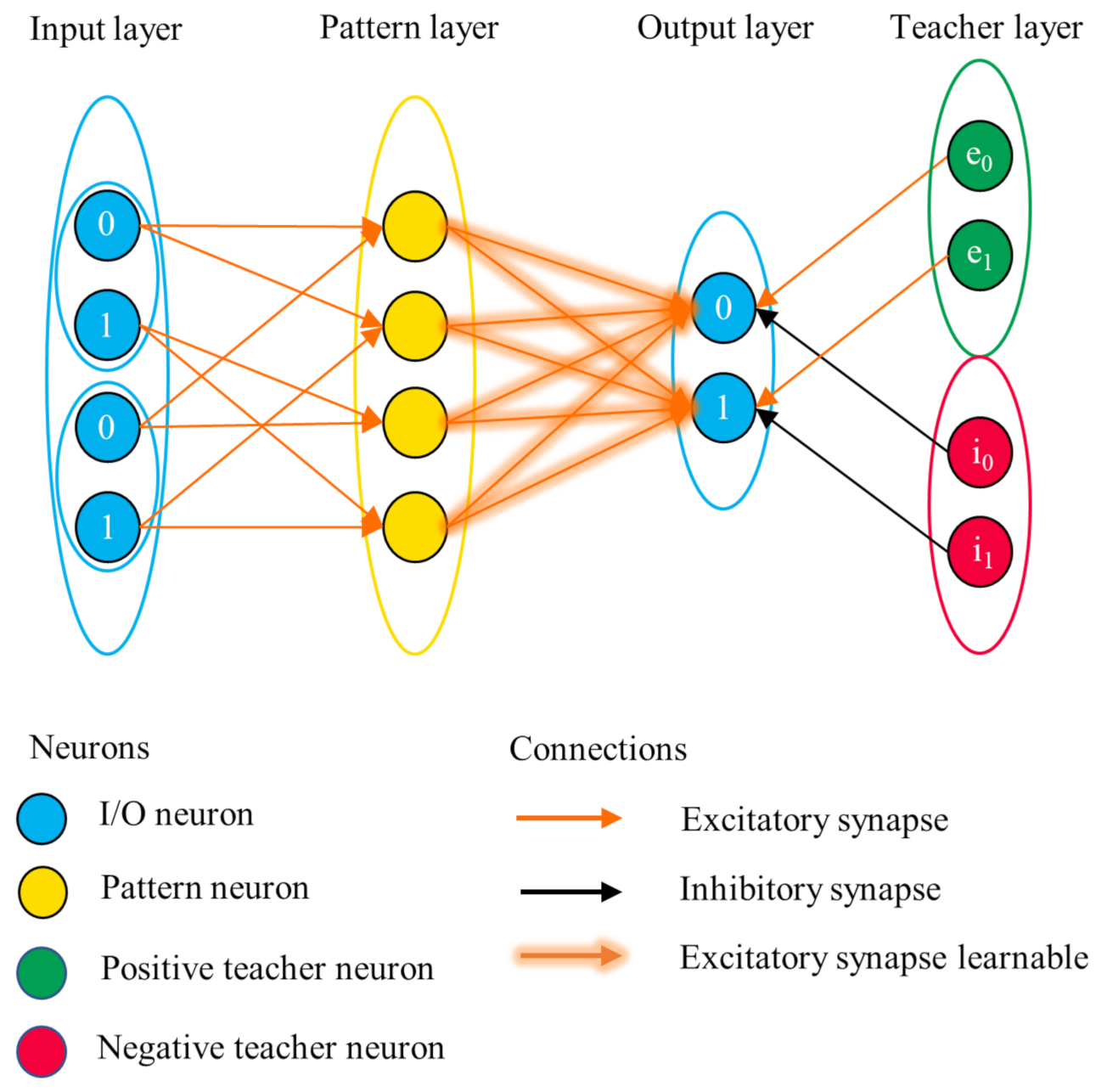
3.2.2. Network Structure
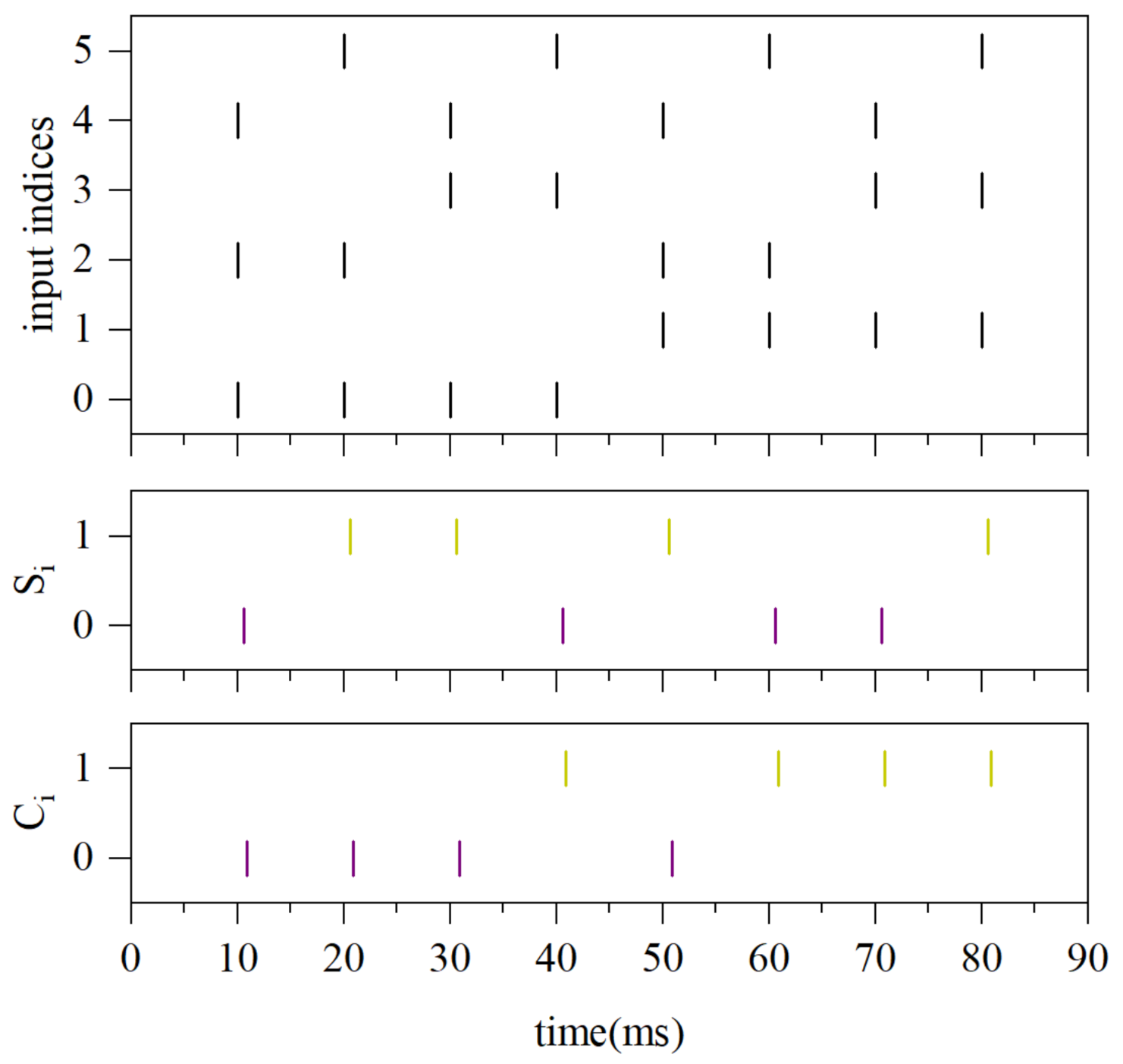
3.3. Training Method
4. Experiments and Results
- (1)
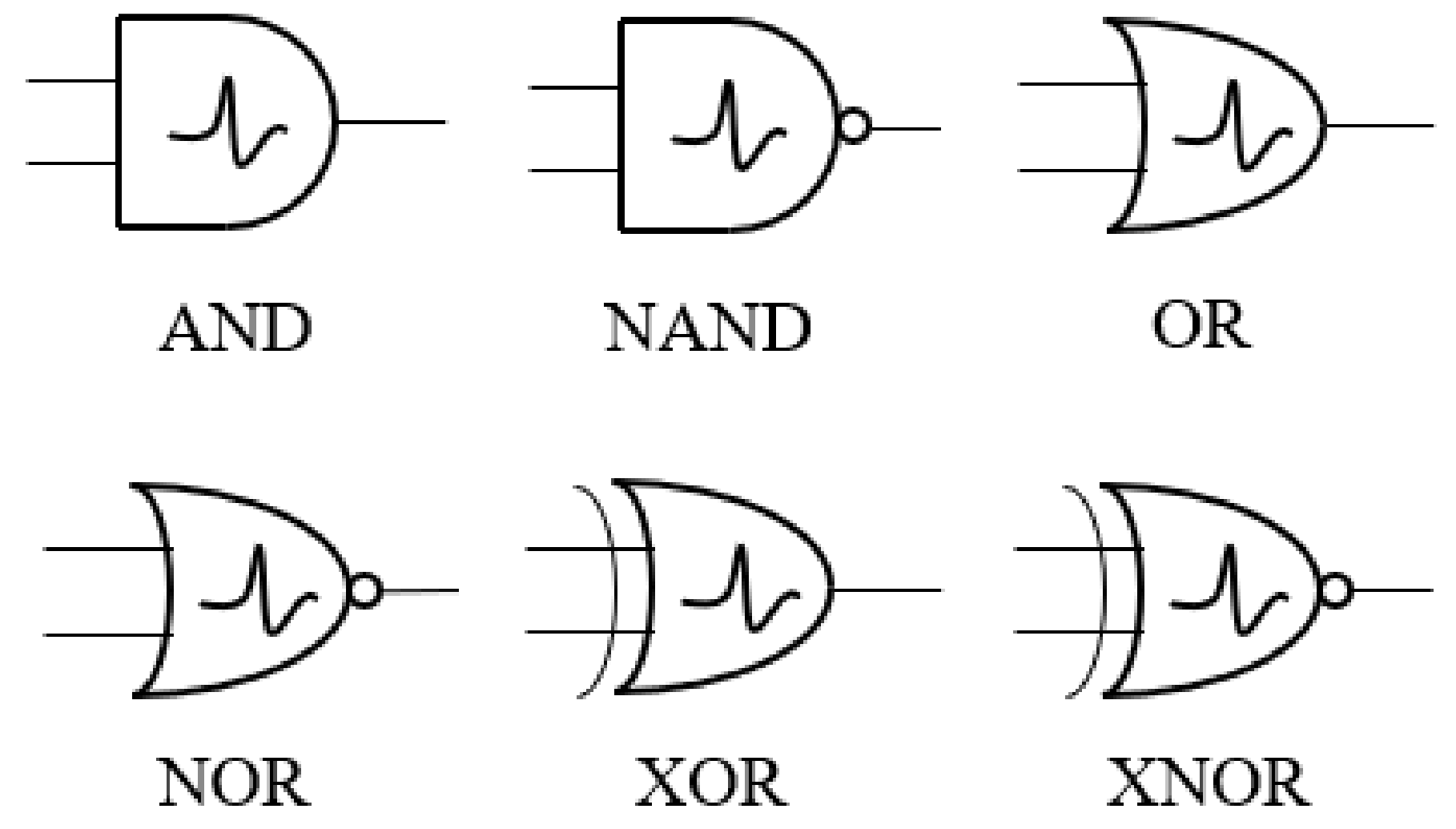
- The construction, learning and testing of six kinds of basic SNN binary logical operation modules: AND, OR, NAND, NOR, XOR, XNOR, in Section 4.1.
- (2)
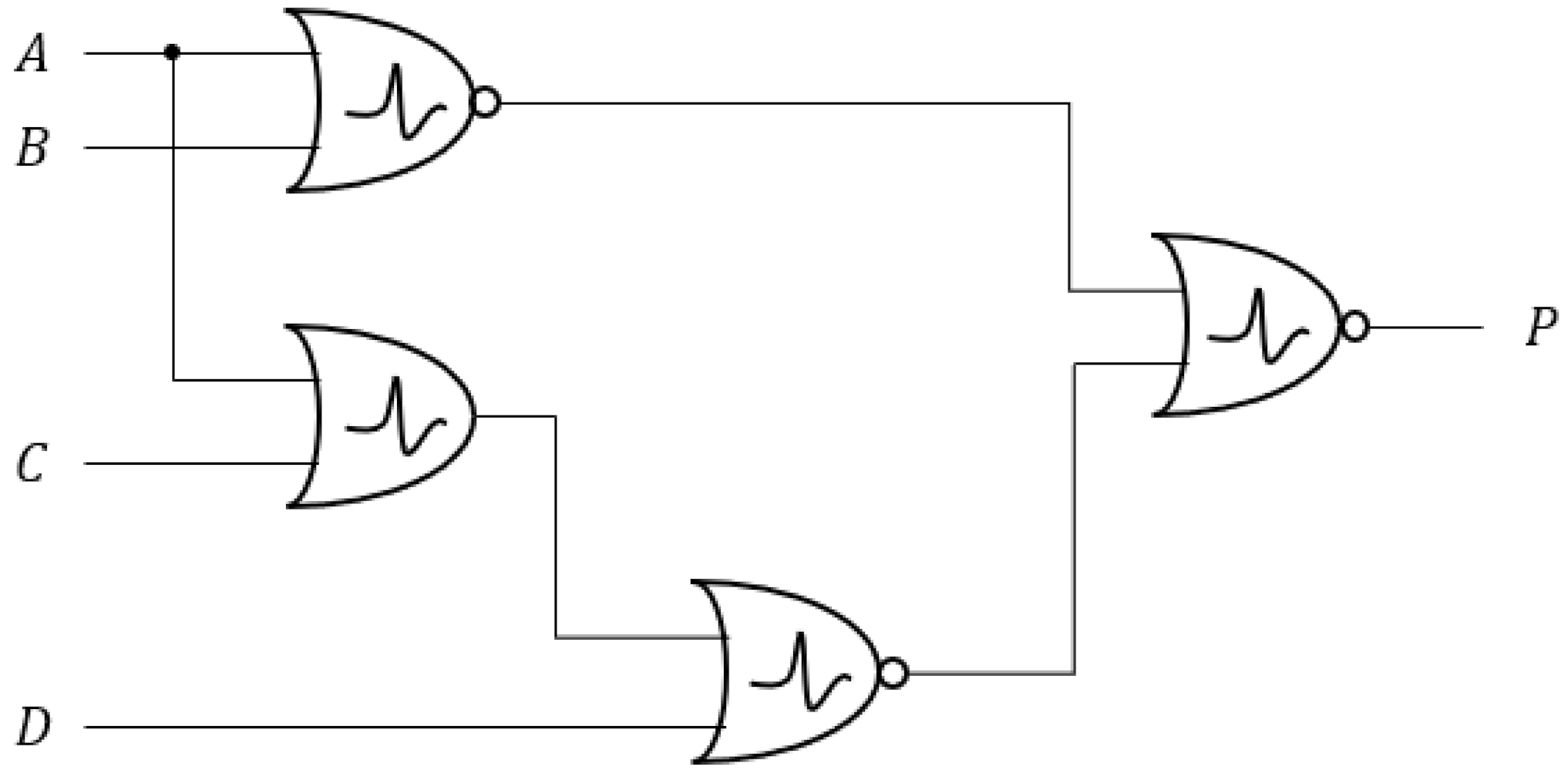
- The building and testing of simple combinational logic networks in Section 4.2: the rounding logic network of 8421-binary-coded decimal (BCD) code, half adder, full adder, which takes the basic SNN binary logical operation modules in (1) as the basic components.
4.1. Basic SNN Binary Logical Operation Modules
4.2. Combinational Logic Networks
4.2.1. Rounding Logic Network of 8421-BCD Code
4.2.2. Half Adder and Full Adder
5. Discussion
6. Conclusions
Author Contributions
Funding
Acknowledgments
Conflicts of Interest
References
- Cook, S.J.; Jarrell, T.A.; Brittin, C.A.; Wang, Y.; Bloniarz, A.E.; Yakovlev, M.A.; Nguyen, K.C.; Tang, L.T.H.; Bayer, E.A.; Duerr, J.S.; et al. Whole-animal connectomes of both Caenorhabditis elegans sexes. Nature 2019, 571, 63–71. [Google Scholar] [CrossRef] [PubMed]
- Brittin, C.A.; Cook, S.J.; Hall, D.H.; Emmons, S.W.; Cohen, N. A multi-scale brain map derived from whole-brain volumetric reconstructions. Nature 2021, 591, 105–110. [Google Scholar] [CrossRef] [PubMed]
- Maass, W. Networks of spiking neurons: The third generation of neural network models. Neural Netw. 1997, 10, 1659–1671. [Google Scholar] [CrossRef]
- McCulloch, W.S.; Pitts, W. A logical calculus of the ideas immanent in nervous activity. Bull. Math. Biophys. 1943, 5, 115–133. [Google Scholar] [CrossRef]
- Goldental, A.; Guberman, S.; Vardi, R.; Kanter, I. A computational paradigm for dynamic logic-gates in neuronal activity. Front. Comput. Neurosci. 2014, 8, 52. [Google Scholar] [CrossRef] [PubMed] [Green Version]
- Vogels, T.P.; Abbott, L.F. Signal propagation and logic gating in networks of integrate-and-fire neurons. J. Neurosci. 2005, 25, 10786–10795. [Google Scholar] [CrossRef] [PubMed]
- Adonias, G.L.; Yastrebova, A.; Barros, M.T.; Balasubramaniam, S.; Koucheryavy, Y. A logic gate model based on neuronal molecular communication engineering. In Proceedings of the 4th Workshop on Molecular Communications, Linz, Austria, 16–18 April 2019. [Google Scholar]
- Adonias, G.L.; Yastrebova, A.; Barros, M.T.; Koucheryavy, Y.; Cleary, F.; Balasubramaniam, S. Utilizing neurons for digital logic circuits: A molecular communications analysis. IEEE Trans. Nanobiosci. 2020, 19, 224–236. [Google Scholar] [CrossRef] [PubMed]
- Adonias, G.L.; Siljak, H.; Barros, M.T.; Marchetti, N.; White, M.; Balasubramaniam, S. Reconfigurable Filtering of Neuro-Spike Communications Using Synthetically Engineered Logic Circuits. Front. Comput. Neurosci. 2020, 14, 91. [Google Scholar] [CrossRef] [PubMed]
- Wang, Z.; Gao, S.; Wang, J.; Yang, H.; Todo, Y. A dendritic neuron model with adaptive synapses trained by differential evolution algorithm. Comput. Intell. Neurosci. 2020, 2020, 2710561. [Google Scholar] [CrossRef] [PubMed] [Green Version]
- Boole, G. An Investigation of the Laws of thought, on Which Are Founded the Mathematical Theories of Logic and Probabilities; Walton and Maberly; Dublin University Press: London, UK, 1854. [Google Scholar]
- Peizhi, L. Digital Circuit and Logic Design; Beijing University of Posts and Telecommunications Press: Beijing, China, 2009. [Google Scholar]
- Gerstner, W.; Kistler, W.M.; Naud, R.; Paninski, L. Neuronal Dynamics: From Single Neurons to Networks and Models of Cognition; Cambridge University Press: Cambridge, UK, 2014. [Google Scholar]
- Su, J.; Vargas, D.V.; Sakurai, K. One Pixel Attack for Fooling Deep Neural Networks. IEEE Trans. Evol. Comput. 2019, 23, 828–841. [Google Scholar] [CrossRef] [Green Version]
- Wade, J.; McDaid, L.; Santos, J.; Sayers, H. SWAT: A Spiking Neural Network Training Algorithm for Classification Problems. IEEE Trans. Neural Netw. 2010, 21, 1817–1830. [Google Scholar] [CrossRef] [PubMed] [Green Version]
- Hebb, D.O. The Organisation of Behaviour: A Neuropsychological Theory; Science Editions: New York, NY, USA, 1949. [Google Scholar]
- Caporale, N.; Dan, Y. Spike Timing—Dependent Plasticity: A Hebbian Learning Rule. Annu. Rev. Neurosci. 2008, 31, 25–46. [Google Scholar] [CrossRef] [PubMed] [Green Version]
- Song, S.; Miller, K.D.; Abbott, L.F. Competitive Hebbian learning through spike-timing-dependent synaptic plasticity. Nat. Neurosci. 2000, 3, 919–926. [Google Scholar] [CrossRef] [PubMed]
- Stimberg, M.; Brette, R.; Goodman, D.F. Brian 2, an intuitive and efficient neural simulator. Elife 2019, 8, e47314. [Google Scholar] [CrossRef] [PubMed]
- Goodman, D.; Brette, R. The Brian simulator. Front. Neurosci. 2009, 3, 26. [Google Scholar] [CrossRef] [PubMed] [Green Version]


| A | B | ||||||
|---|---|---|---|---|---|---|---|
| 0 | 0 | 0 | 0 | 1 | 1 | 0 | 1 |
| 0 | 1 | 0 | 1 | 1 | 0 | 1 | 0 |
| 1 | 0 | 0 | 1 | 1 | 0 | 1 | 0 |
| 1 | 1 | 1 | 1 | 0 | 0 | 0 | 1 |
| −50 mV | −80 mV | 5 ms | 1 | 0.005 | * = 0.005 |
| ∗ 1.05 = 0.00525 | 20 ms | 20 ms | 4 | 1400, 2000 | 5 ms |
| 8421-BCD | Decimal Number | 8421-BCD | Decimal Number |
|---|---|---|---|
| 0000 | 0 | 0101 | 5 |
| 0001 | 1 | 0110 | 6 |
| 0010 | 2 | 0111 | 7 |
| 0011 | 3 | 1000 | 8 |
| 0100 | 4 | 1001 | 9 |
| A | B | C | D | P | A | B | C | D | P |
|---|---|---|---|---|---|---|---|---|---|
| 0 | 0 | 0 | 0 | 0 | 0 | 1 | 0 | 1 | 1 |
| 0 | 0 | 0 | 1 | 0 | 0 | 1 | 1 | 0 | 1 |
| 0 | 0 | 1 | 0 | 0 | 0 | 1 | 1 | 1 | 1 |
| 0 | 0 | 1 | 1 | 0 | 1 | 0 | 0 | 0 | 1 |
| 0 | 1 | 0 | 0 | 0 | 1 | 0 | 0 | 1 | 1 |
| A | B | S | C |
|---|---|---|---|
| 0 | 0 | 0 | 0 |
| 0 | 1 | 1 | 0 |
| 1 | 0 | 1 | 0 |
| 1 | 1 | 0 | 1 |
| 0 | 0 | 0 | 0 | 0 |
| 0 | 0 | 1 | 1 | 0 |
| 0 | 1 | 0 | 1 | 0 |
| 0 | 1 | 1 | 0 | 1 |
| 1 | 0 | 0 | 1 | 0 |
| 1 | 0 | 1 | 0 | 1 |
| 1 | 1 | 0 | 0 | 1 |
| 1 | 1 | 1 | 1 | 1 |
Publisher’s Note: MDPI stays neutral with regard to jurisdictional claims in published maps and institutional affiliations. |
© 2021 by the authors. Licensee MDPI, Basel, Switzerland. This article is an open access article distributed under the terms and conditions of the Creative Commons Attribution (CC BY) license (https://creativecommons.org/licenses/by/4.0/).
Share and Cite
Mo, L.; Wang, M. LogicSNN: A Unified Spiking Neural Networks Logical Operation Paradigm. Electronics 2021, 10, 2123. https://doi.org/10.3390/electronics10172123
Mo L, Wang M. LogicSNN: A Unified Spiking Neural Networks Logical Operation Paradigm. Electronics. 2021; 10(17):2123. https://doi.org/10.3390/electronics10172123
Chicago/Turabian StyleMo, Lingfei, and Minghao Wang. 2021. "LogicSNN: A Unified Spiking Neural Networks Logical Operation Paradigm" Electronics 10, no. 17: 2123. https://doi.org/10.3390/electronics10172123
APA StyleMo, L., & Wang, M. (2021). LogicSNN: A Unified Spiking Neural Networks Logical Operation Paradigm. Electronics, 10(17), 2123. https://doi.org/10.3390/electronics10172123