Article

Digital Suppression of EMI-Induced Errors in a Baseband Acquisition Front-End including Off-the-Shelf, EMI-Sensitive Operational Amplifiers

Department of Electronics and Telecommunications (DET), Politecnico di Torino, 10129 Torino, Italy
*
Author to whom correspondence should be addressed.
Electronics 2021, 10(17), 2096; https://doi.org/10.3390/electronics10172096
Submission received: 6 August 2021 / Revised: 23 August 2021 / Accepted: 24 August 2021 / Published: 29 August 2021
(This article belongs to the Special Issue Electromagnetic Interference and Compatibility, Volume II)

Abstract

:
In this paper, the susceptibility to Electromagnetic Interference (EMI) of an analog signal acquisition front-end (AFE) due to EMI distortion in opamp-based pre-conditioning amplifiers is addressed. More specifically, the possibility to correct EMI-induced errors in the digital domain by post-processing the acquired digital waveforms is discussed and experimentally demonstrated for the first time with reference to an AFE based on EMI-sensitive, off-the-shelf operational amplifiers mounted on a specific EMI test PCB. Extensive experimental characterization in the presence of continuous wave and amplitude modulated EMI reveals the superior immunity to EMI of the proposed AFE and the robustness of the approach.

1. Introduction

The susceptibility to Electromagnetic Interference (EMI) of analog integrated circuits (ICs) [1,2,3] is a major threat to the reliability and to the security of analog signal acquisition front-ends (AFEs) [4,5] in traditional applications such as automotive [6,7,8], biomedical [9] and power electronics [10], as well as in emerging wearables [11], smart grid [12] and Internet of Things (IoT) sensor nodes [13], which are operating in a more and more over-crowded electromagnetic environment [14,15,16,17,18].
Among the most detrimental effects of EMI, the rectification of radio frequency (RF) disturbances superimposed onto the input voltages of integrated operational amplifiers (opamps), has been extensively investigated in the literature over the last two decades [19,20,21,22,23,24,25,26], and several countermeasures have been proposed.
In most EMI-robust opamp circuits proposed so far in the literature [26,27,28,29,30,31,32,33,34,35,36,37,38,39,40,41,42,43,44], a reduced susceptibility to EMI is achieved at integrated circuit level either by filtering or by filtered replica stages [29,30,35,36,37,40,41,43], or by ad-hoc input differential stages, in which the EMI-induced offset voltage and the low-frequency demodulated components resulting from RF rectification are mitigated by active device degeneration [28,39], or ideally cancelled by compensating asymmetries in EMI propagation [30,31,32,38] or, finally, by the compensation of different nonlinear mechanisms [21,30,33,34,37,41,42].
In spite of many significant improvements observed in the last years [26,27,28,29,30,31,32,33,34,35,36,37,38,39,40,41,42,43] the EMI-robust opamp circuits presented to date still suffer of several limitations. First, EMI immunity invariably requires non-conventional topologies and careful ad hoc analog design; second, it can be easily impaired by process variations and device mismatch; third, it is often traded off with baseband performance and/or with chip area and power. Last but not least, the solutions proposed so far are not easily portable across technology nodes and are unsuitable to integration in emerging nanoscale technologies and/or in ultra-low voltage (ULV), ultra-low power (ULP) systems.
In this scenario, considering that many challenges and limitations of analog circuits have been recently addressed by digital-based or digitally assisted solutions [17,45,46], rather than by analog design, the possibility to tackle the adverse effects of EMI in opamp-based sensor readouts in the digital domain, regardless of the intrinsic susceptibility to EMI of the analog circuits topologies, would be highly desirable. Under this perspective, a digital-based approach aimed to address the susceptibility to EMI of opamp-based acquisition front-ends (AFEs) at system-level has already been proposed in [47] and demonstrated by circuit simulations.
In this paper, more theoretical insight into the EMI effect compensation approach originally proposed in [47] and on its calibration is provided. Moreover, the design and the implementation of the proposed technique on an AFE based on commercial off-the-shelf EMI-sensitive opamps is discussed and the effectiveness of the approach in retrieving the nominal information content from EMI-corrupted signals is demonstrated for the first time by extensive experimental characterization under continuous wave (CW) and amplitude-modulated (AM) EMI excitation.
The rest of the paper has the following structure: in Section 2, the cancellation of EMI-induced errors by digital post-processing is discussed from a theoretical point of view, and the solution proposed in [47] is revised. In Section 3, the implementation of the proposed solution in an AFE based on off-the-shelf components mounted on a printed circuit board (PCB) is discussed and in Section 4, the effectiveness of the solution is then experimentally verified under standard direct power injection (DPI) test conditions [48]. Some concluding remarks are finally drawn in Section 5.

2. Acquisition Front-End Immunity by Digital Post-Processing

In this paper, the susceptibility to EMI of a generic baseband AFE for sensor readout including an anti-aliasing filter, an opamp-based conditioning amplifier, a sample-and-hold (S/H) circuit and an analog-to-digital converter (ADC), as depicted in Figure 1, is considered. For the sake of simplicity, and without loss of generality, the conditioning amplifier is assumed to be connected in the voltage follower configuration, which has been found to be particularly susceptible to EMI compared to other opamp-based circuits [19,21].
With reference to the AFE in Figure 1, RF interference above tens of MHz is not properly suppressed by the anti aliasing filter due parasitics, and out-of-band disturbances leak to the input of the opamp-based conditioning amplifier [4]. Due to the nonlinear characteristics of the opamp input stage [21], such disturbances are rectified, giving rise to a low frequency spurious component Δ v EMI which corrupts the nominal opamp output voltage and hence the ADC digital output stream.
While the opamp susceptibility is normally addressed either by on-chip filtering or by ad hoc opamp circuits [26,27,28,29,30,31,32,33,34,35,36,38,39,40,41,42], the reconstruction of the original information from the sensor by post-processing the corrupted digital output stream from the ADC will be addressed in this paper.
As far as legitimate sensor signals and demodulated EMI components are added together in the ADC output and have similar spectral characteristics, they cannot be discriminated unless further information on the nominal signal and on the EMI-induced errors is available. In this paper, such additional information is gained by simultaneous acquisitions of the same sensor by two independent channels of the AFE, as illustrated in Figure 2, where the conditioning amplifiers used in each channel are both susceptible to EMI, but in a different way, as better explained in what follows. Indeed, this approach is similar to sensor fusion [49], in which the same input quantity is measured by different sensors, differently affected by non-idealities, whose outputs are digitally processed to get an estimate of the input which is much more accurate than the individual sensor outputs.

2.1. Proposed Sensor Readout

To implement the concept outlined above, the sensor readout architecture in Figure 2 is exploited. Here, the same analog signal v x ( t ) is pre-conditioned by two amplifiers with identical baseband characteristics and a different behavior in the presence of EMI. In practice, this can be easily obtained in CMOS (BJT) technology using one conditioning amplifier based on an nMOS-input (npn-input) opamp, which is characterized by a positive EMI-induced offset, and one conditioning amplifier based on a pMOS-input (pnp-input) opamp, which shows a negative EMI-induced offset under the same EMI excitation. The outputs v 1 ( t ) and v 2 ( t ) of the two opamps are then simultaneously sampled and acquired by the same ADC. An estimate of the samples of the legitimate input signal is finally obtained from the corrupted samples acquired by the ADC as explained in what follows.

2.2. EMI Distortion in the Conditioning Amplifiers

When the AFE in Figure 2 operates in an EMI-free environment, both the conditioning amplifiers provide substantially the same correct output signal v 1 ( t ) = v 2 ( t ) = v x ( t ) , being v x ( t ) the signal from the sensor. By contrast, in the presence of EMI, the outputs v 1 ( t ) and v 2 ( t ) of the two amplifiers in Figure 2 are corrupted by different EMI-dependent error terms Δ v EMI , 1 ( t ) and Δ v EMI , 2 ( t ) so that:
v 1 ( t ) = v x ( t ) + Δ v EMI , 1 ( t )
v 2 ( t ) = v x ( t ) + Δ v EMI , 2 ( t ) .
Under the hypothesis of narrowband EMI (this hypothesis is met in most practical cases, and in particular for wireless communication signals interfering with a baseband sensor readout, which is the most common interference scenario.) around frequency f 0 B 1 , B 2 , where B 1 and B 2 are the gain-bandwidth products of the opamps, the EMI waveform v EMI ( t ) can described in terms of its complex envelope (Hilbert transform) v ˜ EMI ( t ) as:
v EMI ( t ) = v ˜ EMI ( t ) e j 2 π f 0 t = v EMI , c ( t ) cos ( 2 π f 0 t ) v EMI , s ( t ) sin ( 2 π f 0 t )
where
v EMI , c ( t ) = v ˜ EMI ( t ) v EMI , s ( t ) = v ˜ EMI ( t ) .
Moreover, for practical EMI excitations v EMI ( t ) with a root-mean-square (r.m.s.) value up to several hundreds of millivolts, EMI demodulation in conditioning amplifiers can be conveniently described by second-order nonlinear circuit analysis, as detailed in [4], and EMI-induced error terms can be consequently expressed as:
Δ v EMI , 1 ( t ) = K 1 | v ˜ EMI ( t ) | 2 Δ v EMI , 2 ( t ) = K 2 | v ˜ EMI ( t ) | 2
in which the constant factors K i ( i = 1 , 2 ) depend on the topology and on the design parameters of the opamp input stages and on the negative feedback configuration. In particular, it has been observed [21] that K i is positive (negative) in opamps based on an nMOS (pMOS) input differential pair.

2.3. EMI Compensation by Digital Post-Processing

In the proposed AFE, the outputs of the conditioning amplifiers in Figure 2 are sampled at the same instants T S by two synchronized S/H circuits and are finally acquired by the ADC, so that the corresponding ADC digital streams y 1 , k , y 2 , k , neglecting quantization, can be expressed as
y 1 , k = v 1 ( k T S ) V REF 2 N
y 2 , k = v 2 ( k T S ) V REF 2 N
where V REF is the ADC reference voltage and N is the number of bits of the ADC.
Considering Equation (1) and Equation (2), y 1 , k , y 2 , k can be also written as:
y 1 , k = x k + n EMI , 1 , k
y 2 , k = x k + n EMI , 2 , k .
in which
x k = v x ( k T S ) V REF 2 N ,
is the nominal digital signal, i.e., digital stream which would be acquired in an EMI-free environment, and n EMI , 1 and n EMI , 2 are EMI-induced error terms.
Based on (8), the weighted sum of y 1 , k and y 2 , k with weights α and 1 α summing to one
y k ( α ) = α y 1 , k + ( 1 α ) y 2 , k = x k + α n EMI , 1 , k + ( 1 α ) n EMI , 2 , k
can be expressed as the nominal digital signal x k plus an error term:
n ε , k = α n EMI , 1 , k + ( 1 α ) n EMI , 2 , k
which is zero for a specific value of α , that, assuming n EMI , 1 , k n EMI , 2 , k , can be evaluated as:
α = n EMI , 2 , k n EMI , 1 , k n EMI , 2 , k = α k .
Since α k is expressed in terms of the EMI-induced errors, which are not known in advance, (12) cannot be directly employed to evaluate α k achieving EMI error suppression. By the way, as far as the EMI-dependent errors in the conditioning amplifiers can be described as in (5), within the ADC quantization error:
n EMI , 1 , k = K 1 | v ˜ EMI ( k T S ) | 2 V REF 2 N
n EMI , 2 , k = K 2 | v ˜ EMI ( k T S ) | 2 V REF 2 N
and, replacing (13) and (14) in (12), a full EMI error suppression can be achieved for
α = α = K 2 | v ˜ EMI ( k T S ) | 2 V REF 2 N K 1 | v ˜ EMI ( k T S ) | 2 V REF 2 N K 2 | v ˜ EMI ( k T S ) | 2 V REF 2 N = K 2 K 1 K 2
which depends just on the constants K 1 and K 2 and is independent of discrete time instant k and of the specific EMI waveform | v ˜ EMI ( t ) | 2 .
Taking advantage of (15), the legitimate analog signal x from the sensor can be retrieved in a straightforward way, just by digitally post-processing the corrupted signals y 1 and y 2 acquired by the ADC implementing the weighted sum operation (10) with a fixed value of α = α in a microcontroller or in a digital signal processor (DSP).

2.4. EMI Suppression Coefficient Calibration

The value of α suitable to achieve EMI compensation can be determined either analytically, based on (15) and on the expressions of K 1 and K 2 in terms of the opamp design parameters and parasitic elements, which are reported in [4], or even more easily by one-point calibration in the presence of continuous wave EMI.
For this purpose, it is sufficient to test the AFE with and without a controlled EMI excitation, and for a known input signal v x . Since (8) and (9) are valid also in this case, based on the known value of v x and on the acquired digital streams y 1 , y 2 , the EMI-induced error terms can be evaluated as:
n EMI , 1 , k = y 1 , k x 1 , k
n EMI , 2 , k = y 2 , k x 2 , k
and any couple of values in (16) and (17) for the same k can be directly used in (12) to evaluate α .
Considering that, under the hypotheses in Section 2.3, the same value of α should be obtained regardless of the EMI amplitude, frequency and of the instantaneous value of the nominal signal, the calibration could be repeated over a representative set A of test conditions including different EMI amplitudes, frequencies and values of the nominal signal spanning the input range of the conditioning amplifier, and α can be evaluated minimizing the expression of the sum of the square errors, expressed as in (11), over the calibration set:
α = arg min α k A α n EMI , 1 , k + ( 1 α ) n EMI , 2 , k 2 .
Following this approach, the optimal value of α achieving the minimum EMI-induced errors over the set A of test conditions can be explicitly evaluated as
α = 2 k A n EMI , 2 , k n EMI , 2 , k n EMI , 1 , k k A n EMI , 2 , k n EMI , 1 , k 2 .
Compared to direct substitution in (12) of a single value, the approach outlined above is more robust in the presence of measurement errors in the calibration phase and makes it possible to achieve a partial compensation of higher-order nonlinear effects at relatively high EMI amplitude observed in [22,24] and possibly resulting in deviations from second-order analysis considered in (5).

3. Experimental Validation

In order to experimentally test the effectiveness of the digital post-processing technique proposed in Section 2.3 as a mean to retrieve the legitimate signal in an AFE corrupted by EMI, an EMI-robust AFE based on the architecture in Figure 2 has been designed by off-the-shelf components and deployed on a specifically fabricated EMI test PCB, which is suitable to superimpose EMI onto the nominal low-frequency input signal to be acquired. The EMI test PCB, the experimental test setup and the measurement procedure, which have been considered for validation are illustrated in what follows.

3.1. EMI Test PCB

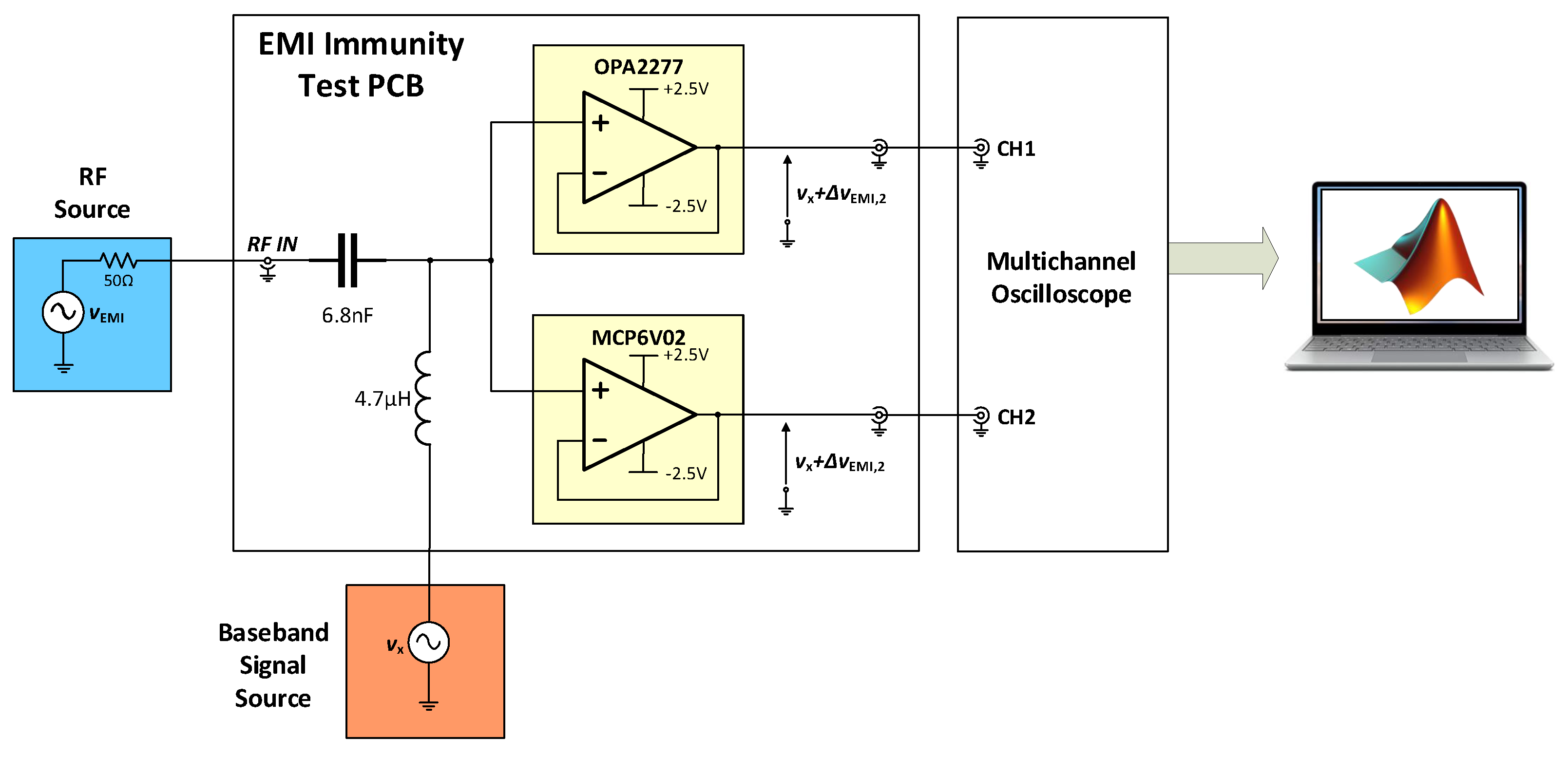
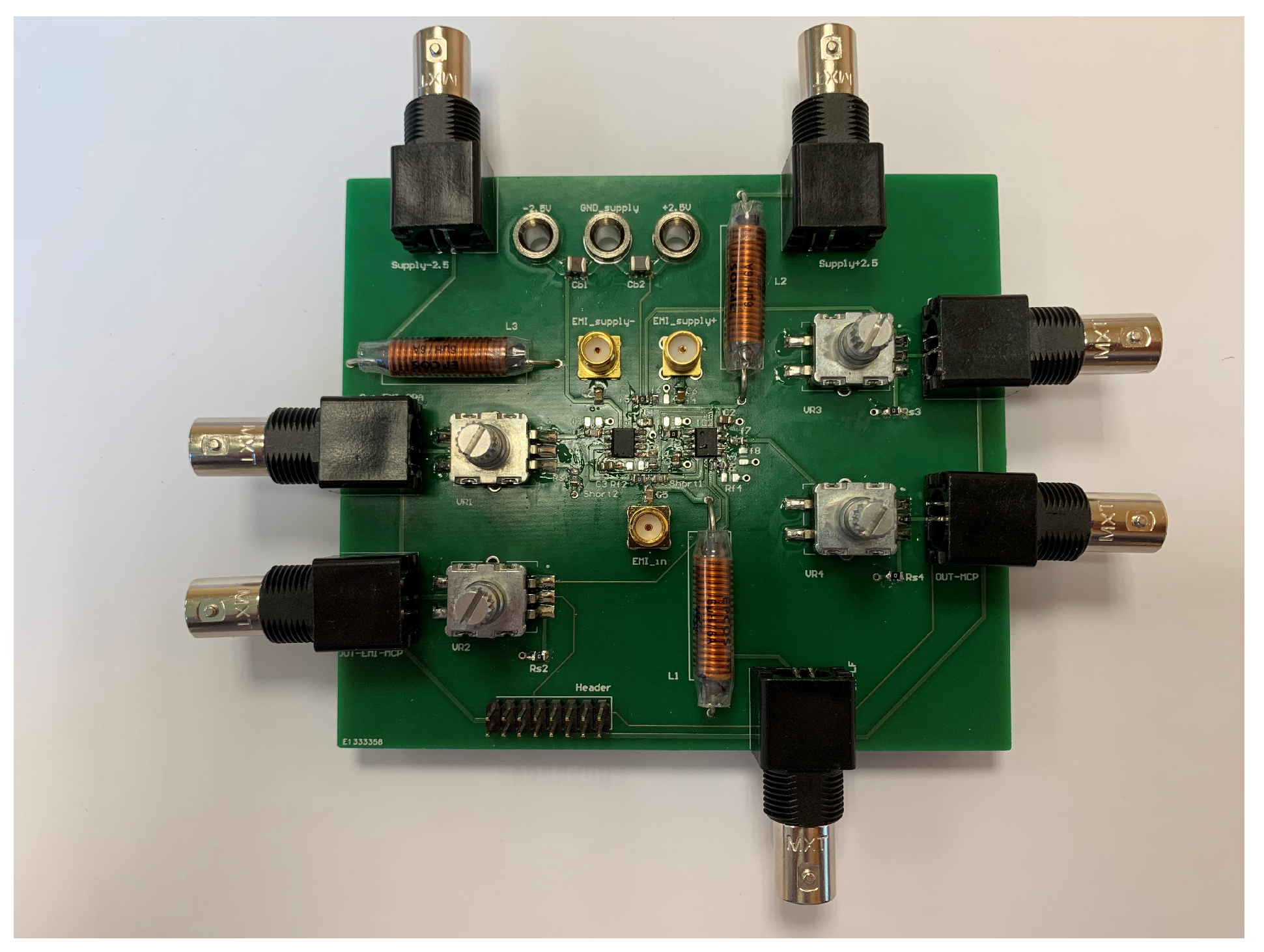
The block diagram of the fabricated test PCB is included in the test setup block diagram in Figure 3, whereas its photograph is shown in Figure 4. In such a test board, an RF signal, provided by an RF source connected to the PCB via an SMA connector, is superimposed to a low frequency input signal by an L C summing network (Bias Tee), which includes a ceramic capacitor of 6.8 nF and an inductor of 6 μ H , designed in compliance with the DPI standard requirements [48]. The same L C network also serves as a low-pass anti-aliasing filter for the low-frequency input.
Following the block diagram in Figure 2, the output node of the L C summing network is connected through microstrip traces with less than 1cm length and with 100 Ω characteristic impedance to the inputs of the two conditioning amplifiers, which are implemented by two different precision opamp circuits available in commerce, i.e., the OPA2277 opamp by Texas Instruments [50] and the MCP6V02 [51] by Microchip, whose main electrical characteristics taken from datasheets are reported in Table 1, and whose relevant susceptibility to EMI has been experimentally characterized in previous literature [52], revealing opposite EMI induced offset voltage under continuous wave EMI excitation.
Both the opamps are connected in the voltage follower configuration and are operated at a positive power supply voltage of +2.5 V and at a negative supply voltage of −2.5 V with respect to the reference voltage of the input signal (0 V). The opamp supply voltages are locally decoupled by 100 nF capacitors. The output terminals of the conditioning amplifiers in the PCB boards are fed to two BNC connectors so that to be transferred to an external digitizer and digital signal processor.

3.2. Experimental Test Setup

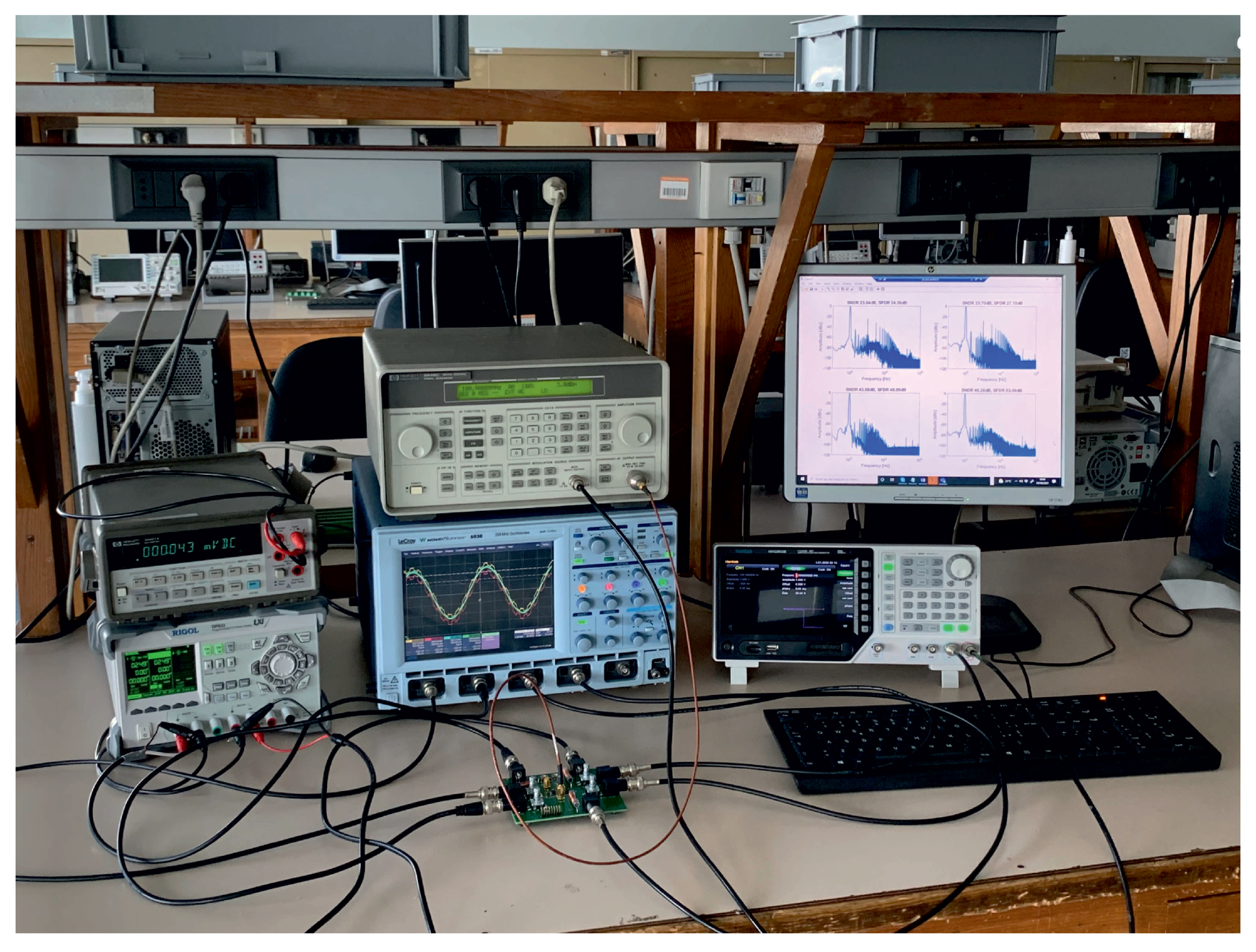
In order to test the proposed EMI-robust AFE, the nominal input of the EMI test PCB described above has been connected to a low frequency waveform generator Hantek HDG2032B, while its SMA connector has been connected to an RF signal source HP 8648C, which is suitable to generate a continuous-wave or modulated RF signal in the 1 MHz–3.2 GHz bandwidth with an output incident power up to 20 dBm for EMI injection, as shown in Figure 5. In the same setup, the outputs of the conditioning amplifiers have been connected to a LeCroy Waverunner 6030 multichannel oscilloscope to be digitized and made available to a PC, in which the EMI suppression strategy discussed in Section 2.3 is implemented in the Matlab environment.

4. Experimental Results

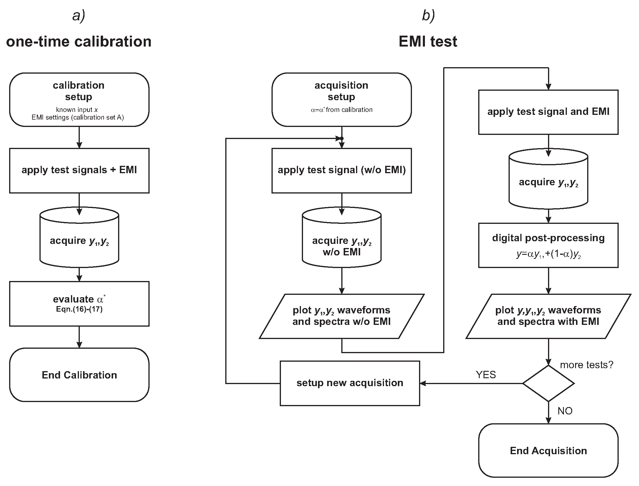
In order to validate the proposed AFE with digital-based EMI induced error cancellation and to discuss its effectiveness and versatility under different application scenarios, the EMI test PCB has been initially calibrated as discussed in Section 2.4 and illustrated in Figure 6a to get the optimal EMI suppression coefficient, which was found to be α * = 0.445 for the opamps considered in this test. Then, the AFE has been extensively tested under a variety of test conditions, namely:
  • zero nominal input and CW EMI;
  • low frequency (100 Hz) sinewave nominal input and AM EMI, with square-wave, sine-wave and exponential modulating signals;
For each of test condition, the AFE has been tested according to the procedure illustrated in the flow chart of Figure 6b. In particular, the waveforms retrieved by the proposed procedure (y in Equation (10)) are compared with those obtained by direct digitizing of the OPA2277 and of the MCP6V02 opamps output voltages corrupted by EMI ( y 1 and y 2 in Equation (8) and Equation (9), and by the output y 1 and y 2 obtained under the same conditions without EMI injection.

4.1. Tests under CW EMI Excitation

The AFE described before has been initially tested with a 0 V nominal DC input and with CW EMI excitation with 100 MHz frequency and incident power ranging from 15 dBm to +   9 dBm , corresponding to an EMI peak amplitude ranging from V emi , pk = 112 mV to V emi , pk = 1.78 V (Figure 7a,c), and with CW EMI excitation with 0 dBm incident power ( V emi , pk = 632 mV ) and frequency ranging from 50 MHz to 500 MHz (Figure 7b,d), so that to characterize the OPA2277 and the MCP6V02 opamp circuits included in the fabricated EMI test board and the whole AFE with digital EMI suppression in terms of the parameters which are commonly adopted to quantify the susceptibility to EMI of opamp circuits, i.e., the EMI-induced input offset voltage Δ V OFF [21] (Figure 7a,b), and the EMI Rejection Ratio (EMIRR) [52] (Figure 7c,d), defined as:
EMIRR = 20 log 10 V emi , pk 2 Δ V OFF · 100 mV
The experimental results, reported in Figure 7, reveal that the waveform retrieved from the proposed AFE shows an EMI induced offset of less than 2.6 mV ( 3.2 mV ) over the considered EMI amplitude (frequency) range, corresponding to an EMIRR above 60 dB at 100 MHz EMI frequency and above 85 dB for EMI exceeding 200 MHz . Under the same test conditions, the OPA2277 (MCP6V02) opamp shows a relevant positive (negative) offset voltage up to more than 200 mV , corresponding to an EMIRR below 40 dB at 100 MHz and of about 52 dB at 200 MHz .
Comparing the intrinsic EMIRR of the opamps with and without the proposed approach, it can be observed that the proposed solution results in an improvement ranging from 20 dB to 40 dB for EMI frequencies below 200 MHz , which is expectedly reduced above 300 MHz , where the intrinsic EMIRR of the two opamps is higher and their EMI-induced offset voltage is already below 1 mV and compared with the measurement uncertainty and with the quantization error.
These results confirm the effectiveness of the proposed approach, and an EMI immunity outperforming previously commercial EMI hardened opamps [53] and EMI-robust opamp circuits proposed in the literature [26,27,28,29,30,31,32,33,34,35,36,37,38,39,40,41,42], which require custom analog ICs and a significant design effort.

4.2. Low Frequency Sinewave Nominal Input and AM EMI Excitation

While the EMI susceptibility characterization in previous literature is mostly limited to the evaluation of the EMI induced offset voltage and/or of the EMIRR under a 0 V DC input as discussed above, an extensive experimental characterization of the proposed AFE in the presence of a non-constant baseband input and under modulated EMI excitation is offered in this paper to challenge the robustness of the simple EMI cancellation method described in Section 2.3 and to thoroughly describe the quality of the acquired signal and its EMI-induced degradation.
For this purpose, the AFE has been first tested without EMI excitation, with a nominal sinewave input at 100 Hz frequency and 500 mV peak amplitude, which has been acquired directly at the signal generator output over a time interval of 200 ms at a sample rate of 5 MS / s by the oscilloscope with a 256 averaging factor and is reported in Figure 8a. The spectrum of the signal (excluding its DC component) is then calculated using a Blackman window and is reported in Figure 8b in the frequency range 0–1 MHz , corresponding to the opamps bandwidth. With reference to the spectrum, the signal-to-noise and distortion ratio (SNDR) and the spurious free dynamic range (SFDR) are reported as a benchmark of the acquired signal quality. The SNDR is evaluated as:
S N D R = 10 log 10 P sin P total P sin
where P sin is the power of the nominal sinewave input, i.e., V sin 2 / 2 , where V sin is the peak amplitude of the sinewave, and P total is the total power v x 2 ¯ of the acquired signal, whereas the SFDR is evaluated as:
S F D R = 10 log 10 P sin P max , spur
where P max , spur is the power level of the highest spurious spectral component, including the harmonics of the nominal signal.
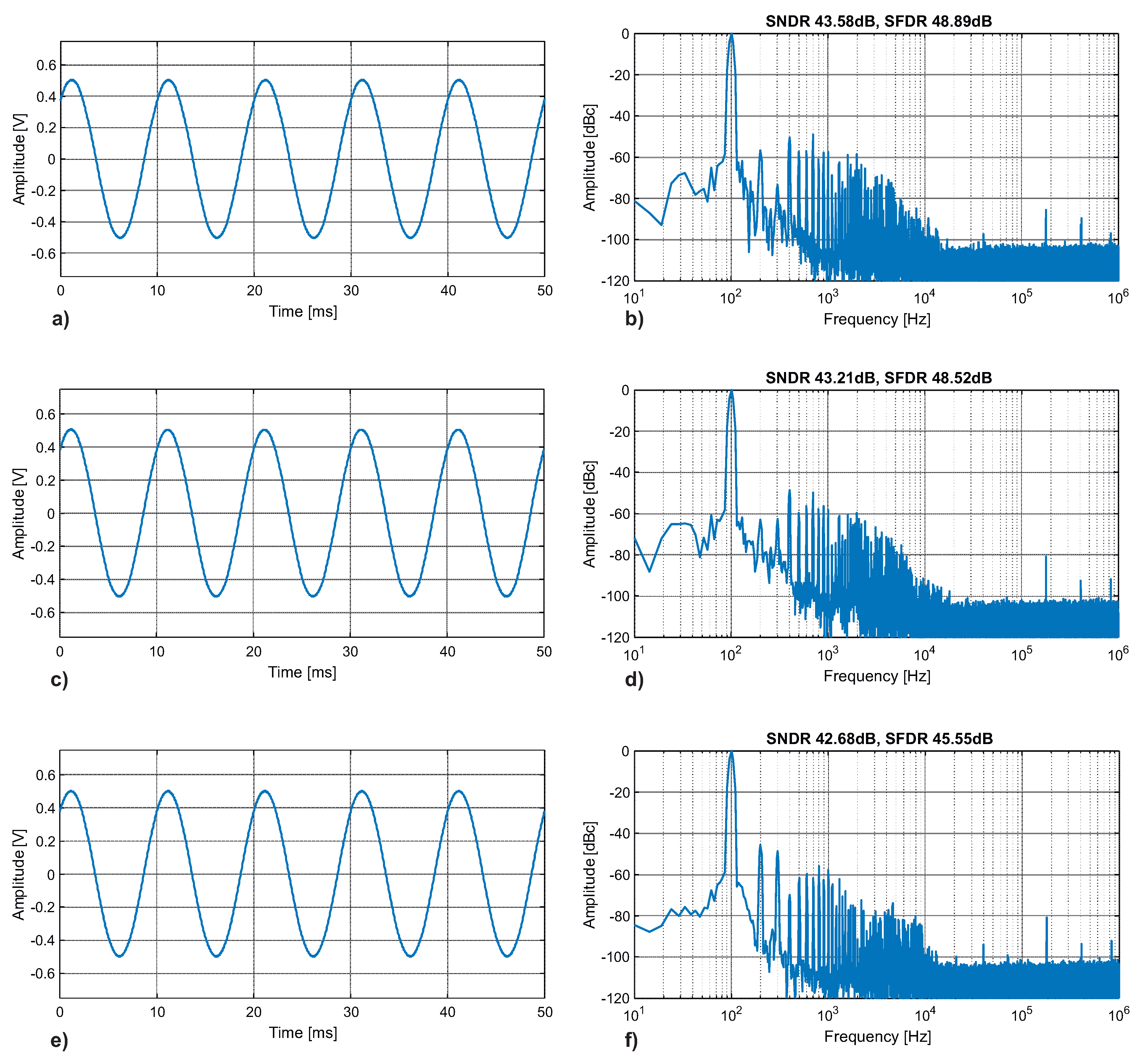
The output voltages of the two opamps with no EMI excitation have been also acquired as described above and are reported in Figure 8c–f. Looking at Figure 8, it can be observed that the SNDR (SFDR) are intrinsically limited to 43.58 dB (48.89 dB) by the waveform generator and by the ADC in the oscilloscope, while, comparing Figure 8b and Figure 8d,f, the limitations of the opamps result in a slight degradation in the SNDR (SFDR) of less than 1 dB (3.5 dB) in the worst case (It is worth observing that the OPA2277 second and third harmonic distortions in our setup, in which the opamp is powered at ± 2.5 V, is significantly worse than what reported in the datasheet under ± 15 V power supply voltage.).
In order to test the EMI-induced degradation in the acquired signals with and without the proposed EMI error suppression strategy, the same PCB has then been tested under the same nominal signal, superimposing an AM modulated EMI waveform
v EMI , AM = V emi , pk 1 + m · v mod ( t ) V mod , pk sin 2 π f 0 t
where V emi , pk is the open-circuit EMI carrier peak amplitude, expressed in terms of the EMI incident test power P inc as:
V emi , pk = 2 2 · P inc · 50 Ω ,
0 < m 1 is the modulation index, v mod ( t ) is the modulating waveform, V mod , pk = 1 V and f 0 is the carrier frequency.
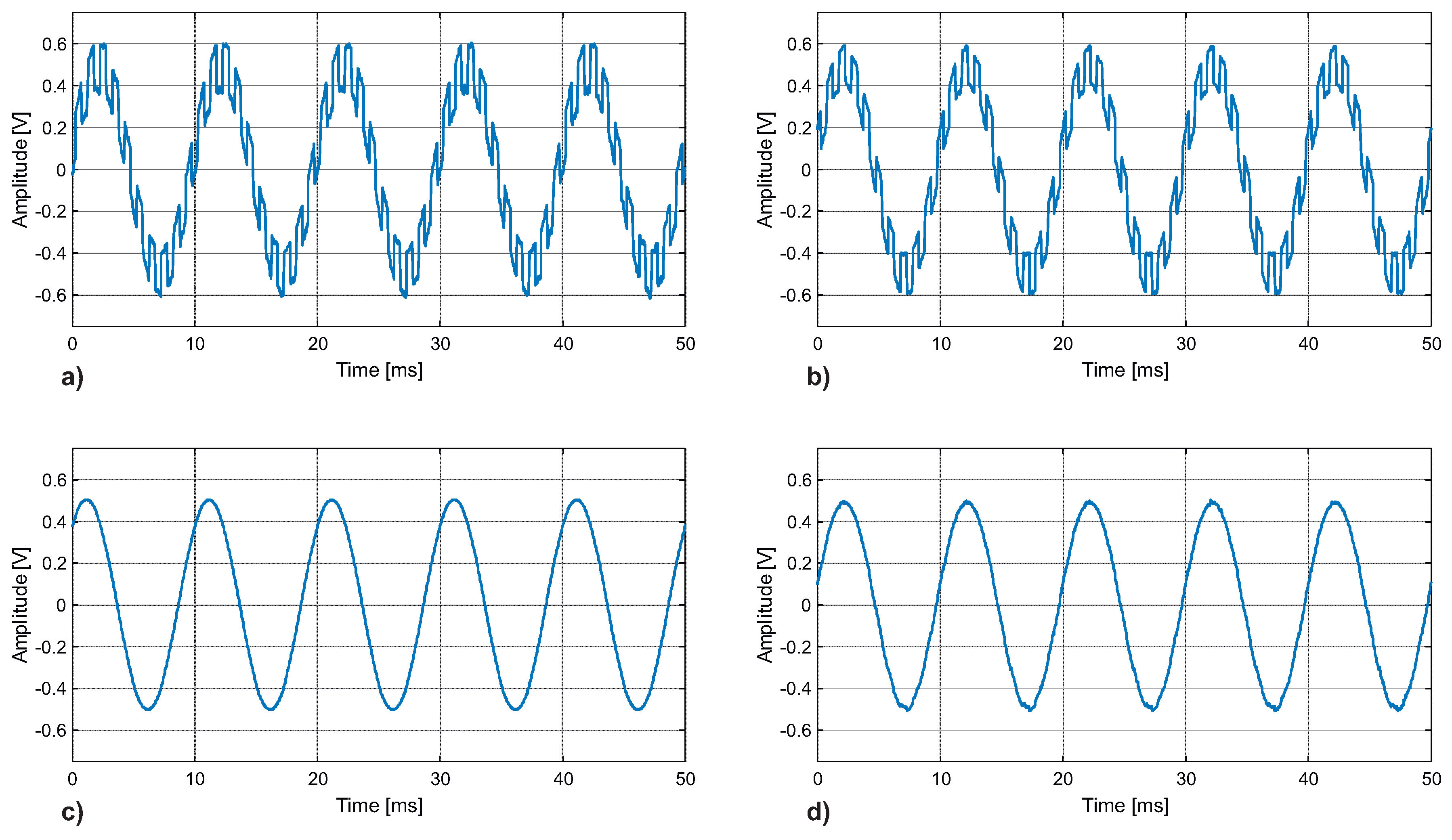
The raw opamp output waveforms measured for f 0 = 100 MHz , P inc = 0 dBm , corresponding to a carrier peak amplitude V emi , pk = 632 mV , and for a 0 1 V , 50 % duty cycle, 1 kHz frequency square wave modulating signal v mod ( t ) with m = 100 % modulation index are reported in Figure 9a,b reveal, as expected [4,21], a significant degradation due to the presence of a large EMI-induced error proportional to the modulating signal added to the nominal signal. At the same time, the waveform retrieved based on the data in Figure 9a,b by the proposed digital EMI-induced error suppression technique is reported in Figure 9d and is very similar to the uncorrupted nominal signal, reported in Figure 9c for comparison.
The substantial improvement is confirmed by the spectra in Figure 10. Here, EMI-induced spurs at the harmonics of the 1 kHz modulating frequency can be observed in the individual opamp output signals (Figure 10a,b), whose SNDR (SFDR) are severely degraded to 23.04 dB ( 24.38 dB ) in the worst case. Such EMI-induced spurs, however, are effectively suppressed by the proposed approach (Figure 10d) resulting in an SNDR (SFDR) of 46.26 dB ( 53.09 dB ), which are even higher than for the original signal (Figure 10c), i.e., 43.58 dB ( 48.89 dB ). The higher SNDR can be explained considering that the proposed approach results in averaging of uncorrelated quantization and thermal noise components over two acquisitions, whereas a partial compensation of the different baseband distortion components motivates the better SFDR.
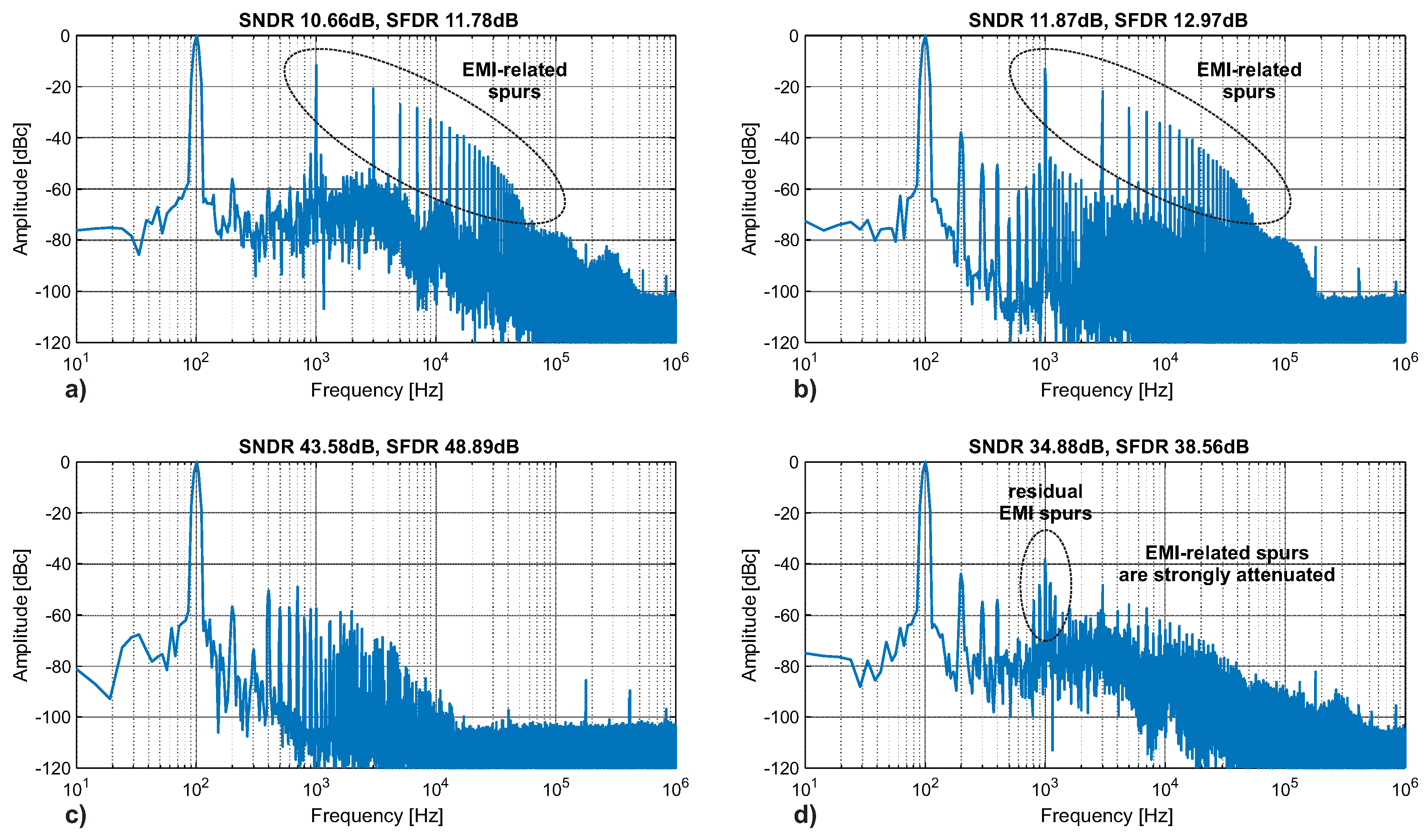
The results of the same tests in Figure 9 and Figure 10 are reported in Figure 11 and Figure 12 for an increased EMI incident power of 9 dBm , corresponding to a 1.783 V peak amplitude, comparable with the rail-to-rail power supply swing of the two opamps. Such a very high EMI amplitude leads to severely corrupted time-domain opamp output waveforms (Figure 11a,b), corresponding to a measured SNDR (SFDR) just above 10 dB . In spite of the severe EMI excitation, the proposed approach leads to a barely visible distortion in the lower part of the output waveform (Figure 11d) which corresponds to a measured SNDR (SFDR) of 34.88 dB ( 38.56 dB ), which are 23 dB ( 25 dB ) better than the raw opamp output waveforms, even if degraded of about 10 dB compared to the original signal (Figure 12c). The residual error can be related to higher order distortion not captured by the model in (5) and (6) and in the derivation of the proposed approach.
In Figure 13, the SNDR and SFDR measured under AM modulated square wave injection as in Figure 10 and Figure 12 are plotted for the raw opamp output waveforms and for the waveform obtained by the proposed post-processing under different EMI incident power ranging from 15 dBm ( 112 mV peak) up to 9 dBm ( 1.78 V peak) in Figure 13a,b. The same test has been repeated for a sinewave modulating waveform, i.e., for:
v mod ( t ) = V mod , pk sin 2 π f m t
with f m = 1 kHz in (23), and the measured SNDR and SFDR are reported in Figure 13c,d. All the results reported in Figure 13 confirm the substantial effectiveness of the proposed compensation approach with the same EMI compensation coefficient α = 0.445 both under small and large signal EMI excitation and regardless of the modulating waveform.
To further verify the robustness of the proposed approach with the same compensation coefficient, the test has been repeated with 0 dBm incident power over different carrier frequencies f 0 ranging from 50 MHz up to 500 MHz and for AM modulation indexes m ranging from 25% to 100%. The measured SNDR and SFDR obtained in these tests are reported in Figure 14 and confirm the effectiveness and the robustness of the approach over a wide variety of EMI excitation conditions.
Moreover, the measured waveforms and spectra for P inc = 3 dBm , f 0 = 100 MHz and m = 100 % modulation index under a damped exponential modulating signal, i.e., for
v mod ( t ) = V mod , pk h = + e t h T τ Π 1 t h T
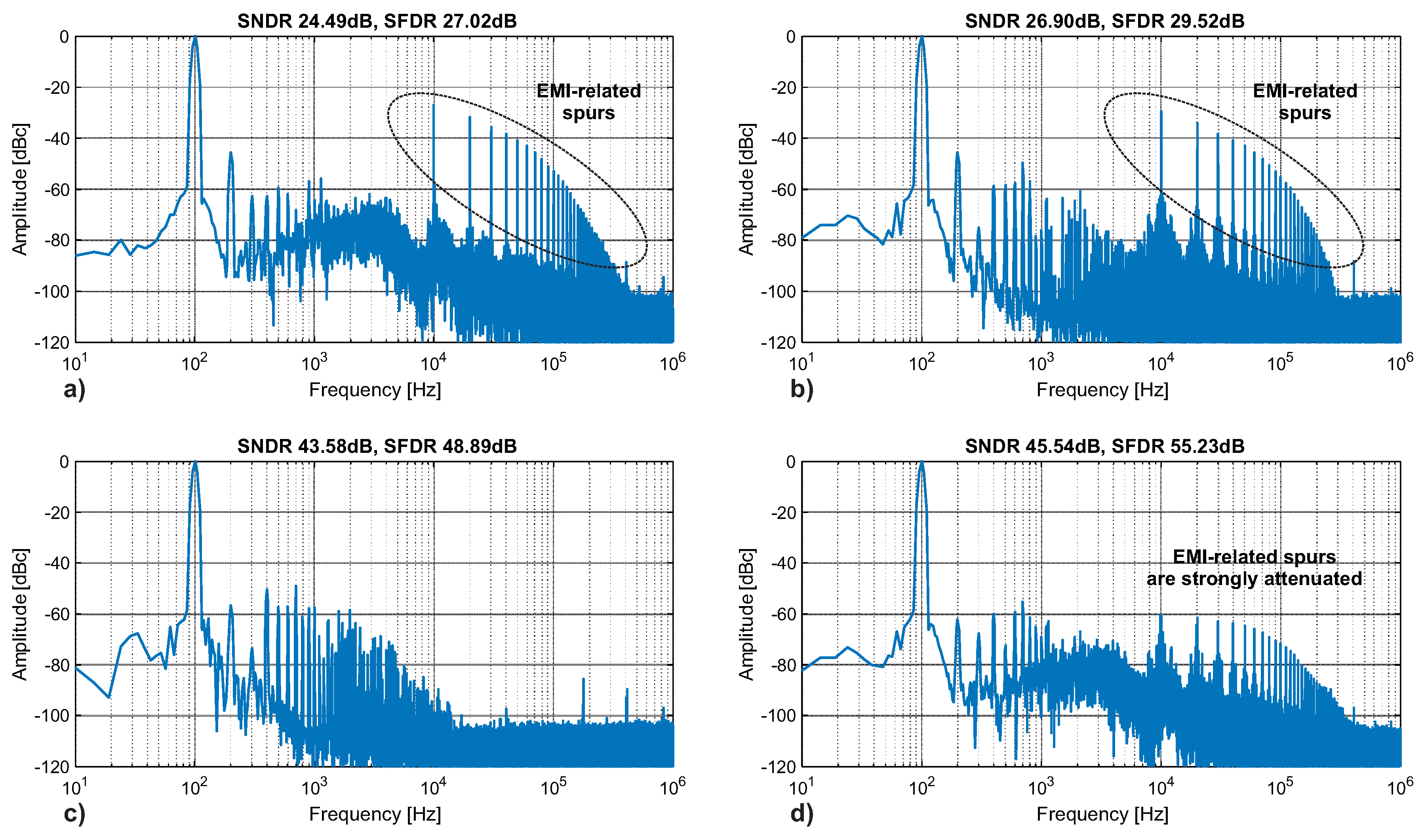
where Π ( x ) is the unit pulse function, which is 1 for 0 < x < 1 and zero elsewhere, with T = 0.1 ms , which could possibly describe the underdamped resonant waveforms resulting from the switching activity of digital circuits and power converters unintentionally superimposed to the input signal, have been acquired and reported in Figure 15 and Figure 16. The almost complete suppression of EMI-related spurs at the harmonics of 10 kHz , which are clearly visible in the raw opamp output voltages (Figure 16a,b) can be clearly observed in Figure 16c and further validates the proposed approach.

5. Conclusions

The possibility to correct EMI-induced errors in baseband AFE by digital post-processing has beed thoroughly investigated. In particular, it has been shown how the dominant EMI-induced errors related to EMI rectification in opamp-based conditioning amplifiers can be compensated in the digital domain by a very simple weighted sum post-processing, starting from acquisitions of EMI-corrupted signals conditioned by opamp-based amplifiers with similar baseband characteristics but with a different susceptibility to EMI.
The proposed approach has been experimentally verified for the first time with reference to a specifically designed EMI test PCB suitable to perform DPI EMC tests on an AFE including two different off-the-shelf opamp circuits in the voltage follower configuration. Extensive testing under CW and AM modulated EMI at different amplitude, frequency, modulation index and modulation profile reveals the effectiveness and the robustness of the proposed approach.
The results presented in this paper confirm the effectiveness of the idea suggested in [47] and reveal how a superior degree of immunity to EMI can be achieved in AFEs based on standard off-the-shelf opamps just by simple digital processing, without requiring expensive and possibly impractical ad hoc EMI-hardened analog hardware.
The research paves the way to a new generation of low-cost, EMI hardened sensor readouts targeting specific applications in the automotive, smart grid, IoT and biomedical fields. Moreover, taking advantage of digital processing, the proposed approach enables the integration on silicon of digital-based EMI-hardened AFEs in nanoscale technologies suitable to operate at ultra-low supply voltage and ultra-low power consumption. The application of the proposed approach in the design of specific sensor readout, both at system and integrated circuit level, will be explored in future work.

Author Contributions

Conceptualization, P.C.; methodology, P.C.; test PCB design and fabrication: F.M.; validation, F.M. and P.C; formal analysis, P.C.; investigation, P.C.; resources, P.C. and F.M.; writing—original draft preparation, P.C.; writing—review and editing, F.M.; supervision, P.C. All authors have read and agreed to the published version of the manuscript.

Funding

This research received no external funding.

Acknowledgments

The authors acknowledge the support of Gianfranco Albis in setting up the experimental test bench.

Conflicts of Interest

The authors declare no conflict of interest.

References

  1. Dhia, S.B.; Ramdani, M.E.S. Electromagnetic Compatibility of Integrated Circuits: Techniques for Low Emission and Susceptibility, 1st ed.; Springer: Berlin/Heidelberg, Germany, 2006. [Google Scholar]
  2. Redouté, J.-M.; Steyaert, M. EMC of Analog Integrated Circuits; Springer: Berlin/Heidelberg, Germany, 2010. [Google Scholar]
  3. Totev, E.D. Out-of-Band Interference Immunity of Negative-Feedback Amplifiers. Ph.D. Thesis, TU Delft, Delft, The Netherlands, 2021. [Google Scholar]
  4. Gago, J.; Balcells, J.; GonzÁlez, D.; Lamich, M.; Mon, J.; Santolaria, A. EMI Susceptibility Model of Signal Conditioning Circuits Based on Operational Amplifiers. IEEE Trans. Electromagn. Compat. 2007, 49, 849–859. [Google Scholar] [CrossRef]
  5. Zhang, Y.; Rasmussen, K. Detection of electromagnetic interference attacks on sensor systems. In Proceedings of the 2020 IEEE Symposium on Security and Privacy, San Francisco, CA, USA, 18–21 May 2020; pp. 203–216. [Google Scholar] [CrossRef]
  6. Aiello, O.; Crovetti, P.S.; Fiori, F. Susceptibility to EMI of a Battery Management System IC for electric vehicles. In Proceedings of the 2015 IEEE International Symposium on Electromagnetic Compatibility (EMC), Dresden, Germany, 16–22 August 2015; pp. 749–754. [Google Scholar] [CrossRef]
  7. Maouloud, A.; Klingler, M.; Besnier, P. A Test Setup to Assess the Impact of EMI Produced by On-Board Electronics on the Quality of Radio Reception in Vehicles. IEEE Trans. Electromagn. Compat. 2021. [Google Scholar] [CrossRef]
  8. Sacco, E.; Vergauwen, J.; Gielen, G. Improving the EMI Robustness of Feedback-based Time-Encoding Readout Architectures for Resistive Sensor Interfaces. In Proceedings of the 2020 27th IEEE International Conference on Electronics, Circuits and Systems (ICECS), Glasgow, UK, 23–25 November 2020; pp. 1–4. [Google Scholar] [CrossRef]
  9. Bassen, H.; Mendoza, G. Comparison of injected and radiated EMC testing of active implanted cardiac medical devices at the boundary frequency of 450 MHz. IEEE Electromagn. Compat. Mag. 2016, 5, 64–70. [Google Scholar] [CrossRef] [Green Version]
  10. Aiello, O.; Crovetti, P.; Fiori, F. Investigation on the susceptibility of hall-effect current sensors to EMI. In Proceedings of the 10th International Symposium on Electromagnetic Compatibility, York, UK, 26–30 September 2011; pp. 368–372. [Google Scholar]
  11. Shoaib, N.; Zaidi, S.N.F.; Shafqat, A.; Cheema, H.M. EMC/I Analysis of Miniaturized Bio-Mechanical Sports Wearables. In Proceedings of the 2019 12th International Workshop on the Electromagnetic Compatibility of Integrated Circuits (EMC Compo), Hangzhou, China, 21–23 October 2019; pp. 210–212. [Google Scholar] [CrossRef]
  12. Have, B.T.; Azpúrua, M.A.; Hartman, T.; Pous, M.; Moonen, N.; Silva, F.; Leferink, F. Estimation of Static Energy Meter Interference in Waveforms Obtained in On-Site Scenarios. IEEE Trans. Electromagn. Compat. 2021, 1–8. [Google Scholar] [CrossRef]
  13. Wu, J.; Qi, Y.; Gong, G.; Fan, J.; Miao, M.; Yu, W.; Ma, J.; Drewniak, J.L. Review of the EMC Aspects of Internet of Things. IEEE Trans. Electromagn. Compat. 2020, 62, 2604–2612. [Google Scholar] [CrossRef]
  14. Crovetti, P.; Fiori, F. Efficient BEM-based substrate network extraction in silicon SoCs. Microelectron. J. 2008, 39, 1774–1784. [Google Scholar] [CrossRef]
  15. Crovetti, P.S.; Fiori, F. Distributed conversion of common-mode into differential-mode interference. IEEE Trans. Microw. Theory Tech. 2011, 59, 2140–2150. [Google Scholar] [CrossRef]
  16. Musolino, F.; Crovetti, P.S. Interference of Spread-Spectrum Modulated Disturbances on Digital Communication Channels. IEEE Access 2019, 7, 158969–158980. [Google Scholar] [CrossRef]
  17. Crovetti, P.S.; Musolino, F.; Aiello, O.; Toledo, P.; Rubino, R. breaking the boundaries between analogue and digital. Electron. Lett. 2019, 55, 672–673. [Google Scholar] [CrossRef]
  18. Crovetti, P.S.; Musolino, F. Interference of Spread-Spectrum EMI and Digital Data Links under Narrowband Resonant Coupling. Electronics 2020, 9, 60. [Google Scholar] [CrossRef] [Green Version]
  19. Graffi, S.; Masetti, G.; Golzio, D. New macromodels and measurements for the analysis of EMI effects in 741 op-amp circuits. IEEE Trans. Electromagn. Compat. 1991, 33, 25–34. [Google Scholar] [CrossRef]
  20. Kovacs-Vajna, Z.; Sardini, E.; Speciale, N. Chaotic behavior of 741 opamps subjected to EMI conveyed to power supply rails. In Proceedings of the 2000 IEEE International Symposium on Circuits and Systems (ISCAS), Geneva, Switzerland, 28–31 May 2000; Volume 1, pp. 727–730. [Google Scholar] [CrossRef]
  21. Fiori, F.; Crovetti, P. Nonlinear effects of radio-frequency interference in operational amplifiers. IEEE Trans. Circuits Syst. I Fundam. Theory Appl. 2002, 49, 367–372. [Google Scholar] [CrossRef]
  22. Fiori, F. A new nonlinear model of EMI-induced distortion phenomena in feedback CMOS operational amplifiers. IEEE Trans. Electromagn. Compat. 2002, 44, 495–502. [Google Scholar] [CrossRef]
  23. Abuelma’atti, M. Analysis of the effect of radio frequency interference on the DC performance of bipolar operational amplifiers. IEEE Trans. Electromagn. Compat. 2003, 45, 453–458. [Google Scholar] [CrossRef]
  24. Fiori, F.; Crovetti, P. Prediction of high-power EMI effects in CMOS operational amplifiers. IEEE Trans. Electromagn. Compat. 2006, 48, 153–160. [Google Scholar] [CrossRef]
  25. Crovetti, P.S. Finite Common-Mode Rejection in Fully Differential Nonlinear Circuits. IEEE Trans. Circuits Syst. II Express Briefs 2011, 58, 507–511. [Google Scholar] [CrossRef]
  26. Richelli, A.; Delaini, G.; Grassi, M.; Redouté, J.M. Susceptibility of Operational Amplifiers to Conducted EMI Injected Through the Ground Plane into Their Output Terminal. IEEE Trans. Reliab. 2016, 65, 1369–1379. [Google Scholar] [CrossRef]
  27. Zupan, D.; Deutschmann, B. Comparison of EMI Improved Differential Input Pair Structures Within an Integrated Folded Cascode Operational Transconductance Amplifier. In Proceedings of the 2020 Austrochip Workshop on Microelectronics (Austrochip), Vienna, Austria, 7 October 2020; pp. 47–52. [Google Scholar] [CrossRef]
  28. Gundla, J.; Boyapati, S.; Pasupureddi, V.S.R. Compact CMOS Miller OpAmp With High EMI-Immunity. IEEE Trans. Electromagn. Compat. 2020, 62, 2394–2400. [Google Scholar] [CrossRef]
  29. Lavarda, A.; Petruzzi, L.; Radež, N.; Deutschmann, B. On the Robustness of CMOS-Chopped Operational Amplifiers to Conducted Electromagnetic Interferences. IEEE Trans. Electromagn. Compat. 2018, 60, 478–486. [Google Scholar] [CrossRef]
  30. Becchetti, S.; Richelli, A.; Colalongo, L.; Kovacs-Vajna, Z. A Comprehensive Comparison of EMI Immunity in CMOS Amplifier Topologies. Electronics 2019, 8, 1181. [Google Scholar] [CrossRef] [Green Version]
  31. Pudi N.S., A.K.; Redouté, J.M.; Baghini, M.S. A Generic EMI-Immune Technique for Differential Amplifiers With Single-Ended Output. IEEE Trans. Electromagn. Compat. 2018, 60, 958–964. [Google Scholar] [CrossRef]
  32. Richelli, A.; Kennedy, S.; Redouté, J.M. An EMI-Resistant Common-Mode Cancelation Differential Input Stage in UMC 180 nm CMOS. IEEE Trans. Electromagn. Compat. 2017, 59, 2049–2051. [Google Scholar] [CrossRef]
  33. Boyapati, S.; Redouté, J.M.; Baghini, M.S. Modeling and design of an EMI-immune source-buffered Miller OpAmp in 0.18-μm CMOS technology. In Proceedings of the 2017 International Symposium on Electromagnetic Compatibility—EMC EUROPE, Angers, France, 4–7 September 2017; pp. 1–5. [Google Scholar] [CrossRef]
  34. Boyapati, S.; Redouté, J.M.; Shojaei Baghini, M. Design of A Novel Highly EMI-Immune CMOS Miller OpAmp Considering Channel Length Modulation. IEEE Trans. Circuits Syst. I Regul. Pap. 2017, 64, 2679–2690. [Google Scholar] [CrossRef]
  35. Boyapati, S.; Redouté, J.M.; Baghini, M.S. Modeling and Design of EMI-Immune OpAmps in 0.18-μm CMOS Technology. IEEE Trans. Electromagn. Compat. 2016, 58, 1609–1616. [Google Scholar] [CrossRef]
  36. Fiori, F. On the Susceptibility of Chopper Operational Amplifiers to EMI. IEEE Trans. Electromagn. Compat. 2016, 58, 1000–1006. [Google Scholar] [CrossRef]
  37. Richelli, A.; Matig-A, G.; Redouté, J.M. Design of a folded cascode opamp with increased immunity to conducted electromagnetic interference in 0.18 μm CMOS. Microelectron. Reliab. 2015, 55, 654–661. [Google Scholar] [CrossRef]
  38. Redouté, J.M.; Richelli, A. A methodological approach to EMI resistant analog integrated circuit design. IEEE Electromagn. Compat. Mag. 2015, 4, 92–100. [Google Scholar] [CrossRef] [Green Version]
  39. Yu, J.; Amer, A.; Sanchez-Sinencio, E. Electromagnetic Interference Resisting Operational Amplifier. IEEE Trans. Circuits Syst. I Regul. Pap. 2014, 61, 1917–1927. [Google Scholar] [CrossRef]
  40. Richelli, A. Increasing EMI Immunity in Novel Low-Voltage CMOS OpAmps. IEEE Trans. Electromagn. Compat. 2012, 54, 947–950. [Google Scholar] [CrossRef] [Green Version]
  41. Richelli, A. CMOS OpAmp Resisting to Large Electromagnetic Interferences. IEEE Trans. Electromagn. Compat. 2010, 52, 1062–1065. [Google Scholar] [CrossRef] [Green Version]
  42. Crovetti, P. Operational amplifier immune to EMI with no baseband performance degradation. Electron. Lett. 2010, 46, 207–208. [Google Scholar] [CrossRef]
  43. Walravens, C.; Van Winckel, S.; Redoute, J.M.; Steyaert, M. Efficient reduction of electromagnetic interference effects in operational amplifier. Electron. Lett. 2007, 4, 84–85. [Google Scholar] [CrossRef]
  44. Fiori, F.; Crovetti, P. Complementary differential pair with high immunity to RFI. Electron. Lett. 2002, 38, 1663–1664. [Google Scholar] [CrossRef]
  45. Crovetti, P.S. A Digital-Based Analog Differential Circuit. IEEE Trans. Circuits Syst. I Reg. Pap. 2013, 60, 3107–3116. [Google Scholar] [CrossRef]
  46. Crovetti, P.S. A Digital-Based Virtual Voltage Reference. IEEE Trans. Circuits Syst. I Regul. Pap. 2015, 62, 1315–1324. [Google Scholar] [CrossRef]
  47. Crovetti, P. Acquisition front-end immune to EMI. Electron. Lett. 2012, 48, 1114–1115. [Google Scholar] [CrossRef]
  48. Integrated Circuits, Measurement of Electromagnetic Immunity, 150 kHz–1 GHz, IEC Standard, IEC62132; Technical Report; International Electrotechnical Commission (IEC): Geneva, Switzerland, 2006.
  49. Kashinath, S.A.; Mostafa, S.A.; Mustapha, A.; Mahdin, H.; Lim, D.; Mahmoud, M.A.; Mohammed, M.A.; Al-Rimy, B.A.S.; Fudzee, M.F.M.; Yang, T.J. Review of Data Fusion Methods for Real-Time and Multi-Sensor Traffic Flow Analysis. IEEE Access 2021, 9, 51258–51276. [Google Scholar] [CrossRef]
  50. OPAx277 High Precision Operational Amplifiers; Technical Report; Texas Instruments: Dallas, TX, USA, 2015.
  51. MCP6V01/2/3 300 μA, Auto-Zeroed Op Amps; Technical Report; Microchip Technologies Inc.: Chandler, AZ, USA, 2008.
  52. Aimonetto, M.B.; Fiori, F. On the effectiveness of EMIRR to qualify OpAmps. In Proceedings of the 2015 IEEE International Symposium on Electromagnetic Compatibility (EMC), Dresden, Germany, 16–22 August 2015; pp. 40–44. [Google Scholar] [CrossRef]
  53. LMV861 Single 30 MHz Low Power CMOS, EMI Hardened Operational Amplifiers, Rev. C; Technical Report; Texas Instruments: Dallas, TX, USA, 2013.
Figure 1. Acquisition Front-End Architecture.
Electronics 10 02096 g001
Figure 2. New Acquisition Front-End Architecture aimed to compensate EMI-induced distortions due to EMI rectification by digital processing.
Electronics 10 02096 g002
Figure 3. Acquisition Front-End Test Bench block diagram, with detail of the fabricated EMI test PCB.
Electronics 10 02096 g003
Figure 4. Photograph of the fabricated EMI test PCB.
Electronics 10 02096 g004
Figure 5. Photograph of the experimental test bench.
Electronics 10 02096 g005
Figure 6. Flow chart of the calibration procedure (a) and of the EMI test procedure (b) adopted to test the susceptibility of the proposed AFE.
Electronics 10 02096 g006
Figure 7. EMI-Induced Input Offset Voltage and EMI Rejection Ratio (EMIRR) for the proposed AFE and for the OPA2277 and the MCP6V02 opamps under continuous wave (CW) EMI excitation: (a) EMI-induced offset vs. CW EMI amplitude for a constant EMI frequency of 100MHz, (b) EMI-induced offset vs. CW EMI frequency, for a constant EMI amplitude of 0dBm, (c) EMIRR vs. CW EMI amplitude for a constant EMI frequency of 100MHz, (d) EMIRR vs. CW EMI frequency, for a constant EMI amplitude of 0 dBm.
Electronics 10 02096 g007
Figure 8. Time-domain waveforms and spectra of the low-frequency input signal and of the opamp output voltages with no EMI injection: (a) input signal, time domain waveform; (b) spectrum of the input signal; (c) MCP6V02 opamp output voltage, time domain waveform; (d) spectrum of the MCP6V02 opamp output voltage; (e) OPA2277 opamp output voltage, time domain waveform; (f) spectrum of the OPA2277 opamp output voltage.
Electronics 10 02096 g008
Figure 9. Time-domain waveform of the acquired signals under 0 dBm AM EMI excitation: (a) OPA2277 opamp output voltage with EMI injection; (b) MCP6V02 opamp output voltage with EMI injection; (c) OPA2277 opamp output voltage without EMI injection; (d) Output voltage with EMI injection estimated starting from the EMI corrupted waveforms in (a,b), by the proposed EMI-induced errors suppression procedure with α = 0.445 .
Electronics 10 02096 g009
Figure 10. Spectra of the measured signals under 0 dBm AM EMI excitation reported in Figure 9: (a) OPA2277 opamp output voltage with EMI injection; (b) MCP6V02 opamp output voltage with EMI injection; (c) nominal input signal spectrum as in Figure 8b; (d) Output voltage with EMI injection estimated starting from the EMI corrupted waveforms in (a,b), by the proposed EMI-induced errors suppression procedure with α = 0.445 .
Electronics 10 02096 g010
Figure 11. Time-domain waveform of the acquired signals under 9 dBm AM EMI excitation: (a) OPA2277 opamp output voltage with EMI injection; (b) MCP6V02 opamp output voltage with EMI injection; (c) nominal input signal spectrum as in Figure 8b; (d) Output voltage with EMI injection estimated starting from the EMI corrupted waveforms in (a,b), by the proposed EMI-induced errors suppression procedure with α = 0.445 .
Electronics 10 02096 g011
Figure 12. Spectra of the measured signals under 9 dBm AM EMI excitation reported in Figure 9: (a) OPA2277 opamp output voltage with EMI injection; (b) MCP6V02 opamp output voltage with EMI injection; (c) nominal input signal spectrum as in Figure 8b; (d) Output voltage with EMI injection estimated starting from the EMI corrupted waveforms in (a,b), by the proposed EMI-induced errors suppression procedure with α = 0.445 .
Electronics 10 02096 g012
Figure 13. Measured SNDR and SFDR of the waveforms obtained by the proposed EMI suppression technique with α = 0.445 (blue line, * marker), at the MCP6V02 output (red line, x marker), at the OPA2277 output (yellow line, + marker) in the presence of AM modulated EMI with carrier frequency 100MHz, square wave and sine-wave modulating signal at 100% modulation index, for an EMI incident power ranging from −15 dBm up to 9 dBm: (a) SNDR vs. incident power for square wave AM; (b) SFDR vs. incident power for square wave AM; (c) SNDR vs. incident power for sine wave AM; (d) SFDR vs. incident power for sine wave AM.
Electronics 10 02096 g013
Figure 14. Measured SNDR and SFDR of the waveforms obtained by the proposed EMI suppression technique with α = 0.445 (blue line, * marker), at the MCP6V02 output (red line, x marker), at the OPA2277 output (yellow line, + marker) in the presence of AM modulated EMI with carrier frequency ranging from 50 MHz to 500 MHz, square wave modulating signal with modulation index rangin from 25% to 100%, for an EMI incident power of 0 dBm: (a) SNDR vs. carrier frequency; (b) SFDR vs. carrier frequency; (c) SNDR vs. modulation index; (d) SFDR vs. modulation index.
Electronics 10 02096 g014
Figure 15. Time-domain waveform of the acquired signals under a damped exponential modulated EMI: (a) OPA2277 opamp output voltage with EMI injection; (b) MCP6V02 opamp output voltage with EMI injection; (c) nominal input signal spectrum as in Figure 8b; (d) Output voltage with EMI injection estimated starting from the EMI corrupted waveforms in (a,b), by the proposed EMI-induced errors suppression procedure with α = 0.445 .
Electronics 10 02096 g015
Figure 16. Spectra of the acquired signals under a damped exponential modulated EMI in Figure 15: (a) OPA2277 opamp output voltage with EMI injection; (b) MCP6V02 opamp output voltage with EMI injection; (c) nominal input signal spectrum as in Figure 8b; (d) Output voltage with EMI injection estimated starting from the EMI corrupted waveforms in (a,b), by the proposed EMI-induced errors suppression procedure with α = 0.445 .
Electronics 10 02096 g016
Table 1. Main Electrical Characteristics of the Precision Opamps included in the EMI test PCB.
PerformanceUnitOPA2277MCP6V02
Power Supply VoltageV+2.5 V/−2.5 V+2.5 V/−2.5 V
Supply Current μ A 800300
DC gaindB134130
CMRRdB140130
PSRRdB130130
Input Offset Voltage (max.) μ V 102
Input Referred Noise (0.1 Hz–10 Hz) μ V pp 0.222.5
THD%0.0002N/A
Gain-Bandwidth ProductMHz11.3
Slew RateV/ μ s0.80.5
Publisher’s Note: MDPI stays neutral with regard to jurisdictional claims in published maps and institutional affiliations.