1. Introduction
Intense competition among companies to bring electronic devices in the first place has demanded the development of strategies to reduce time to market. The re-usability of IP cores and an automatic design methodology reduce significantly the duration of the design cycle of embedded systems [
1]. However, the need to deploy functional systems in a short time has sometimes led to serious security problems by presenting information leaks that could reveal confidential data. Two well-known examples are Spectre and Meltdown, which are vulnerabilities that affect modern microprocessors. Spectre is a vulnerability that uses side-channel timing attacks to extract private data based on speculative execution resulting from a branch miss-prediction [
2]. Meltdown is related to a micro-architectural attack that exploits out-of-order execution to reveal the contents of kernel memory in many Intel and some ARM processors [
3].
The increase in the level of security of embedded systems is a promising challenge that can be faced from different perspectives. Additionally, the wide variety of application domains introduces an extra degree of complexity since there are multiple heterogeneous configurations: from wearables and other Internet of Things (IoT) devices with severe limitations in terms of memory size, power consumption and computational capacity, to complex electronic devices that integrate a full suite of features. The traditional solution for high-end electronic devices is based on the inclusion of a Trusted Platform Module (TPM) [
4]. The TPM chip is usually isolated from the rest of the system and includes extra protection against attacks with anti-tampering mechanisms that increase the overall cost of the device. TPM technology relies on the storage of cryptographic keys in a safe way, using Non-Volatile Memories (NMV), and device authentication, using endorsement keys burned into them. However, this approach is quite dependent on the endorsement key that controls everything, and it is well-known that this technology does not respect user privacy of sensitive data stored in personal devices where the TPM chip is incorporated.
The increase in cost to include TPM-based solutions can be affordable for high-performance electronic devices, but it can be prohibitive for resource-constrained IoT devices. As an alternative, PUFs [
5] avoid the use of memory for key storage, solving the two main drawbacks of the TPM technology: vulnerability to physical attacks and a high manufacturing cost.
A PUF exploits the intrinsic features of IC technologies to provide a functional operation that maps an input (challenge) to an output (response) [
6]. The PUF response should fulfill the following requirements: uniqueness (i.e., different PUF instances should return different responses when the same challenge is applied); reliability (i.e., a PUF instance should return a response as unchanged as possible when the same challenge is applied); and unpredictability (it should be hard to predict the PUF response—even the electronic engineer that designed the PUF cannot anticipate it). These three properties enable the use of the PUF response to reconstruct a cryptographic key on demand as many times as its use is required. As an added value, invasive attacks against PUFs usually destroy them, so there is no way to leak the PUF responses.
A silicon PUF takes advantage of the variability of technological parameters between chips in the integrated circuit manufacturing process. According to the building blocks of the PUF circuitry used to exploit intrinsic process variability, silicon PUFs can be classified into two categories: memory-based and delay-based PUFs. Among the former, SRAM PUFs use the unpredictable start-up values of memory cells to provide their response [
7]. Many efforts have been focused on selection techniques to classify cells as stable or unstable in order to improve the reliability of the PUF response. SRAM PUFs can be implemented using a dedicated memory or re-using the memory available on the chip for further purposes [
8]. Despite ASIC implementations of SRAM, as PUFs have been quite popular in academic and industrial [
9] sectors during recent years, the implementation using Block RAMs (BRAMs) embedded on Field-Programmable Gate Arrays (FPGAs) is unfeasible since the start-up values are usually forced to a certain value.
Delay-based PUFs are based on the relative time delay differences between two identical circuits. Two examples from this category are arbiter PUFs and RO-PUFs. In an arbiter PUF, the delay difference between two paths with the same layout length is directly measured. Its implementation includes a set of concatenated multiplexers and one arbiter. The challenges (control bits of the multiplexers) select the two delay paths and the PUF output depends on which path is faster [
10]. RO-PUFs are based on identical delay loops, formed by an odd number of inverters, whose oscillation frequencies are compared to obtain the PUF output [
11].
There are many ASIC and FPGA implementations of delay-based PUFs reported in the literature. Arbiter PUFs operation requires paths of the same length. This is easy to achieve when implemented via ASICs using full-custom design techniques, but it is difficult to ensure in programmable devices, even using the manual routing and placement options normally provided by FPGA design tools. This requirement is less critical in the case of RO-PUFs and it can sometimes be compensated by the use of some configuration and/or selection techniques of the RO pairs, which makes the number of RO-PUF implementations on FPGAs much higher. In particular, a number of fully functional key generation and retrieval schemes based on RO-PUFs implemented in modern programmable devices from Xilinx Spartan-6 and 7-Series families have been proposed in recent years [
12,
13]. Comparing both delay-based PUFs, RO-PUFs usually offer a better performance in terms of reliability and entropy than arbiter PUFs [
14].
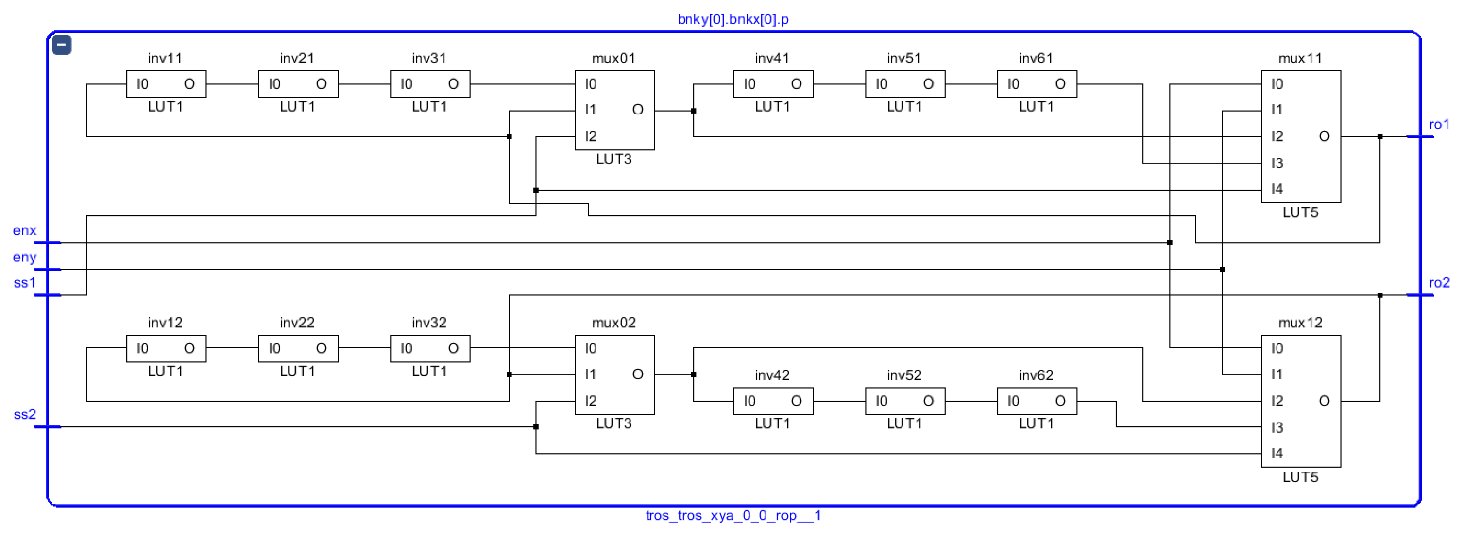
The design and characterization of a configurable RO-PUF for programmable devices that incorporate different strategies to minimize resource occupation and accelerate time response are described in this paper. To exploit the configuration options, facilitate its characterization, and simplify the integration on an embedded system, the RO-PUF is implemented as a parameterized IP-module with a standard connection interface for embedded processors. The behavior of the PUF in Xilinx Zynq-7000 devices is analyzed using 15 Pynq-Z2 boards, in which an embedded system containing 10 PUF instances in different locations of the device is implemented. The tasks of selecting PUF configuration parameters, applying successive challenges following different strategies for the comparison of RO pairs, and capturing the corresponding responses for their subsequent statistical treatment are carried out with a series of test programs developed, compiled and run using the embedded operating system available on the development board.
The paper is organized as follows:
Section 2 introduces an overview of RO-PUFs, including a review of the strategies followed in the proposals in recent years to select the output bits of the PUFs. The design of the proposed configurable RO-PUF is detailed in
Section 3: the PUF structure and its main characteristics are illustrated in sub
Section 3.1. The realization of the RO-PUF as an IP-module is explained in
Section 3.2. The implementation of a test prototype, including several PUFs in the same System-on-Chip (SoC) is depicted in
Section 3.3.
Section 4 presents the results of the battery of tests carried out to achieve a complete characterization of the configurable RO-PUF. Finally, the conclusions of this work are expounded in
Section 5.
2. An Overview of RO-PUFs
An RO-PUF consists of an array of ring oscillators made up of an odd number of inverters, forming a combinational loop. The frequency of oscillation of the RO is roughly calculated by the following:
where
is the number of stages of the
RO and
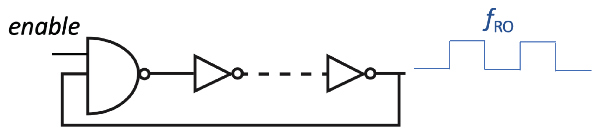
is the nominal time delay per inverter. The total delay in an RO loop must also consider the delays due to the paths connecting the active devices. According to this, two ROs with the same number of stages and an identical layout should have the same characteristic frequency. However, the variability inherent in the manufacturing processes of CMOS integrated circuits makes it such that each RO has a unique operating frequency, thereby providing a mechanism that allows the individual identification of different samples of the circuit. Usually, one inverter in the chain is replaced by a NAND gate to enable or disable the oscillation, as illustrated in
Figure 1.
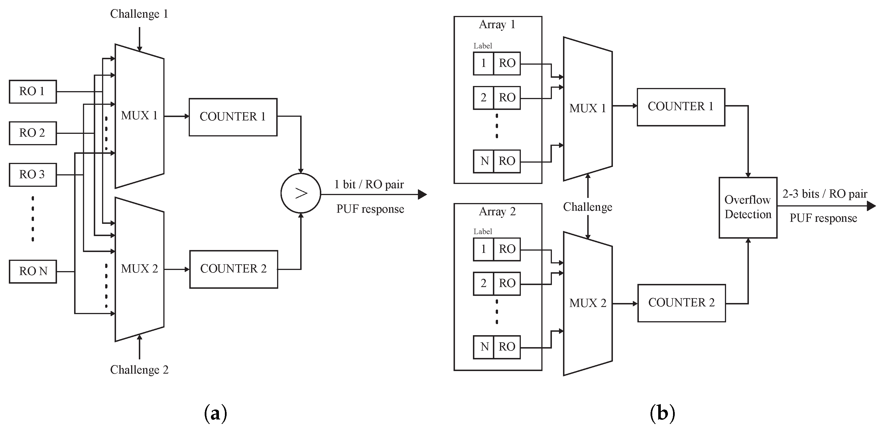
The conventional implementation of an RO-PUF, proposed in [
11], uses N identical ring oscillators whose outputs are connected to two multiplexers following the scheme in
Figure 2a. The selection signals of both multiplexers (
Challenge1 and
Challenge2) determine the RO pair to be compared, using their outputs as clock signals of two counters that compute the number of oscillations of each of the selected ROs in a time interval defined by a reference clock. The outputs of the two counters are then compared to produce a single output bit, whose value is 0 or 1 depending on which of the two ROs is faster. For a given pairwise comparison, the larger the frequency difference, the more reliable the corresponding response bit. Since this PUF provides one bit per each RO pair comparison, the generation of certain length bitstreams will require the implementation of a large number of ROs.
Certain physical phenomena (such as jitter, transistor-level noise sources, etc.) limit the repeatability of the PUF response, making it not directly usable in a secret key generation scheme as a consequence of not being perfectly reproducible, i.e., there are slight differences from run to run when applying the same challenges. The reliability of the PUF can also be affected by changes in its operating conditions (temperature, supply voltage, etc.). However, some techniques to implement PUFs highly robust to environmental variations were recently proposed in [
15], which implies a significant decrease in the relative importance of this type of effects. An additional problem is the lack of entropy due to the non-uniform distribution of the PUF response bits. Entropy is generally not at its maximum due to correlations between RO pair comparisons and bias in PUF output bits, i.e., the probability that a PUF bit has a specific value (‘1’ or ‘0’) is not
. The main causes of the lack of entropy are asymmetries in the PUF layout and systematic manufacturing variations [
16].
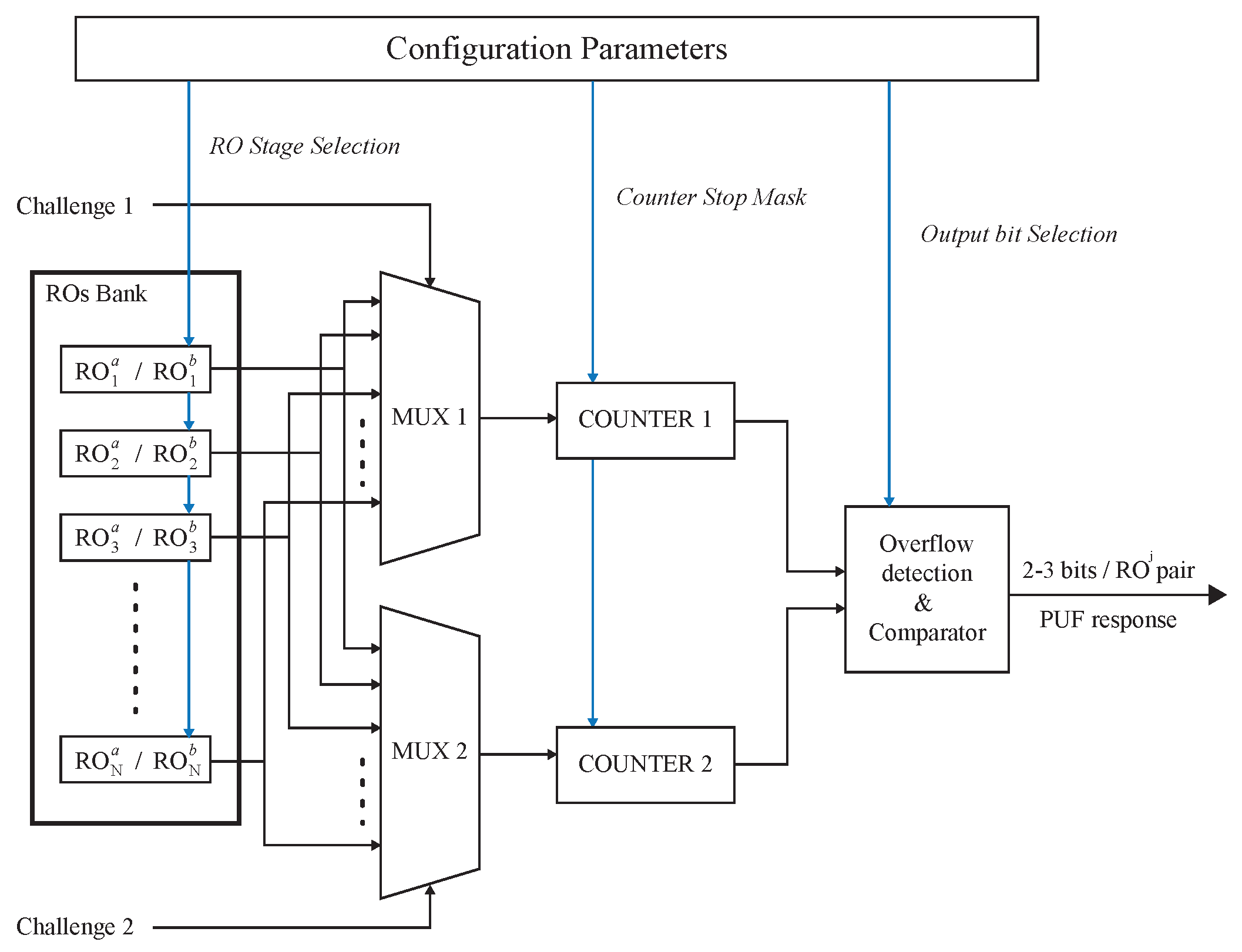
Figure 2.
Block diagrams of (
a) conventional RO-PUF in [
11], and (
b) RO-PUF presented in [
17].
Figure 2.
Block diagrams of (
a) conventional RO-PUF in [
11], and (
b) RO-PUF presented in [
17].
To fix these issues, the use of Helper Data Algorithms (HDA) is required to meet the key requirements [
16]. HDA encompass three concatenated building blocks: (1) bit selection to increase the reliability of the PUF response; (2) Error Correction Codes (ECC) to mitigate the effects of noisy PUF outputs [
18]; and (3) entropy increase to ensure that the distribution of 1 s and 0 s in the key is nearly uniform, usually performed by means of compression for the PUF output, using a hash function as first reported in [
19]. Several approaches have been proposed in the literature with the aim of improving the uniqueness and reliability of the bit sequence provided by an RO-PUF. As an example, transform-coding approaches based on different linear transformations were used in [
13,
15] to decorrelate data extracted from the ROs before being used in both the enrollment and the reconstruction stages of a fuzzy commitment scheme [
20]. Much effort has also been devoted to the study of ECCs (sometimes a combination of them) that can be efficient from the perspectives of security and resource consumption, the latter especially for resource-limited embedded system applications, such as IoT. Among the techniques that significantly reduce the size of the helper data, those that deserve mention include the use of ECCs based on polar coding described in [
21] or nested polar and Wyner-Ziv coding analyzed in [
22]. Other proposals use additional circuits to self-calibrate for better uniqueness and randomness. Among them, Ref. [
23] proposed a block that calibrates the phase to measure the RO frequency quickly and accurately. In addition to the pre- and post-processing techniques used to improve the quality of a secret key generation scheme, the complexity of the required ECCs can be reduced with a good selection of the bits that make up the PUF. Thus, many efforts have been focused in the selection of PUF output bits. PUF characterization is crucial to evaluate the reproducibility and entropy of its output, to the point that after PUF performance analysis, a partial or complete PUF redesign might be necessary to meet the PUF requirements.
In the context of RO-PUFs, bit selection is directly related to the selection of the two ROs that compose a pair. Several techniques have been presented in the literature to select the most suitable pairs of ROs and optimize the relationship between the PUF size (number of response bits) and the resources required to implement it.
Some commonly used methods to minimize the effect of correlated variations on RO-based PUFs include placing ROs as close as possible in a 2D array and selecting adjacent RO pairs in each comparison [
24]. Configuring ROs to select pairs with the largest differences of frequencies to increase the robustness of the PUF against environmental variations and noise is the approach followed in [
11], where only one of every eight possible RO pairs is used to conform the PUF, and in [
14,
24], where a Configurable Ring Oscillator (CRO) PUF that allows choosing the most suitable stages in each RO is described. Other proposals to improve the reliability of PUFs are based on generating enable signals to activate only the ROs to be compared at any given time [
25], choosing the most appropriate challenge–response set, as happens in the so-called ordering-based RO-PUFs [
26,
27], or selecting pairs of ROs based on their performance in a temperature range assuming that a temperature sensor is integrated on-chip [
28].
The size of a PUF must be large enough to provide secure keys of adequate length. Regarding the first requirement, to avoid possible correlations in the output bits of a PUF with N ROs, N/2 comparisons are frequently used in many of the proposed works [
11,
17,
29]. However, other authors take into account that there is no correlation if
pairs of neighboring ROs are used so that each RO participates only in two comparisons. Taking advantage of this circumstance, a comparison strategy is proposed in [
25] that also ensures that the compared pairs are implemented in physically adjacent locations within the FPGA fabric. On the other hand, the area-efficiency can be improved, resorting to the use of dynamic reconfiguration techniques provided by modern families of programmable devices [
30].
A strategy that simultaneously allows increasing the area-efficiency and reducing the response time of the PUF was proposed in [
17,
29]. Instead of using as the PUF output the bit resulting from the comparison of the counters (referred to as the “sign bit” in this work), this approach takes two or more bits from each RO pair whose values depend on the difference between the two counters, i.e., the difference in the oscillation frequency of the two ROs. The proposal, illustrated in
Figure 2b, uses two arrays with the same number of identical ROs. A unique challenge controls both multiplexers selecting ROs with the same labels in each RO bank. The oscillations of the selected ROs are simultaneously computed by the two counters. Unlike the conventional proposal in which the counting interval is fixed by an external source, in this case, the overflow of one of the counters marks the end of the evaluation period. Thus, the measurement is stopped as soon as one of the counters reaches its maximum value and the value of the other counter is used for further processing. The analysis of the PUF performance in a particular device determines which bits of the counter are used to generate the PUF output. Usually two or three bits are selected per comparison instead of the unique bit obtained with the conventional RO-PUF. The total bit number that is required to the PUF response depends on the application. For the sake of illustration, a key generation of 256-bits will require 128 runs if two bits are extracted from one measurement. Thus, the proposal in [
17] will halve the total resources and time to retrieve a key versus the conventional approach that only provides one bit per pair comparison.
4. RO-PUF Characterization
Pynq-Z2 is a low-cost development board compatible with the Python Productivity for the Zynq (PYNQ) environment [
32]. It provides a Python framework on an embedded Linux operating system, which simplifies the interaction between the hardware and software components of an embedded system. Hardware elements are integrated into PYNQ through “overlays” (the hardware equivalency to software libraries) to which a Python interface is associated to facilitate their use. In order to accelerate the system operation, however, in this work, we use, as an alternative to coding in Python, the C-API provided in [
33], which provides a similar functionality through a set of C routines that can be compiled to generate executable code.
Using these facilities, a complete test protocol is defined, coded as a set of C programs, and run on 15 Pynq-Z2 boards—all with the objective of characterizing experimentally the designed PUF and identifying those of the possible configuration options that should be selected to optimize the PUF behavior, both in terms of reliability and efficiency. The use of 15 boards and 10 PUFs implemented per board makes it possible to have a total of 150 samples to characterize the proposed RO-PUF, which ensures the generality of the results obtained.
Among the characteristics that are analyzed, it is worth highlighting the use of different strategies to select the pairs of ROs that are compared (which we refer to as the “test strategy” in this paper), the behavior of ROs with different configurations, and the influence of other configurable parameters (e.g., the number of counters’ bits, the size of the PUF, or the generation of enable signals to limit the number of ROs oscillating simultaneously).
The practical use of an RO-PUF requires establishing a challenge-response mechanism, which implies fixing a method to explore the elements of the RO bank and selecting the ROs that are compared. Among all the possible alternatives to select the two components of the pair to compare, we have chosen four different ways of matching the ROs based on their proximity and the type of Slice in which they are implemented. The characteristics of each of these “test strategies” are the following:
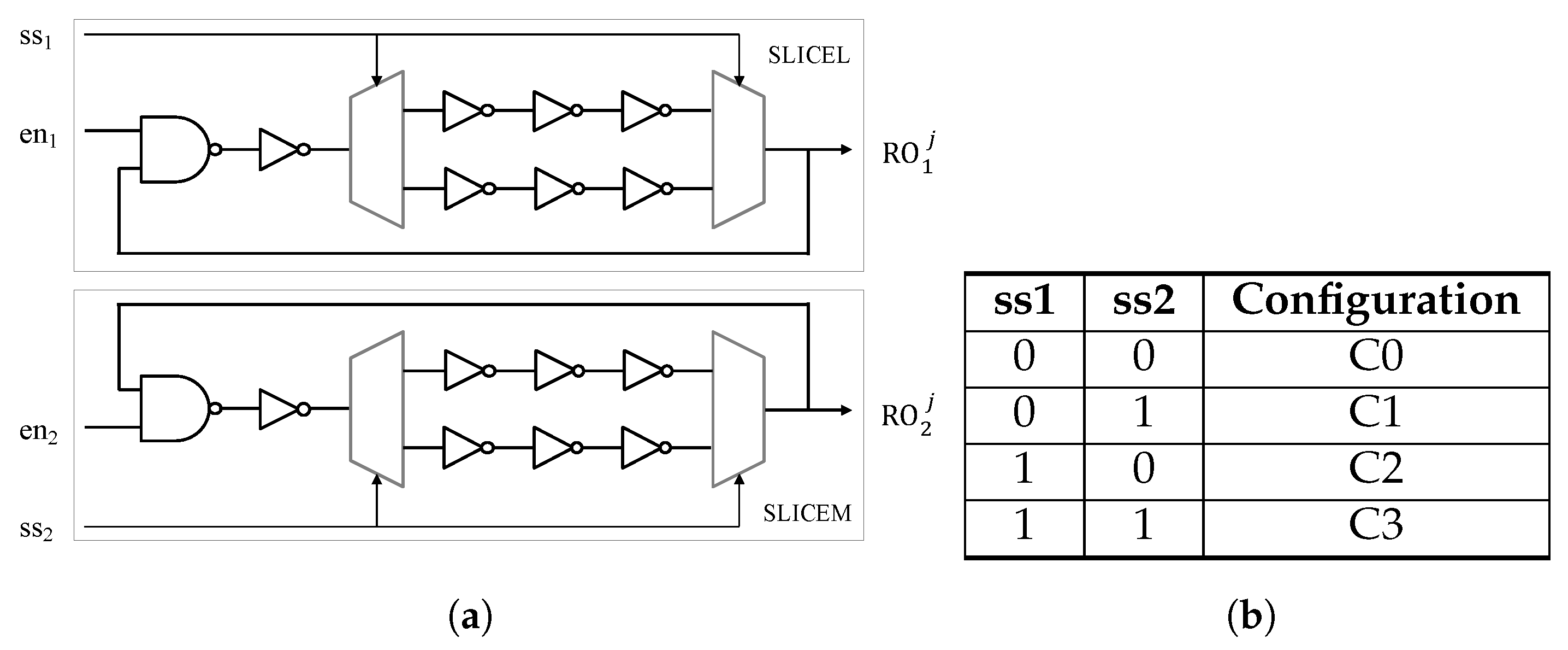
T01: The first test strategy consists of pairing the closest ROs with identical layouts. To perform this, the RO bank is traversed by rows to compare the RO implemented in a Slice with the one located in the Slice that occupies the same position in the next CLB (thus ensuring that both ROs correspond to Slices of type M or L). To avoid edge effects, the ROs in the last CLB of each row are not used as the first RO of a pair, so the maximum number of comparisons obtained with this test strategy is pairs for the test prototypes.
T02: This test strategy pairs the furthest ROs within the same layout. To do this, an offset equal to the number of CLBs (i.e., half the number of Slices) occupied by the RO bank is added to the selection input of the second multiplexer. The number of comparisons is in this case pairs.
T03: Two ROs in consecutive Slices are paired when using this strategy, which implies that one of them is implemented in a M-type Slice and the other one in a L-type Slice. Now, only the RO in the last Slice of the last CLB in each row is not used as the first RO of a pair to avoid edge effects, being the number of possible comparisons pairs.
T04: The last test strategy compares the furthest ROs implemented in Slices of different types by adding an offset equal to the number of CLBs plus one to the selection input of the second multiplexer. The number of comparisons is pairs.
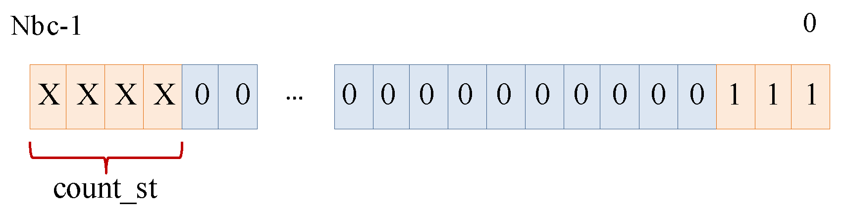
In order to characterize the suitability of the different IP-module outputs to generate the PUF response, a set of tests based on the four previously described strategies is first run for the 15 available boards. In each test, the same sequence of challenges is applied 1000 times and the two IP-module outputs (sign bit and counter value corresponding to the slowest RO) are captured and stored in output files. The use of stage_selection bits to analyze all possible RO configurations in each CLB, a stop_c mask to limit the effective size of the counters to 15 bits, and the option to generate row and column enable signals for CLBs are the alternatives configured to perform this test battery.
To reduce the processing time when analyzing the data, only one in five of the comparisons made in each test are considered in the calculations (280 for T01, 300 for T03, and 320 in the case of T02 and T04). In this way, it is ensured that a similar number of ROs of the four possible configurations (C0-C3) participate in the PUF output.
In addition to the sign bit, which is the only alternative for PUFs whose response depends on which is the fastest of the two ROs involved in each comparison, in those that measure the value of the frequency difference between the two ROs, one or more bits of the value resulting in each comparison can be used as PUF response according to the measures of stability, probability and entropy that they provide [
17].
The stability (
s) of a bit at position
i for a particular RO is defined as follows:
where
is the probability of occurrence of 1 at position
i as follows:
being that
k is the number of responses obtained (
for each test) and
the
i-th bit of the
j-th response value. The average stability (
S) is calculated, taking into account the total number of RO pair comparisons in each test, noted as
N:
To corroborate if the PUF output fulfills the uniqueness requirement, two metrics of entropy are evaluated: the intra-entropy (Hintra) to evaluate the uniqueness of the PUF output bits within each PUF implementation, and the inter-entropy (Hinter) to evaluate the bit uniqueness for each of the RO pairs in different PUF implementations. The average intra-entropy of bit position
i is defined as follows:
where
m is the number of implementations, calculated as the product of the number of devices (
) and the number of different RO-PUFs implemented on each device (
), i.e.,
, and
is the probability of message
q within the
j-th implementation with only two possible messages:
where
represents the
l-th RO pair on the
j-th implementation,
n is the number of RO pairs, and
is the majority value of the
i-th position determined from
k responses evaluated for each pair of ROs.
The average inter-entropy of bit position
i is computed as follows:
where
is the probability of message
q of
l-th RO pair:
The ideal value for the stability is 1, which means the bit output is reproducible in all the responses. However, this condition can be relaxed, and a value higher than 0.95 is considered acceptable. Concerning probability, its ideal value should be equal to 0.5 to avoid bias but small variations (±0.015) are accepted. A maximum entropy (Hintra and Hinter) equal to 1 guarantees that there is no correlation between the different output bits at each PUF and there is no correlation between bits on the same positions among different implementations. Again, small fluctuations of entropy are tolerable if the average values of intra- and inter-entropy surpass 0.95. Compression can correct the impact of correlations and bias of the PUF to increase entropy [
16]. As result, the key derived from PUF will be nearly uniform.
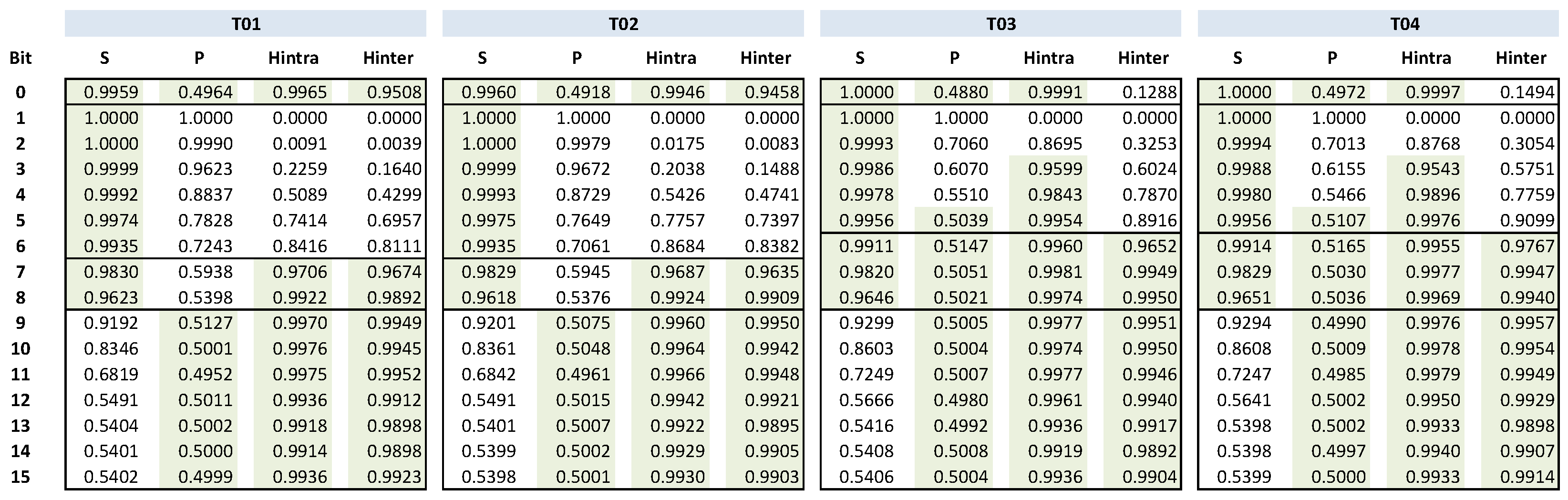
Figure 9 shows the average values of stability, probability, Hintra and Hinter among different RO pairs for the sign (bit 0) and bits 1–15 of the counter value (To facilitate comparison when using counters of different sizes, bit 1 corresponds to the MSB and bit 15 to the LSB.) obtained as outputs of the 10 implemented PUFs when the tests are run for the 15 Pynq-Z2 boards. The results highlighted with green background satisfy the tolerable values in the average stability, probability and entropy, i.e., values between 0.95 and 1 in the case of Hintra, Hinter, and stability, and values between 0.485 and 0.515 in the case of probability.
Figure 9 shows two clearly different behaviors. When using test strategies T01 and T02, the sign bit is a good candidate to be included as a PUF response since it presents a stability very close to the ideal value of 1, Hintra and Hinter values that are sufficiently large, and a probability also close to the ideal value (0.5 in this case). However, none of the counter bits simultaneously satisfy the four required conditions, although bits 7 and 8 do satisfy three of them, failing at the probability requirement. On the contrary, data corresponding to test strategies T03 and T04 show that the sign bit should not be chosen in this case since the value of Hinter is extremely low. Nevertheless, there are three bits of the counter value that fulfill all necessary requirements and, thus, should be considered and subsequently analyzed to form part of the PUF response.
The choice of the bit or set of bits that forms the PUF response when each pair of ROs is compared is determined by the uniqueness and reliability of the device. These properties can be quantified by evaluating the Hamming distances between the codes resulting from the repeated application of the challenges sequence to the same PUF (HDintra) and to other replicas of it deployed in other locations on the same development board or in the same location on different boards (HDinter), respectively.
The intra-Hamming distance is estimated as follows:
where
m and
k have already been defined, and
is the reference response calculated as the mode over all responses.
The uniqueness is calculated via the inter-Hamming distance, defined as follows:
As for HDinter, 50% is the optimal value for this metric, although we accept as tolerable values with an error of . The desirable value of HDintra is 0, which means that the response that produces a given PUF implementation is always the same. However, if these values are not so low, the response of the PUF could be improved with the use of ECCs, as explained in the introduction.
With the idea of reducing the time taken to complete the analysis, before proceeding with an exhaustive processing of the captured data, a series of specific tests are carried out to determine the influence of the different PUF configuration parameters.
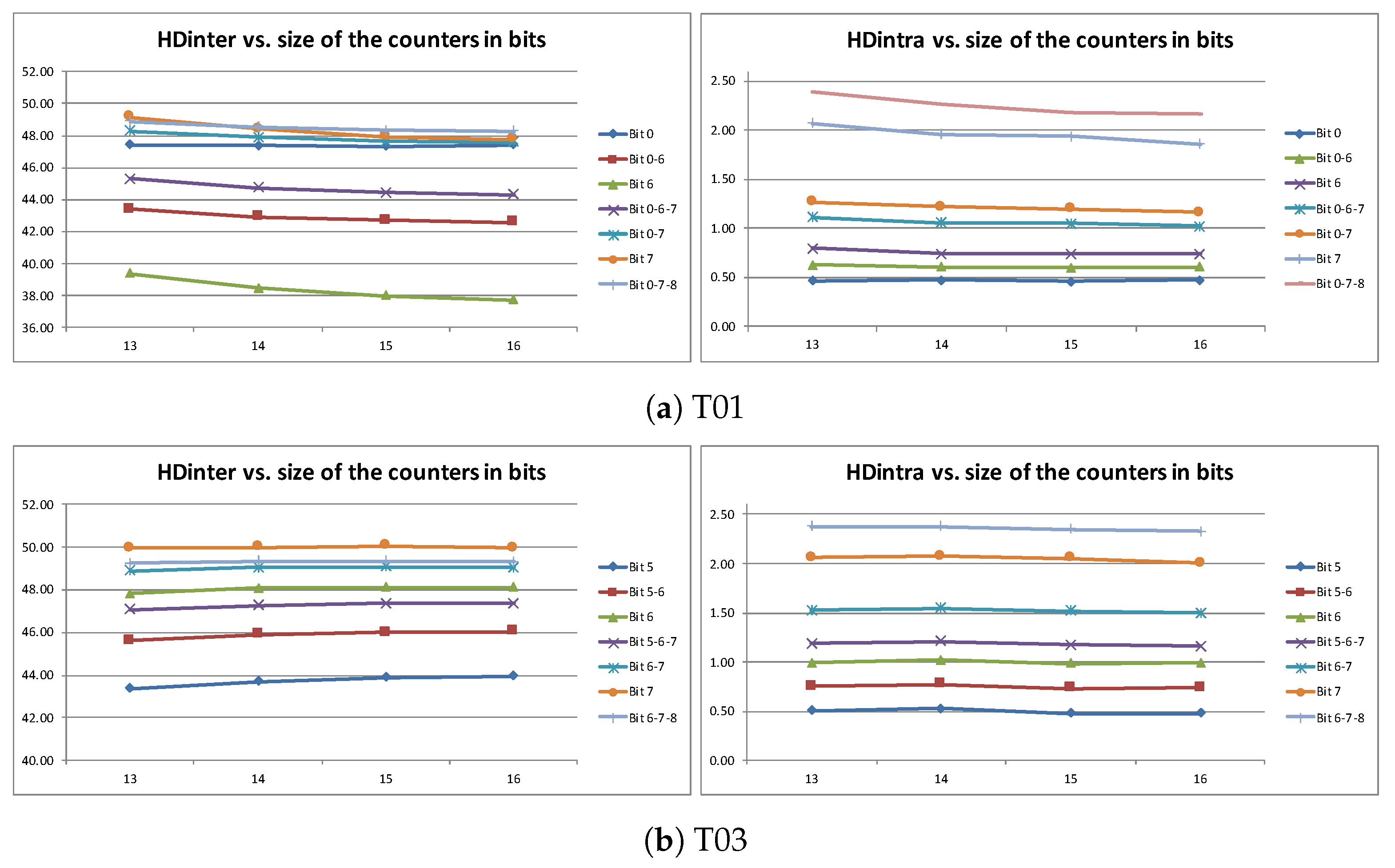
The first of these tests aims to characterize the influence of the size of the counters to determine the number of bits that allows to minimize the PUF response time without degrading its quality indexes. Data are obtained by executing the four test strategies varying the sizes of the counters from 13 to 16 bits, using for this purpose the stop_c mask configurable through the control input register of the IP-module.
Figure 10 illustrates the total HDinter and mean HDintra values obtained after processing different combinations of the outputs bits of the comparisons for 1000 responses of 50 PUFs implemented in five different programmable devices. To save space, only results corresponding to test strategies T01 and T03 are included in
Figure 10. Those related to the other two strategies show a very similar behavior. From the results, it can be seen that both HDintra and HDinter remain almost constant for
values above 13 bits. In the rest of the analysis,
is selected, as it is the smallest size that offers a good trade-off between HDintra and HDinter for all test strategies.
Two other parameters are analyzed to guarantee the generalization of the conclusions obtained in our study: the number of samples (PUF implementations at different locations inside a programmable device and/or on different boards) that should be used, and the size of the PUF (i.e., the number of pairs of ROs compared when applying the challenge sequence) from which the extracted statistic faithfully represents the behavior of this type of RO-PUF. As far as the number of samples is reduced, the evaluation time decreases.
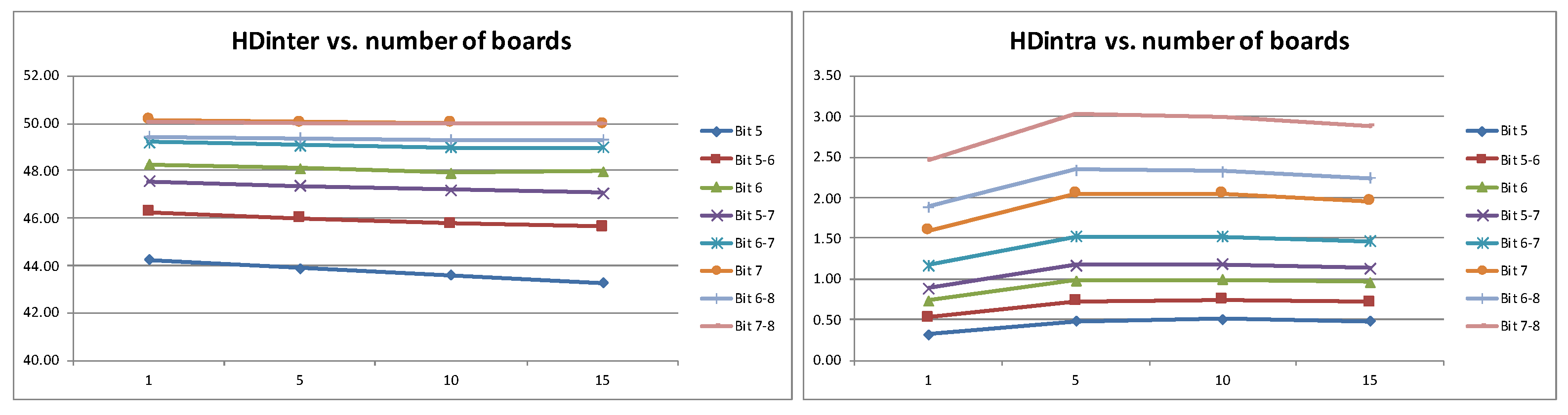
To perform this study, data collected from the 15 development boards are used, first processing the data from a single board, then from 5, later from 10, and finally from all the available boards. The impact of the number of samples on the measures that characterize the quality of the PUF is illustrated in the graphs of
Figure 11 (once again, only results corresponding to the run of T03 are shown, although the trend is similar for the other considered test strategies). Analyzing the graphs, the values of HDinter and HDintra obtained with a single board (10 RO-PUFs) are worse than in the rest of the cases, but the differences are much smaller when 5 boards (or more) are used, especially for the combinations of bits that enhance each of these figures of merit (bits 6 and 7 for HDinter and bits 5 and 6 for HDintra). Therefore, the statistical results corroborate that processing 5 boards, that is, 50 RO-PUFs, is adequate to represent a generic implementation of the PUF.
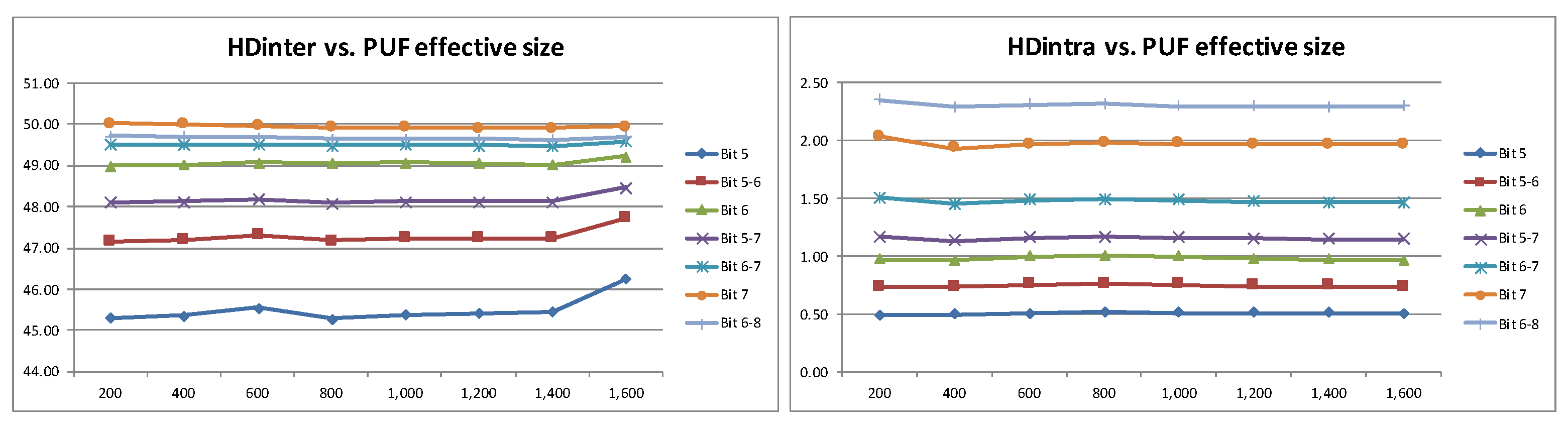
Finally, it is convenient to evaluate whether the results obtained from a partial sampling of the RO pairs available in the PUF can be extrapolated when the sample size is progressively increased until all possible pairs.
Figure 12 shows the evolution of HDinter and HDintra values for different bit combinations as a function of the number of RO pairs that contribute to the PUF response, i.e., the effective size of the PUF. Test strategy T04 is the option selected for this study. As can be seen, the two quality indexes are almost independent of the PUF size, but for the smaller sampled data, the worst results are obtained. However, from 400 RO pairs onward, the values obtained can be acceptably extrapolated to any PUF size.
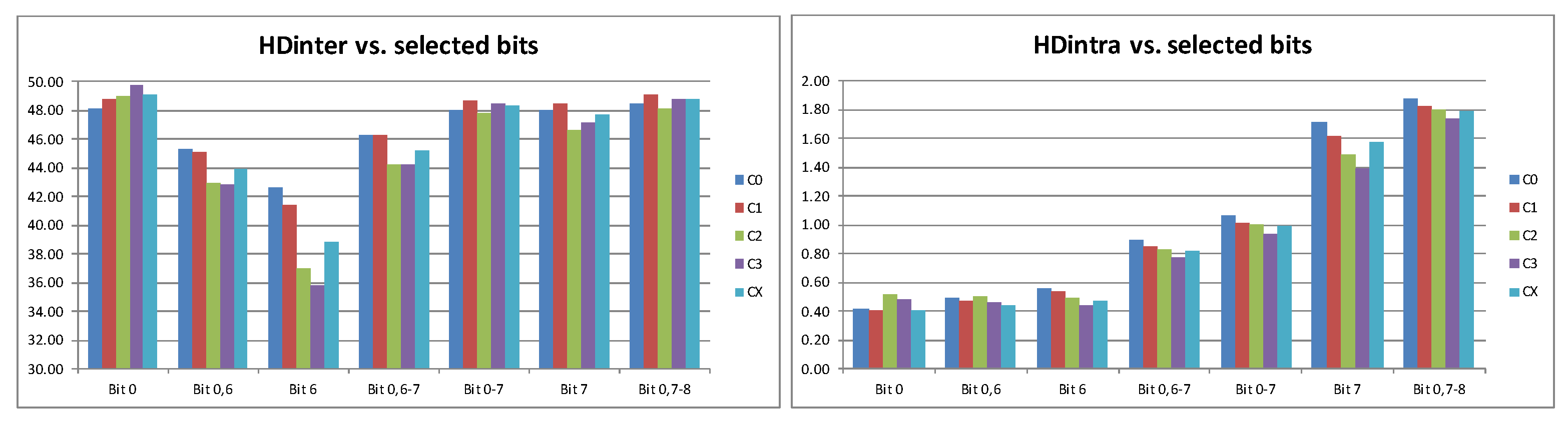
Once the necessary conditions to obtain generalizable results through specific tests are determined, the calculation of HDinter and HDintra values associated with the different test strategies and the possible RO configurations can be completed. This analysis is carried out using 200,000 PUF responses, collected from 5 Pynq-Z2 boards when executing the four test strategies, with 15-bit counters, and the option to generate enable signals. The data of each PUF are grouped in five blocks of 400 samples, four corresponding to the possible configurations of the ROs in a CLB (C0–C3), plus a fifth one (CX) that homogeneously combines elements of the 4 configurations. Test strategy T02 is the option selected in this occasion to carry out the study.
Figure 13 shows that the influence of the type of ROs that is selected is not decisive. The values of HDintra are worse when selecting bits 6 and 7 in the C2 configuration; however, if we take PUF responses that combine pairs of ROs with different combinations, the results of HDintra are good enough, with acceptable low values of HDinter. So we can conclude that the results that combine different pairs follow the representative trend among all, so we do not need to discard any of the configurations a priori. Therefore, the number of possible answers for the same PUF design can be increased.
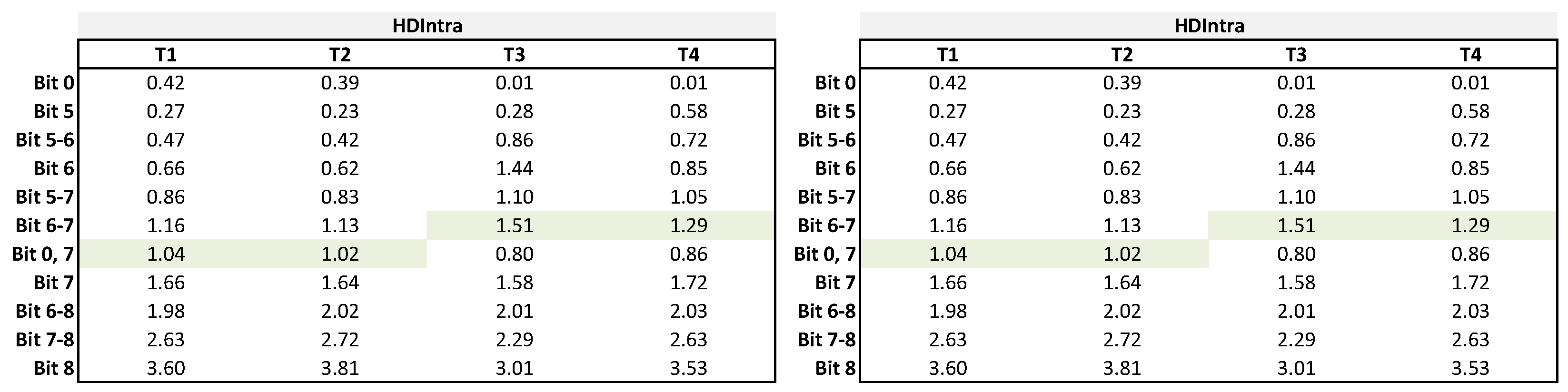
After analyzing the previous results, the settings for a final exhaustive study of HDintra and HDinter include 15-bit counters, 5 boards, 400 samples, enabling only the selected ROs, and a CX configuration. We evaluate all the strategies tested for all the interesting bits for each test in order to determine which of them provides better results in terms of HDinter and HDintra as shown in
Figure 14. The candidate bits for T01 and T02 are the sign bit (bit 0) and bits from 5 to 8, as indicated the preliminary results in
Figure 9. In the case of tests T03 and T04, bits from 6 to 8 offer the best performance. Finally, we also calculated the HDintra and HDinter among different RO-PUFs compounded by a combination of these bits in all the possible tests.
Figure 14 shows the RO-PUFs that offer the best trade-offs between HDintra and HDinter (cells with background in green), that is, the lowest values of HDintra with a tolerable value of HDintra (
). The PUF generated by selecting bit 0 and 7 offers the best performance using tests T01 and T02, while the PUF generated by selecting bit 6 and 7 offers the best performance using tests T03 and T04.
5. Conclusions
Properly combining some of the techniques previously reported in the literature, and taking full advantage of the resources available in the CLBs of Xilinx 7-Series programmable devices, this paper describes the design and characterization of a configurable RO-PUF efficient both in terms of occupied resources and operation speed.
The core of the PUF is an array of CLBs. Each CLB implements two configurable 5-stage ROs, in which two possible options that share two logical elements of the eight available at each CLB Slice can be dynamically selected. In this way, it is possible to consider four different alternatives when comparing a pair of ROs located in different CLBs, which allows multiplying by four the effective size of the PUF.
The length of the PUF response can also be increased if more than one bit is selected from each RO pair comparison. Two non-exclusive approaches are included in the design for this purpose. One of them consists of using the “sign bit” given by the overflow signal of one of the counters used to compare the oscillation frequencies of the two ROs. The second one is based on selecting one or more bits of the counter that does not overflow after the comparison.
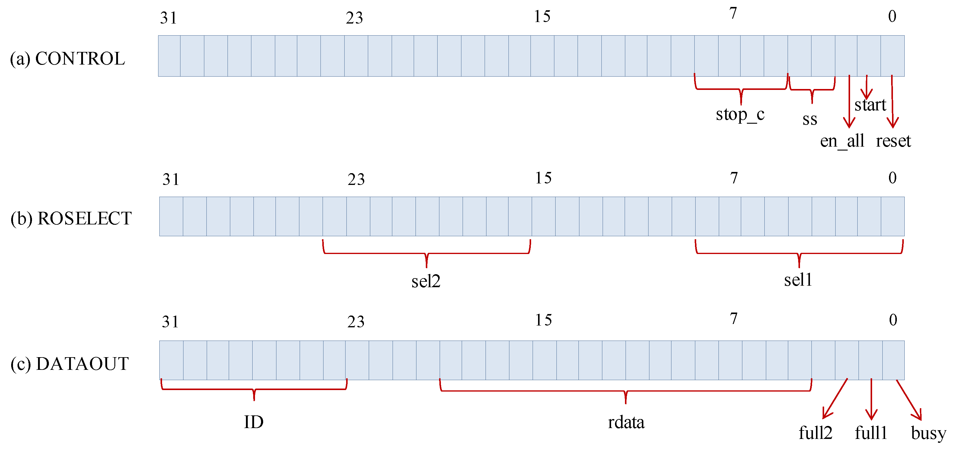
The proposed RO-PUF is conceived as a parametrizable IP-module that incorporates a standard AXI4-Lite interface to facilitate its integration into embedded systems. The size of the RO bank and its location on the programmable device can be chosen prior to the synthesis and implementation process. Other aspects of the PUF functionality (such as the size of the counters, the generation of enable signals, or the strategy of applying the challenge sequence) can be dynamically chosen during the characterization and operation phases, using the I/O registers mapped into the memory space of the embedded processor.
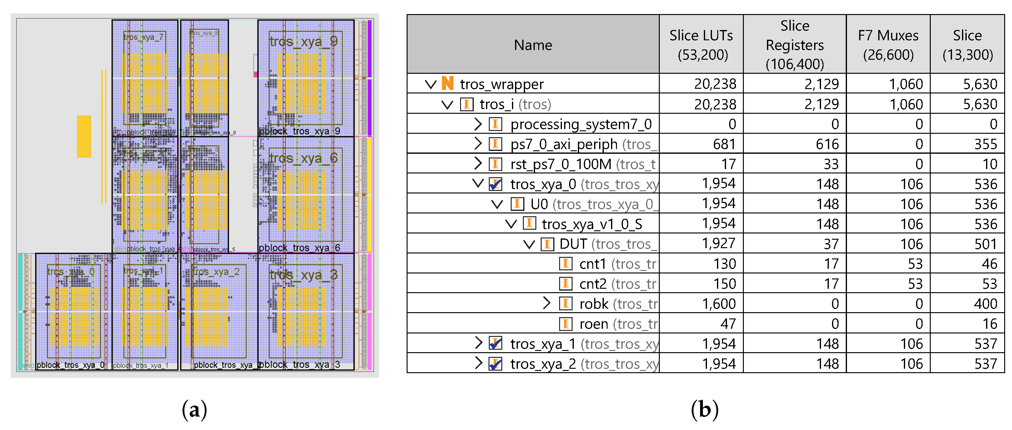
Using these facilities, an exhaustive battery of tests was carried out in order to analyze the influence on the PUF quality indexes of different parameters and options. The tests were executed on 15 Pynq-Z2 development boards implementing a design that incorporates 10 PUFs with a -CLB RO bank (400 configurable ROs). The results included in the paper illustrate the procedure for the bit selection of the PUF response (sign bit and/or counter bits) that allows establishing adequate trade-offs between reliability and uniqueness metrics.
Among the future lines of continuity of this work, it is worth mentioning the realization of a deep statistical study with the idea of having a theoretical basis for the selection of bits that corroborates the experimental results obtained in this paper, as well as the use of PUF responses in the development of a secret key generation and recovery scheme efficient in terms of security and resource consumption.


