Article

Linearization Technique of Low Power Opamps in CMOS FD-SOI Technologies

Faculty of Electronics and Information Technology, Institute of Microelectronics and Optoelectronics, Warsaw University of Technology, 00-661 Warsaw, Poland
Electronics 2021, 10(15), 1800; https://doi.org/10.3390/electronics10151800
Submission received: 14 June 2021 / Revised: 16 July 2021 / Accepted: 23 July 2021 / Published: 27 July 2021
(This article belongs to the Special Issue Low-Voltage Integrated Circuits Design and Application, Volume II)

Abstract

:
Negative feedback applied to the back gate of MOS devices available in FD-SOI (fully depleted silicon on insulator) CMOS technologies can be used to improve the linearity of operational amplifiers. Two operational amplifiers designed and fabricated in a 22 nm FD-SOI technology illustrate this technique, as well as its advantages and limitations.

1. Introduction

In comparison with the mainstream bulk CMOS, CMOS FD-SOI technology [1,2] provides a set of benefits for analog circuits, such as better transconductance efficiency (gm/ID), higher bandwidth (fT and fmax), better matching, and lower subthreshold leakage. It has also been demonstrated that FD-SOI CMOS can be a technology of choice for cryogenic integrated circuits [3,4]. However, a really unique feature of FD-SOI MOS devices is that they are double-gate transistors. The semiconductor region under the transistor channel (called similarly as in the bulk CMOS: N-well or P-well) is isolated from the channel by a buried oxide (BOX) layer and can be used as the second, namely the back gate. N-wells are isolated from the p-type substrate by a pn junction. P-wells can also be isolated from the p-type substrate by the third deep well (Figure 1). This allows for applying a bias voltage to N-wells as well as to P-wells. Back bias, i.e., voltage applied to the back gate, can be applied to each device individually or to a group of devices located over a common P-well or N-well.
Back bias allows for changing the threshold voltage VT as seen by the front gate and fine tune the performance and power consumption of FD-SOI-based circuits.
It is worth noting that FD-SOI technologies can be technologies of choice for ultra-low voltage CMOS circuits. With proper back bias, the supply voltage in digital circuits can be reduced to 0.4–0.5 V. Such a reduction is more difficult in the case of analog circuits, but even without it, the maximal supply voltages in industrial deep submicron FD-SOI technologies are at the level of 0.8–1 V.
While in digital circuits back bias is applied as a constant (but often variable) voltage, in analog circuits, AC signals can be applied to the back gate as well (see, e.g., [5,6,7]). This creates new opportunities for analog circuit design. However, in the majority of analog circuits published so far, back biasing is used in a similar way as in digital circuits—to enhance or the tune circuit performance by means of DC forward or reverse back bias (see, e.g., four amplifiers [8,9,10,11]).
It has been shown experimentally in [7] that a negative feedback loop between the output and the back gate of one of the input transistors can very effectively linearize the characteristics of an operational amplifier. This paper extends the results published in [7] in the following ways: it provides a theoretical analysis of this linearization technique, including its limitations, in Section 2, and Section 3 also describes another amplifier, in which this linearization technique was used. In Section 3, the characteristics of these two opamps designed and fabricated in 22 nm FD-SOI technology are compared with theory. It is also shown how this linearization technique affects the frequency response and variability of the amplifiers. Conclusions and possible extensions of this linearization technique are presented in Section 4.

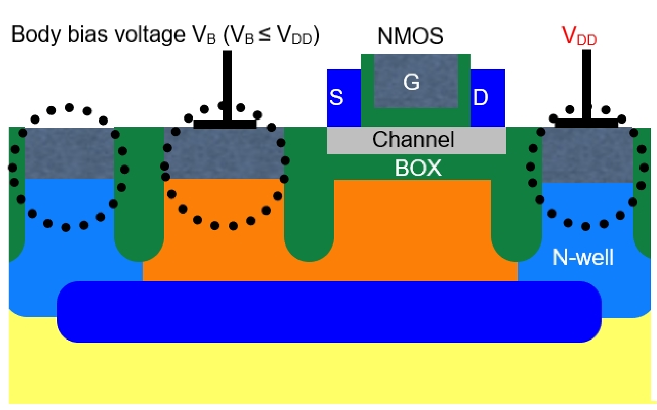
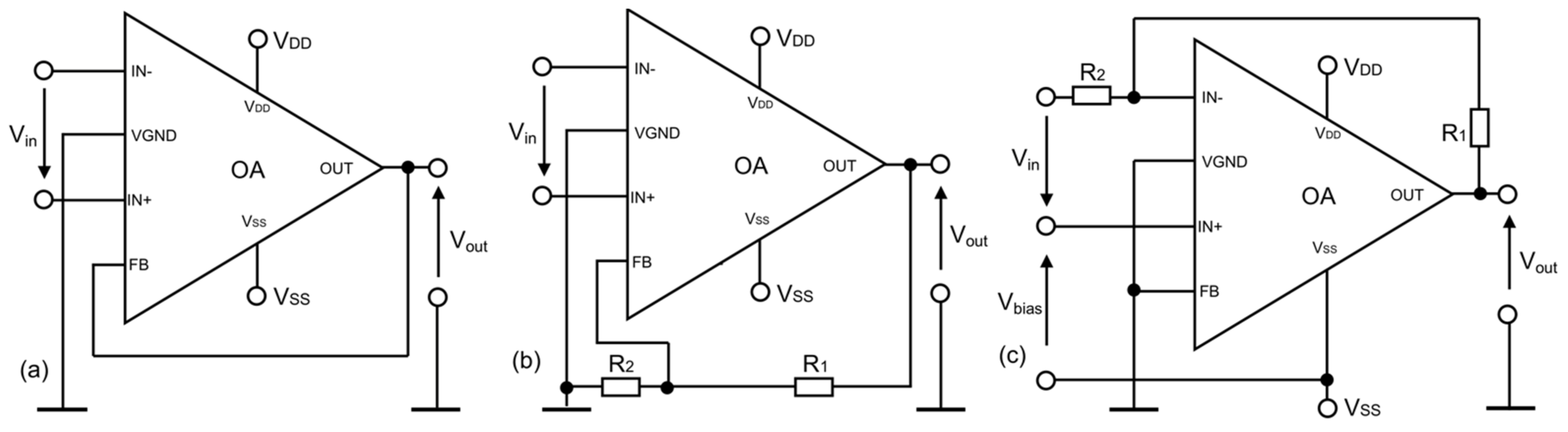
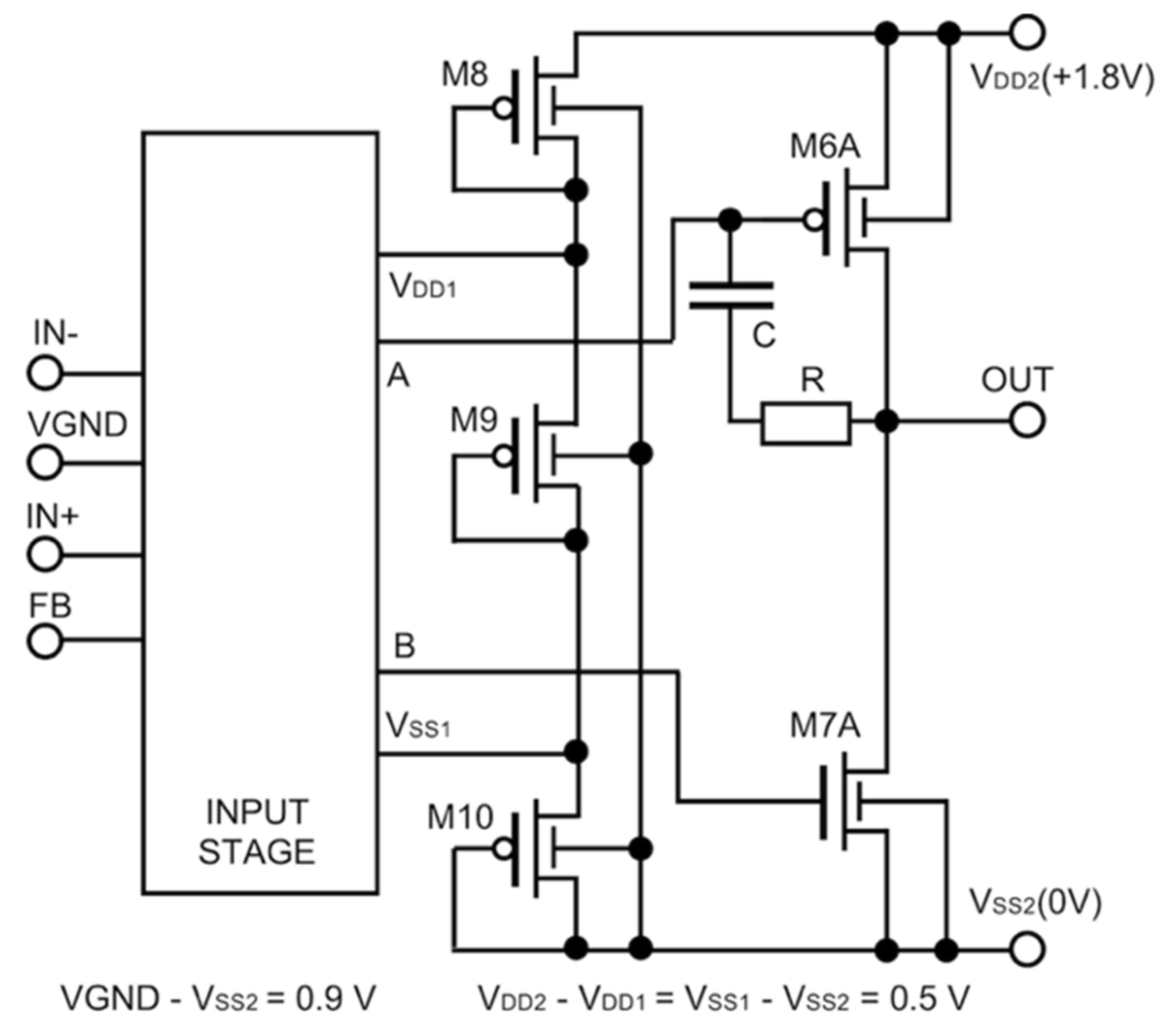
2. Opamp Linearization Technique: The Concept and Theory

Many methods of linearization of operational amplifiers’ characteristics, applicable to bulk CMOS technologies, have been proposed, see, e.g., [12,13,14,15,16,17,18,19]. In this paper, a technique is proposed that is specific to CMOS FD-SOI: a negative feedback loop between the output of the opamp and the back gate of one of the transistors in the input differential pair, see Figure 2.
The front gates of the devices of the input differential pair are driven by the input voltage vin and the back gates of these devices are driven by the output voltage vout. The output voltage of the input differential pair v1 is given by
v 1 = v i n g m f v o u t g m b g d s 2 + g d s 4
where gmf is the transconductance related to the front gate of M2; gmb is the transconductance related to the back gate of M2; and gds2 and gds4 are output conductances of M2 and M4, respectively. The output voltage of the input differential pair is amplified by the second stage with voltage gain ku2:
v o u t = k u 2 v i n g m f g d s 2 + g d s 4 k u 2 v o u t g m b g d s 2 + g d s 4
This gives the voltage gain ku of the amplifier with the feedback loop
k u = v o u t v i n = g m f g d s 2 + g d s 4 / k u 2 + g m b
It can be safely assumed that g d s 2 + g d s 4 / k u 2 g m b . As a result, the voltage gain ku can be approximated with good accuracy by
k u = v o u t v i n g m f g m b
This small signal analysis suggests the necessary linearity condition of the feedback loop. The ratio g m f / g m b must be constant in the whole range of gate voltages at the front and back gates VGSf and VGSb and the drain current ID of the input transistors. This condition is satisfied when the input transistors work in a weak inversion region for all combinations of the front and back gate voltages. In the weak inversion, the transconductance efficiency g m / I D is constant. It is demonstrated in [20] that both transconductance efficiencies g m f / I D and g m b / I D are constant in a weak inversion. As the drain current is, of course, the same for both gates, gmf and gmb are proportional to each other and their ratio is constant.
In Section 3, the properties of two simple OTA (operational transconductance amplifier)-type amplifiers, to be used for the acquisition of biological signals, are discussed. They have been designed and fabricated in an industrial 22 nm FD-SOI technology. Their properties will be discussed in three configurations (Figure 3).
In these schematic diagrams, VGND is the virtual ground. The voltage at this node equals 0.5 V D D . FB is the connection to the back gate of the transistor M1. In the first configuration (Figure 3a, direct feedback configuration) the output voltage is applied directly to the body of M1, as in Figure 2. In the second configuration (Figure 3b, feedback with voltage divider), the output voltage applied to the body of M1 is reduced by a voltage divider R1–R2. This is equivalent to a reduction of gmb in (4) by R 2 / R 1 + R 2 . If g d s 2 + g d s 4 / k u 2 g m b R 2 / R 1 + R 2 , the voltage gain is as follow:
k u = v o u t v i n g m f g m b R 1 + R 2 R 2
The voltage divider can be used to adjust the voltage gain to any value between the minimal gain (3) and the maximal gain that is obtained without direct feedback, i.e., when no output signal is applied to the back gate of the input transistor. The maximal gain is given by
k u m a x = k u 2 g m f g d s 2 + g d s 4
From (3) and (6), a general expression for the voltage gain, in terms of the minimal gain kumin and maximal gain kumax, is obtained
k u = k u m a x k u m a x g m b g m f   R 2 R 1 + R 2 + 1 = k u m a x k u m a x k u m i n   R 2 R 1 + R 2 + 1
where it is assumed that the minimal voltage gain is given by (4) with sufficient accuracy.
As it will be shown in the next section, the minimal gain of the amplifiers discussed in this paper is quite small. It is sufficient for the purpose for which these amplifiers were designed, but for other applications, a much higher gain may be needed. A higher gain can be obtained with the voltage divider R1–R2 (see (5) where R 1 + R 2 / R 2 is always larger than 1); however, a reduction of the feedback signal by the divider results in a reduced range of linearity of the response of the amplifier. When R1 is very large, ku reaches kumax and the linearization effect vanishes.
It is worth noting here that bulk-driven CMOS circuits, i.e., the circuits in which AC signals are applied to the bodies of the MOS devices, are well known [17,18,19,21,22,23,24,25,26]. However, in bulk CMOS technologies, the linearization technique described here would not be possible. The body (either N-well or P-well) of a MOS device in bulk CMOS technologies is separated from the channel by the depletion region, not by BOX dielectric, and by pn junctions from the source and drain regions. This limits the range of voltages that can be applied to the body because reverse bias of the body vs. the channel means that the source and drain must be maintained.

3. Experimental Results

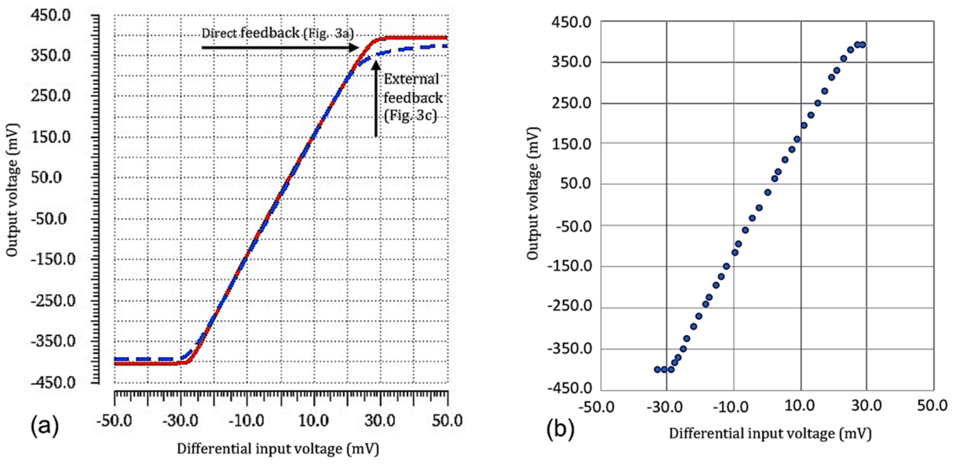
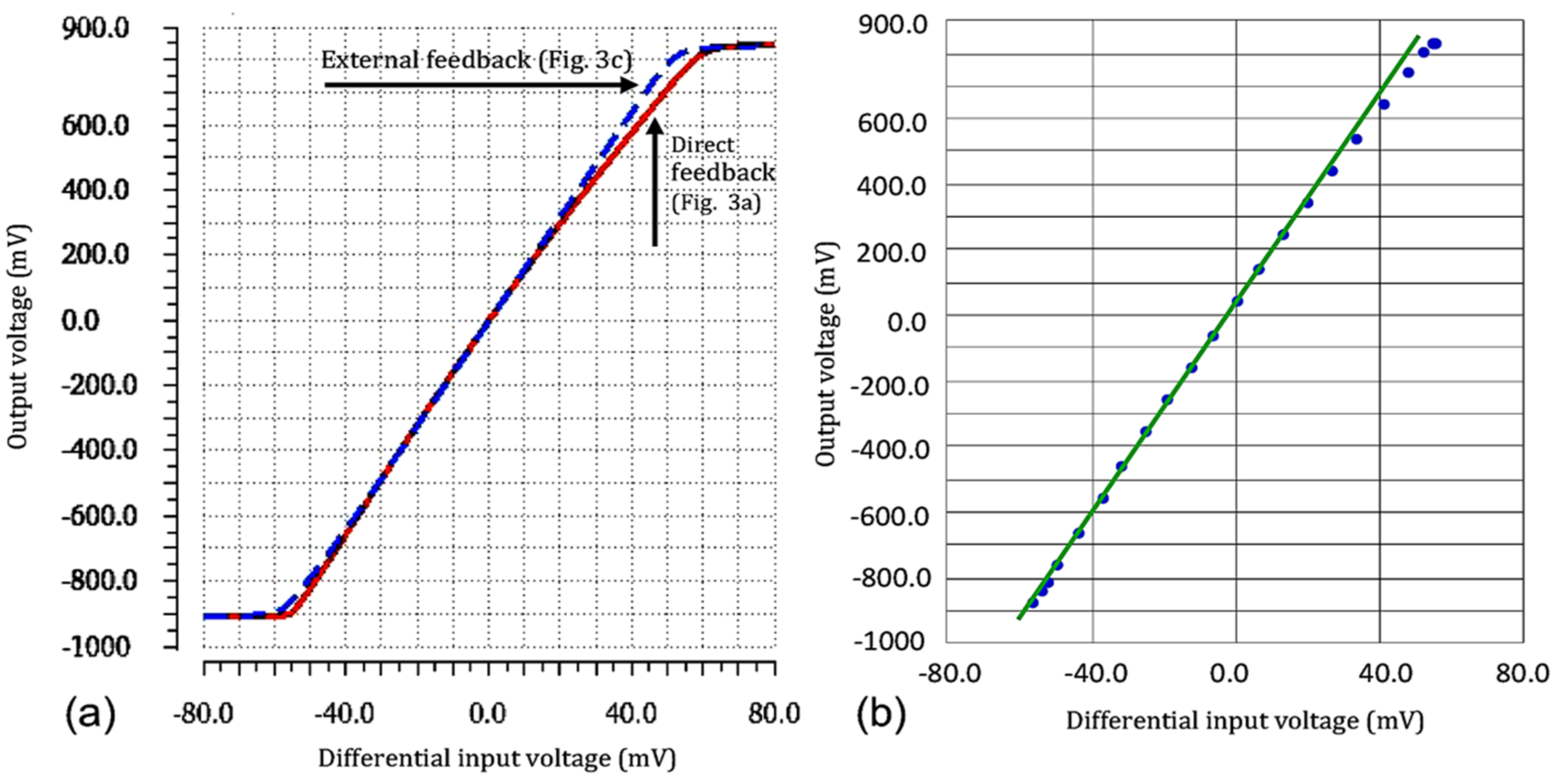
3.1. The First Amplifier

The first amplifier is shown in Figure 4. Its supply voltage is 0.8 V. Such a low supply voltage dictates the simplest OTA-type amplifier architecture, without more than three MOS devices in series between the supply and ground. A detailed description of this amplifier, including the layout and results of the measurements (voltage gain, input offset, bandwidth, noise, and power consumption) can be found in [7]. In [7], the performance of the first amplifier is also compared with other CMOS operational amplifiers, including one that is FD-SOI based [9].
The input transistors M1 and M2 are located over P-wells isolated from the p-type substrate by deep N-wells. Electrical contacts to the wells are located in “hybrid” regions where the BOX has been removed (Figure 1). Deep N-wells are connected to VDD1 (connection not shown in Figure 4). The voltages applied to the isolated P-wells, in particular output voltage applied to the P-well of M1, are always lower or equal to VDD. As a result, a reverse bias of all pn junctions is maintained.
Figure 5a shows the simulated response of the amplifier. Simulations were performed with device models provided by the foundry. The curve labeled “direct feedback” shows the response in the direct feedback configuration (Figure 3a). For comparison, the curve labeled “external feedback” shows the response obtained in configuration with external linear negative feedback (Figure 3c). The resistances R1 and R2 and the bias voltage Vbias were chosen in such a way that both curves match for the differential input voltage Vin equal to zero. The simulated response (Figure 5a) has been confirmed experimentally. Figure 5b shows measured response in one of 50 fabricated and measured prototype chips.
The direct feedback from the output to the body of the input transistor gives a linear response extending almost “rail to rail”.
Experimental results are in agreement with (4). Transconductances of M1 obtained from the simulation for the differential input voltage equal to zero are g m b = 0.523 × 10 6 A / V , g m f = 7.64 × 10 6 A / V . This gives k u = 14.616   V / V . The measured voltage gain (average for 49 fabricated chips [7]) is 14.5 V/V.

3.2. The Second Amplifier

Figure 6 shows the schematic diagram of the second amplifier.
The design goal of the second amplifier (Figure 6) was to increase the maximum output amplitude to 0.9 V. This amplifier is similar to the first one. The input stage is the same. In the output stage, transistors for 1.8 V maximum VDS and VGS were used. The supply voltage for the input stage is 0.8 V, as in the first amplifier. The voltage divider M8–M10 is the source of this voltage. Deep N-wells are connected to VDD2 (+1.8 V) (connection not shown in Figure 6). The layout of the second amplifier (Figure 7) is very similar to the layout of the first one shown in [7].
The input transistors M1–M2 (Figure 4) are visible at the upper left corner. Each transistor is divided into two connected in parallel in the common centroid configuration. Each of these four transistors is internally designed as four arrays of 100 relatively small (W/L = 10 μm/90 nm) devices. All of the other transistors are also designed as arrays of smaller devices. The big M5 (Figure 4) device can be seen as three rows of arrays of smaller transistors in the bottom part of the layout. The empty space between these rows is needed to meet the layout density rules. The big rectangle in the upper right corner is a MOM capacitor C. The divider (transistors M8–M10) and the output transistors M6A and M7A can be seen in the upper right part of the layout.
Figure 8 shows the simulated response of the second amplifier. The curve labeled “direct feedback” shows the response in the direct feedback configuration (Figure 3a). For comparison, the curve labeled “external feedback” shows the response obtained in configuration with the external linear negative feedback (Figure 3c). The resistances R1 and R2 and the bias voltage Vbias were chosen in such a way that both curves match for the differential input voltage Vin equal to zero. The simulated response (Figure 8a) has been confirmed experimentally. Figure 8b shows the measured response in one of 25 fabricated and measured prototype chips.
As the input stage is the same as in the first amplifier, and the operating point of M1 and M2 for the differential input voltage equal to zero is the same, the measured voltage gain (average for 25 fabricated chips) for the differential input voltage equal to zero is almost the same: 15.5 V/V. However, the linearity in the configuration with direct feedback is worse than in the case of the first amplifier. Deviation from linearity is clearly visible for the input voltages exceeding 20 mV. The reason is that the amplitude of the output voltage applied to the back gate of M1 is higher than in the case of the first amplifier. As a result, the maximum back gate voltage VGSb1 of M1 reaches 970 mV at the boundary between weak and moderate inversion.
To improve the linearity of the response of the second amplifier, the amplitude of the voltage applied to the back gate of M1 can be reduced by means of a voltage divider, as in the configuration shown in Figure 3b. Figure 9a shows the result of a simulation with R1 = 9.4 MΩ and R2 = 4.7 MΩ, and Figure 9b shows the measured results in a fabricated chip. Linearity in the input voltage range from −15 mV to +15 mV is almost perfect. As shown in the previous section, the attenuation of the feedback signal by the voltage divider results in a higher voltage gain. The simulated gain ku = 46.19 V/V and measured gain ku = 46.39 V/V are in quite good agreement with (5).
Figure 9 shows that with increased gain, the range of linearity of the response of the amplifier decreases. The response is no longer “almost rail to rail”, as in the case of the first amplifier with direct feedback (Figure 5).

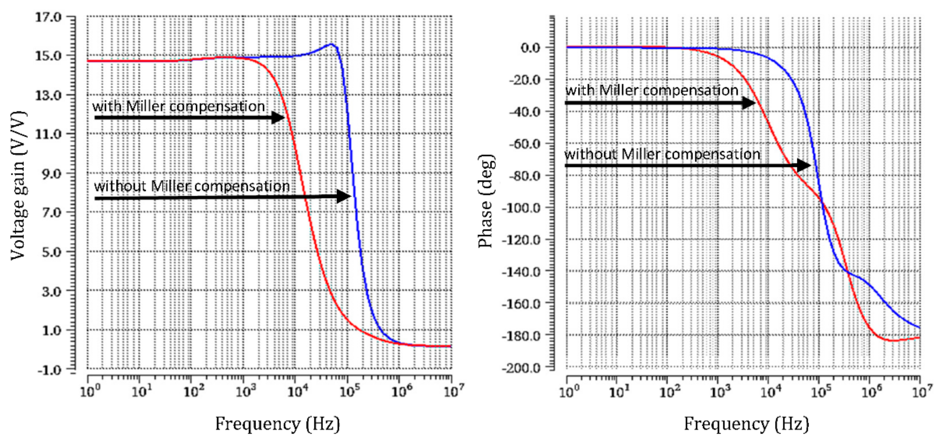
3.3. Frequency Response
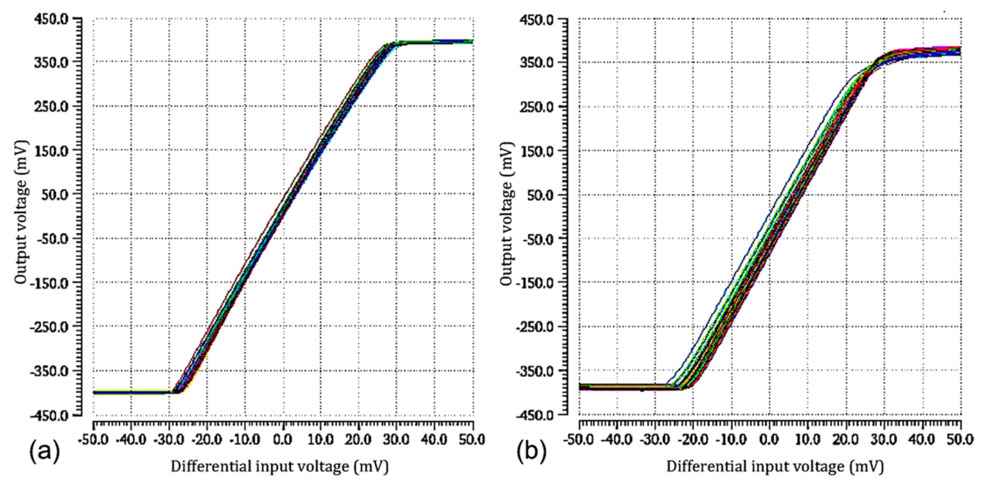
As shown in Section 2, the necessary condition of linearity is that the input transistors must work in a weak inversion region for all combinations of the voltages at the front and back gates. This is acceptable for low power amplifiers, but reduces the achievable bandwidth. An additional problem with the frequency response is that the output resistance of the output stage together with the capacitance of the back gate creates a low pass filter for the feedback signal. As a result, the amplitude of this signal decreases with frequency. This leads to a peak in the frequency response. It can be suppressed by appropriate Miller compensation. This is illustrated in Figure 10.

3.4. Variability

Direct feedback (Figure 3a) may result in a reduction of variability of the amplifier in comparison with the same amplifier with an external feedback loop (Figure 3c). The results of the Monte Carlo simulations of the response of the first amplifier (pre-layout, N = 100, nominal process corner, both process and mismatch variabilities included) are shown in Figure 11. While the nominal responses in both kinds of feedback loop (shown in Figure 5) are almost identical, the variabilities are not. It can be seen (Figure 11) that the statistical spread of the responses of the amplifier with a direct feedback loop (Figure 3a) is noticeably lower than that of the amplifier with an external feedback (Figure 3c).

4. Discussion and Conclusions

As the input differential pair must work in weak inversion (i.e., low drain currents), the linearization technique discussed in this paper is a good technique for low power amplifiers. The first one (Section 3.1) consumes an average of 1 μA only at 0.8 V supply voltage [7]. The second one consumes more: 58 μA at 1.8 V supply voltage. The larger current consumption is as a result of the design of the output stage (Figure 6, larger devices M6A and M7A) and additional current consumption by the voltage divider (Figure 6, devices M8–M10).
The advantages of this linearization technique include a very good linearity and simplicity. There are no additional devices in the case of the direct feedback configuration (Figure 3a), and in particular, no circuit components (e.g., resistors, as in the case of resistive degeneration) connected in series with the transistors in the input stage. As a result, this linearization technique is suitable for low voltage amplifiers. A reduction of variability may be an additional benefit. A voltage divider in the feedback loop (R1–R2, Figure 3b) allows for achieving the desired voltage gain (Equation (5)). These resistors can be either external or on chip. If one of them is variable (e.g., voltage-dependent), a variable gain amplifier is obtained. Of course, attenuation of the feedback signal by the voltage divider reduces the linearity range of the response of the amplifier.
The operating point in the weak inversion of the input pair devices reduces the achievable bandwidth. However, both amplifiers described in this paper were designed as front end amplifiers for the acquisition of biological signals. In this particular application, a bandwidth extending from DC to several kHz is sufficient. As it has been shown in [7], not only linearity, but also low noise, and in particular low flicker noise can be achieved.

Funding

This work was supported by THINGS2DO, an international project co-funded by the European Commission (ENIAC grant agreement 621221) and the Polish National Centre for Research and Development (agreement ENIAC C-2013-2/1/2014).

Conflicts of Interest

The author declares no conflict of interest.

Appendix A

The figures below illustrate the 22 nm FD-SOI chips in which the amplifiers were fabricated. The chips also contain other analog blocks not discussed in this paper. As a reference, the layouts of both chips are shown. Both amplifiers are located in the upper left corners of the chips. The layouts of the amplifiers are not clearly visible on the microphotographs, they are obscured by dummy fills (a.k.a. tiles) that have been added in order to maintain a uniform density of mask shapes on all of the mask layers. This is a technology-related requirement in all nanometer CMOS circuits.
Figure A1. Layouts and microphotographs of the chips in which the amplifiers were fabricated: (a) chip with amplifier 1, chip dimensions 1900 μm × 1400 μm; (b) chip with amplifier 2, chip dimensions 1250 μm × 1250 μm. In both chips, the amplifiers are located in the upper left corners.
Electronics 10 01800 g0a1

References

  1. Cathelin, A. Fully Depleted Silicon on Insulator Devices CMOS: The 28-nm Node Is the Perfect Technology for Analog, RF, mmW, and Mixed-Signal System-on-Chip Integration. IEEE Solid State Circuits Mag. 2017, 9, 18–26. [Google Scholar] [CrossRef]
  2. Planes, N.; Weber, O.; Barral, V.; Haendler, S.; Noblet, D.; Croain, D.; Bocat, M.; Sassoulas, P.-O.; Federspiel, X.; Cros, A.; et al. 28nm FDSOI Technology Platform for High-Speed Low-Voltage Digital Applications. In Proceedings of the 2012 Symposium on VLSI Technology (VLSIT), Honolulu, HI, USA, 12–14 June 2012; pp. 133–134. [Google Scholar]
  3. Nagata, H.; Wada, T.; Ikeda, H.; Arai, Y.; Ohno, M.; Nagase, K. Development of Cryogenic Readout Electronics for Far-Infrared Astronomical Focal Plane Array. IEICE Trans. Commun. 2011, 11, 2952–2960. [Google Scholar] [CrossRef] [Green Version]
  4. Wada, T.; Nagata, H.; Ikeda, H.; Arai, Y.; Ohno, M.; Nagase, K. Development of Low Power Cryogenic Readout Integrated Circuits Using Fully-Depleted-Silicon-on-Insulator CMOS Technology for Far-Infrared Image Sensors. J. Low Temp. Phys. 2012, 167, 602–608. [Google Scholar] [CrossRef]
  5. Ballo, A.; Grasso, A.D.; Pennisi, S.; Venezia, C. High-Frequency Low-Current Second-Order Bandpass Active Filter Topology and Its Design in 28-nm FD-SOI CMOS. J. Low Power Electron. Appl. 2020, 10, 27. [Google Scholar] [CrossRef]
  6. Wołodźko, M.; Kuźmicz, W. A Low Power Input Amplifier for Bio-Signal Acquisition in 28 nm FDSOI Technology. In Proceedings of the 20th IEEE Symposium on Design and Diagnostics of Electronic Circuits and Systems (DDECS), Dresden, Germany, 19–21 April 2017; pp. 79–82. [Google Scholar] [CrossRef]
  7. Kuzmicz, W. A Simple Ultra-Low Power Opamp in 22 nm FDSOI. In Proceedings of the 26th International Conference Mixed Design of Integrated Circuits and Systems (MIXDES), Rzeszów, Poland, 27–29 June 2019; pp. 167–170. [Google Scholar] [CrossRef]
  8. Yang, E.; Lehmann, T. High Gain Operational Amplifiers in 22 nm CMOS. In Proceedings of the 2019 IEEE International Symposium on Circuits and Systems (ISCAS), Sapporo, Japan, 26–29 May 2019. [Google Scholar] [CrossRef]
  9. Harikumar, P.; Wikner, J.J.; Alvandpour, A. An Ultra-Low-Voltage OTA in 28 nm UTBB FDSOI CMOS Using Forward Body Bias. In Proceedings of the 2015 Nordic Circuits and Systems Conference (NORCAS), Oslo, Norway, 26–28 October 2015. [Google Scholar] [CrossRef]
  10. Harikumar, P.; Wikner, J.J.; Alvandpour, A. A Fully-Differential OTA in 28 nm UTBB FDSOI CMOS for PGA Applications. In Proceedings of the 2015 European Conference on Circuit Theory and Design (ECCTD), Trondheim, Norway, 24–26 August 2015. [Google Scholar] [CrossRef]
  11. Jaworski, Z. A fully differential OTA with dynamic offset cancellation in 28 nm FD-SOI process. Proc. SPIE 2016, 10175, 1017509. [Google Scholar] [CrossRef]
  12. Sansen, W. Distortion in elementary transistor circuits. IEEE Trans. Circuits Syst. II Anal. Dig. Signal Proc. 1999, 46, 315–325. [Google Scholar] [CrossRef]
  13. Zhang, H.; Sánchez-Sinencio, E. Linearization Techniques for CMOS Low Noise Amplifiers: A Tutorial. IEEE Trans. Circuits Syst. I Regul. Pap. 2011, 58, 22–36. [Google Scholar] [CrossRef]
  14. Coppejans, P.; Steyaert, M. Dynamic Biasing: A Low Power Linearisation Technique. In Proceedings of the 29th European Solid-State Circuits Conference (ESSCIRC 2004), Estoril, Portugal, 16–18 September 2003; pp. 369–372. [Google Scholar] [CrossRef]
  15. Hernes, B.; Moldsvor, Ø.; Sœther, T. A 80dB HD3 Opamp in 3.3V CMOS Technology using Tail Current Compensation. In Proceedings of the 2001 IEEE International Symposium on Circuits and Systems (ISCAS 2001), Sydney, Australia, 6–9 May 2001; pp. 216–219. [Google Scholar] [CrossRef]
  16. Barbieri, A.; Pernici, S. A Differential Difference Amplifier with Dynamic Resistive Degeneration for MEMS Microphones. In Proceedings of the 42nd European Solid-State Circuits Conference (ESSCIRC 2016), Lausanne, Switzerland, 12–15 September 2016; pp. 285–288. [Google Scholar] [CrossRef]
  17. Popa, C.; Coada, D. A New Linearization Technique for a CMOS Differential Amplifier Using Bulk-Driven Weak Inversion MOS Transistors. In Proceedings of the International Symposium on Signals, Circuits and Systems (SCS 2003), Iasi, Romania, 10–11 July 2003; pp. 589–592. [Google Scholar] [CrossRef]
  18. Yodtean, A.; Isarasena, P.; Thanachayanont, A. 0.8-µW CMOS Bulk-Driven Linear Operational Transconductance Amplifier in 0.35-µm Technology. In Proceedings of the 2010 IEEE Asia Pacific Conference on Circuits and Systems, Kuala Lumpur, Malaysia, 6–9 December 2010; pp. 784–787. [Google Scholar] [CrossRef]
  19. Zhang, L.; Zhang, X.; El-Masry, E.; Zhang, Y. A Low-Voltage High Linear Body-Driven Operational Transconductance Amplifier and Its Applications. In Proceedings of the 2007 Canadian Conference on Electrical and Computer Engineering, Vancouver, BC, Canada, 22–26 April 2007; pp. 534–537. [Google Scholar] [CrossRef]
  20. El Ghouli, S.; Rideau, D.; Monsieur, F.; Scheer, P.; Gouget, G.; Juge, A.; Poiroux, T.; Sallese, J.-M.; Lallement, C. Experimental gm/ID Invariance Assessment for Asymmetric Double-Gate FDSOI MOSFET. IEEE Trans. Electron. Devices 2018, 65, 11–18. [Google Scholar] [CrossRef]
  21. Khateb, F.; Biolek, D.; Khatib, N.; Vávra, J. Utilizing the Bulk-driven Technique in Analog Circuit Design. In Proceedings of the 13th IEEE Symposium on Design and Diagnostics of Electronic Circuits and Systems (DDECS), Vienna, Austria, 14–16 April 2010; pp. 16–19. [Google Scholar] [CrossRef]
  22. Carrillo, J.M.; Duque-Carrillo, J.F.; Torelli, G. Design Considerations on CMOS Bulk-Driven Differential Input Stages. In Proceedings of the 2012 International Conference on Synthesis, Modeling, Analysis and Simulation Methods and Applications to Circuit Design (SMACD), Seville, Spain, 19–21 September 2012; pp. 85–88. [Google Scholar] [CrossRef]
  23. Grech, I.; Micallef, I.; Azzopardi, G.; Debono, C.J. A low-voltage wide-input-range bulk-input CMOS OTA. Analog Integr. Circ. Signal Process. 2005, 43, 127–136. [Google Scholar] [CrossRef]
  24. Raikos, G.; Vlassis, S. 0.8 V Bulk-Driven Variable Gain Amplifier. In Proceedings of the 17th IEEE International Conference on Electronics, Circuits and Systems, Athens, Greece, 12–15 December 2010; pp. 343–346. [Google Scholar] [CrossRef]
  25. Tai, C.-F.; Lai, J.-L.; Chen, R.-J. Using Bulk-driven Technology Operate in Subthreshold Region to Design a Low Voltage and Low Current Operational Amplifier. In Proceedings of the 2006 IEEE International Symposium on Consumer Electronics, Saint Petersburg, Russia, 28 June–1 July 2006; pp. 562–566. [Google Scholar] [CrossRef]
  26. Rakús, M.; Stopjaková, V.; Daniel, A. Analysis of Bulk-Driven Technique for Low-Voltage IC Design in 130 nm CMOS Technology. In Proceedings of the 15th International Conference on Emerging eLearning Technologies and Applications (ICETA), Starý Smokovec, Slovakia, 26–27 October 2017; pp. 385–390. [Google Scholar] [CrossRef]
Figure 1. NMOS device located over an isolated P-well. “Hybrid” regions are regions where the BOX is removed and serve as contact areas to the N-wells and P-wells.
Electronics 10 01800 g001
Figure 2. The concept of the linearization technique: output voltage between the output and the virtual ground is applied between the back gates of the input differential pair.
Electronics 10 01800 g002
Figure 3. Three configurations of the amplifiers: (a) direct feedback (as in Figure 2), (b) feedback with voltage divider, (c) and external linear negative feedback.
Electronics 10 01800 g003
Figure 4. The first amplifier [7].
Electronics 10 01800 g004
Figure 5. Simulated in two configurations (a) and measured in the direct feedback configuration, and the (b) response of the first amplifier.
Electronics 10 01800 g005
Figure 6. The second amplifier. The input stage is the same as in the first one, see Figure 4.
Electronics 10 01800 g006
Figure 7. Layout of the second amplifier. Layout dimensions: 215.3 μm × 120 μm. The microphotographs of chips with both amplifiers are shown in Appendix A.
Electronics 10 01800 g007
Figure 8. Simulated in two configurations (a) and measured in the direct feedback configuration, and (b) response of the second amplifier.
Electronics 10 01800 g008
Figure 9. Simulated (a) and measured (b) response of the second amplifier in the configuration with a voltage divider in the feedback loop (Figure 3b, R1 = 9.4 MΩ, R2 = 4.7 MΩ).
Electronics 10 01800 g009
Figure 10. Simulated frequency response (voltage gain and phase) of the first amplifier (Figure 4) with Miller compensation and without it.
Electronics 10 01800 g010
Figure 11. Results of Monte Carlo simulation of the response of the first amplifier in the direct feedback loop configuration (a) and external feedback loop configuration. (b) Both process and mismatch statistical variations are included.
Electronics 10 01800 g011
Publisher’s Note: MDPI stays neutral with regard to jurisdictional claims in published maps and institutional affiliations.

