Abstract
In the era of the Internet of Things (IoT), the interest and demand for embedded systems have been explosively increasing. In particular, vehicular sensor networks are one of the fields where IoT-oriented embedded devices (also known as IoT devices) are being actively used. These IoT devices are widely deployed in and out of the vehicle to check vehicle conditions, prevent accidents, and support autonomous driving, forming a vehicular sensor network. In particular, such sensor networks mainly consist of third-party devices that operate independently of the vehicle and run on their own batteries. After all, like all battery-powered embedded devices, the IoT devices for the vehicular sensor network also suffer from limited power sources, and thus research on how to design/operate them energy-efficiently is drawing attention from both academia and industry. This paper notes that the vehicular sensor network may be the best application for ultra-low power system on-chips (ULP SoCs). The ULP SoCs are mainly designed based on ultra-low voltage operating (ULV) circuits, and this paper aims to realize the energy-optimized driving of the network by applying state of the art (SoA) low-power techniques exploiting the unique characteristics of ULV circuits to the IoT devices in the vehicular sensor network. To this end, this paper proposes an optimal task assignment algorithm that can achieve the best energy-efficient drive of the target network by fully utilizing the SoA low power techniques for ULV circuits. Along with a detailed description of the proposed algorithm, this paper demonstrates the effectiveness of the proposed method by providing an in-depth evaluation process and experimental results for the proposed algorithm.
1. Introduction
As Internet of Things (IoT) has grown significantly, numerous sensors and embedded systems have been developed explosively and are being released as IoT devices [1,2,3]. One of the areas where IoT market trends are most prominent is the automotive industry. Vehicles that are transforming into a second main living space following customers’ homes are using various auxiliary systems for safety and security as well as various conveniences. Some of these auxiliary systems have been produced by vehicle manufacturers and are already deployed to the vehicle during the vehicle manufacturing phase. Unfortunately, however, vehicle manufacturers cannot satisfy all the needs of a wide variety of customers, so a variety of third-party products are emerging to meet them.
Third-party IoT devices for vehicles are fitted to various places in the vehicle for various purposes, forming a single independent sensor network. These devices operate separately from the vehicle’s engine control unit (ECU) and are powered by their own internal battery rather than by the power source in a vehicle. Therefore, they cannot be free from the inconvenience of charging, the biggest issue of battery-powered devices, which means how long they can be used on a single charge is the most important factor in determining their usefulness.
In this study, we conducted a study on the development of an ultra-efficient sensor network consisting of third-party IoT devices for vehicles. Of the various vehicular sensor networks, we targeted a network consisting of sensing units (called motes) that collect data through sensors and devices (called processing nodes) that receive and process data from the motes and send them to a base station, as shown in Figure 1. In particular, we studied how to develop the most energy-efficient processing nodes, as nodes may be the most power-hungry devices in the network. To this end, we first focused on ultra-low power (ULP) system-on-chips (SoCs). The ULP SoCs are designed primarily based on ultra-low voltage (ULV) operating circuits and consume up to tens of times less power than conventional SoCs operating with nominal supply voltage [4,5,6,7,8]. Of course, these ULP SoCs have the disadvantage of significant performance degradation compared to conventional SoCs (i.e., their clock frequency may be less than just tens of MHz [9]). However, considering that the computing capability required by our target processing nodes for the in-vehicle sensor network is not that high, and ULP SoC ultra-low power can significantly increase the life of the device, utilizing such ULP SoCs for the processing nodes may be the most suitable solution.
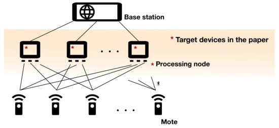
Figure 1.
The target vehicular sensor network: the motes collect data and send them to the processing nodes. Each processing node processes the tasks assigned from the motes and sends the result to the base station. It is supposed that both the motes and processing nodes are distributed in different locations on the vehicle.
Next, we turned our attention to the recent studies that have shown that the ULP SoCs have very specific characteristics compared to nominal voltage operating SoCs: the ULP SoCs speed up as temperatures rise [10,11]. This phenomenon is called temperature effect inversion (TEI) [12], and a variety of state of the art low-power techniques have been published exploiting it [9,12,13,14,15,16,17,18,19,20,21,22]. More precisely, TEI-aware voltage scaling (TEI-VS) techniques saved power without performance degradation of SoCs [9,12,13,14,15], TEI-aware frequency upscaling (TEI-FS) showed that SoCs can operate in turbo mode with a linear increase in power consumption (and thus a very small increase in power consumption compared to the existing one) [16,17,23], and TEI-aware body biasing (TEI-BB) demonstrated that the low power potential utilizing the TEI phenomenon can be realized by further complementing TEI-VS and FS techniques [18,19]. In addition, recent research has confirmed the effectiveness of these methods on fabricated system-on-chips (SoCs) [9,20,21,22].
We then investigated the temperature distribution of various parts of a vehicle to determine whether our target environment is suitable for utilizing the TEI-aware low power techniques. Figure 2 shows the temperature distribution for each part of our target SUV vehicle. Since the processing nodes are distributed in various places in the vehicle, the sensor network we are targeting can be expected to have different temperatures depending on the location where the devices are attached. That is, since the processing nodes have different temperatures, they have different performance and power consumption/energy efficiency. Considering that this condition is the environment where the effectiveness of the TEI-aware low power techniques is expected the most, we decided to actively utilize TEI-aware low power techniques. Then, to determine which of the various TEI-aware low power techniques will be most viable for our target system, we focused on the other important design factors of the target devices, design complexity and fabrication cost. TEI-VS and TEI-BB require a DC–DC converter and a body biasing controller, respectively, which increases the chip area and development cost of the SoC. By contrast, TEI-FS requires only the addition of a simple phase-locked loop (PLL) logic, which is advantageous in terms of area and cost. Therefore, we determined that TEI-FS is the most appropriate method for our target application, and decided to utilize this technique in this paper.
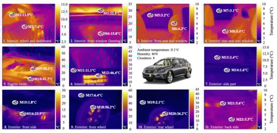
Figure 2.
An example of the thermal distribution of a car: the car is divided into 11 parts and each thermal image of the part is taken with an infrared camera. The weather condition is reported in the middle of the figure, and each image includes the temperature information of two specific spots.
Finally, to realize the most energy-efficient operation of the sensor network of the vehicle configured with ULP SoC-based processing nodes, we defined the following problem: There are processing nodes that vary in energy efficiency depending on temperature, which share and process tasks given by motes. Then, we ask: Which processing node each task is assigned to, and at what speed each processing node operates, is the most energy-efficient way to finish all tasks in a given time? To solve this problem, we propose an optimization algorithm that can perform optimal task distribution while leveraging TEI-FS. In addition, in this paper, we demonstrate the superiority of algorithms based on real SoCs by performing performance evaluations of algorithms using the IoT devices built with the ULP SoCs.
The remainder of this paper is organized as follows. Section 2 elucidates the details of the TEI phenomenon and existing TEI-aware low power techniques including TEI-FS. Section 3 introduces the proposed task distribution algorithm utilizing TEI-FS for the vehicular sensor network. Next in Section 4, we perform the evaluation by using the ULP SoC that we made. Finally, Section 5 concludes the paper.
2. TEI-Aware Low Power Techniques: A Preliminary
The delay of a transistor in a circuit is directly affected by the on-current of the transistor such that , where C denotes the load capacitance of the transistor, and is the supply voltage. As increases, the transistor switches faster, and vice versa. Therefore, to analyze the TEI phenomenon, we first explore the theoretical model of . as a function of the circuit temperature T can be expressed as:
where is the gate-source voltage, S denotes the subthreshold swing coefficient (also known as the body effect coefficient), is the carrier mobility, and represents the velocity saturation effect factor (a typical value for is 1.45.) S, , and are temperature-dependent device parameters. When we first consider a transistors whereby T increases, and both decrease while S increases. In (1), when the transistor operates in the super-threshold voltage regime (i.e., ), is mainly affected by (although somewhat mitigates the effect of changes). Consequently, decreases as T rises, which is the well-known negative relationship between and T. Therefore, the worst-case timing corner for the commercial CMOS standard cell libraries operating in the superthreshold voltage regime occurs at the highest operating temperature. On the other hand, in (2), when the transistor operates in the ULV regime, and S have an exponential and dominant influence on , and the combined effect shows a significantly increased as T rises [10]. This is called the TEI phenomenon [12]. In other words, circuits containing ULV operating transistors tend to become faster at higher temperatures. Figure 3 shows the TEI phenomenon in both CMOS and FinFET-based circuits. The figure is generated based on circuit simulations performed with a 55 nm DDC technology library and 20 nm/14 nm FinFET PTM libraries [24], each of which clearly shows that the delay decreases with rising temperature.
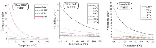
Figure 3.
TEI phenomenons in 55 nm CMOS-based circuit and 20 nm/14 nm FinFET-based circuits.
The TEI-aware low power techniques actively exploit the TEI phenomenon to achieve the energy-efficient improvements. To theoretically analyze the characteristics and effects of each of these techniques, we first describe the power consumption of a circuit as follows [12,16]:
where , , f and are the activity factor, supply voltage, operating frequency, and off-current of the circuit, respectively. Now, we focus on the best known TEI-aware low power technique, TEI-VS, that is based on the fact that the reference and f of the circuit are determined at the lowest temperature at which the worst case corner of the ULV operating circuit is. TEI-VS supplies circuits with the lowest that satisfies the target f at a given temperature, based on the idea that a voltage lower than the reference voltage (due to the TEI phenomenon) can be used. As in (3), lowering has great effects on both and . Figure 4 illustrates the effectiveness of TEI-VS. For example, Figure 4a shows the TEI phenomenon from the simulation with FO4 inverter chain based on CMOS 40n LP technology, while Figure 4b shows the resulting power consumption of the circuit with various and T. Note that the values in both figures are normalized. As seen from the figures, when the target f is determined by a 0.5 V supply at −15 °C, can be reduced to 0.45, 0.40, and 0.35 V as the higher T’s, which in turn saves power.
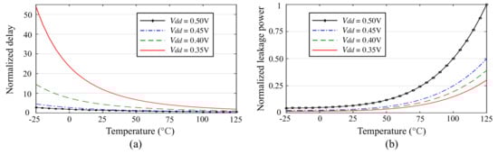
Figure 4.
Simulation results of the FO4 inverter chain based on CMOS 40n LP process library: (a) normalized delay and (b) normalized leakage power consumption under a wide range of temperature values. The normalizations were carried out based on V at 125 °C.
TEI-BB is a technique used to change the threshold voltage () by adjusting the body voltage of the transistors and control the speed and power consumption of the circuit through this. Compared to TEI-VS, TEI-BB has the same principle of achieving power saving, except that the latter changes Vdd and the former changes the body voltage.
Meanwhile, TEI-FS focuses on f values that can scale up without upscaling at the high T. Compared to the conventional turbo-mode, where upscaling is required to operate the circuit at a higher frequency than reference f, thereby in (3) cubically increases, TEI-FS can only increase f without upscaling at a given T, resulting in a linear increase in and no change in . Compared to the TEI-VS
and TEI-BB that require a DC–DC converter(s) inducing area and cost overheads [17,25,26], TEI-FS requires a simple PLL controller that is relatively easy to develop and has a small form factor on the chip. Therefore, considering that our target SoCs for the vehicular sensor network need to be simple, economical, and easy to develop, in this paper we attempt to use TEI-FS for the target application.
3. TEI-Aware Task Assignment
As noticed in (3), when the frequency is scaled according to voltage scaling, behaves as a cubic function of . However, becomes a nearly linear function of , because other effects, such as drain induced barrier lower (DIBL), are very insignificant [27,28]. As becomes smaller into the ULV regime, becomes a major contributor to the total power consumption of ULP devices (i.e., the processing nodes in this paper). Motivated by this fact, we focus on the power-gating (PG) technique, which saves power by shutting down power when the circuit is not working. This technique is one of the most powerful dynamic power management techniques used to reduce leakage power, and may be particularly effective in ULP SoCs, where leakage power accounts for a very large proportion of the total power consumption.
We then propose an idea that utilizes TEI-FS. More in detail, we propose a power gating and frequency upscaling (PGFS) technique that upscales the frequency (i.e., turbo-mode) of a device (i.e., processing node) at a certain high temperature and turns off some devices at low temperature. From this PGFS technique, the performance of the network can be maintained because the turbo-mode device takes over the tasks that were originally assigned to the turned-off devices and processes them in time. At the same time, the total power consumption of the network can be saved from the turned-off devices. More precisely, the amount of power saving from the power gated devices may be greater than the amount of power increase due to the frequency upscaled devices. Again, this can be achieved, because TEI-FS does not need to scale up but increases linearly.
To elaborate on the proposed idea, we consider situations in which there are three devices and three tasks in the vehicular sensor network. Each device operates at the default frequency that is determined by the worst-case corner (i.e., the lowest temperature) of the device. In other words, all of the devices should operate at least at to guarantee the normal operation. When we suppose that is 100 MHz, the required frequencies of the devices to complete the given tasks in time are 25, 30, and 50 MHz. In this situation, the conventional task assignment policy that evenly distributes the tasks to the three devices must not be optimal from the power saving perspective. Instead, using two devices and turning off one device, for instance, by assigning 25 and 30 MHz to one device and 50 MHz to another device, should be better to save power. Then, we are faced with the problem of which device to turn off. If TEI-FS is not enabled in the devices, the device at the highest temperature among the three devices must be turned off, because it consumes the highest leakage power (i.e., is a function of temperature).
Then, when TEI-FS is taken into account, the optimal solution of the given situation must be changed. For example, assuming that one of the devices is at 50 °C, and this device can thus operate up to 200 MHz without voltage scaling, it would be better to assign all of the tasks to the device at the highest temperature, make it operate at 105 MHz, and turn off the others. Next, if we assume there is another device at 40 °C, thereby it can operate up to 150 MHz, it should be better to assign all of the tasks to this device and make its frequency 105 MHz, instead of using the device at 50 °C.
Although the above example is straightforward, assigning tasks to the devices at various temperatures and applying the proposed PGFS technique to the devices is combinatorially very challenging. To address this problem, we focus on the dynamic task assignment of the target vehicular sensor network, which aims to optimally configure the network between the tasks and devices for each certain time period D, so that the total power consumption of the devices should be minimized for D. Then, we assume that there are N devices, each of which has its own range of the operating frequency f. According to the given temperature T, the possible frequency range can be expressed as , where is same for all devices, whereas is the maximum possible frequency of the device that is determined at the current temperature of the device. In addition, we assume that there are M tasks with the required operating frequencies, ,…,. Finally, we face a combinatorial problem with the objective to minimize the overall power consumption of the devices by optimally assigning the tasks to the devices, determining the frequency of each device, and turning off the devices that do not have any assigned tasks. We formally describe the problem as follows:
where and are the power consumption and operating frequency of the device, respectively; is the required frequency of the processing node of the task to complete the task in a given time, and is the set of tasks that are assigned to the device, whereby are mutually exclusive. In the problem, we set assumptions as follows: (i) D is set to be longer enough relative to the breakeven-time in the power gating, so that the energy loss from the power gating becomes negligible, and (ii) is not changed in D (i.e., in general, device temperature changes very slowly).
The problem is NP-hard. To prove the NP hardness of the problem, we can reduce the problem by setting ; then the problem is transformed to a variable bin packing problem. However, setting to can cause critical errors in the original problem in that devices with always waste computing power. Therefore, we cannot fix to and apply algorithms for the variable bin packing problem.
To solve the problem, we propose an algorithm described in Algorithm 1: TEI-aware dynamic task assignment (TEI-DTA). In the algorithm, we first pay attention to the fact that if all the devices operate at , using the devices in the low temperature regime should be preferred because such devices consume less . We therefore fix all to and assign the tasks to the devices in ascending order of (cf. lines 2 to 5 in Algorithm 1). The -- (FFD) algorithm for a bin packing problem is used in this task assignment. We sort all s in descending order (cf. lines at 6 in Algorithm 1), and perform the first-fit function, Do_FF, to initially assign the tasks to the devices (cf. line 10 in Algorithm 1). The details of Do_FF are elucidated in Algorithm 2, whereby it returns the ordered set of the used devices . Note that we define such a set of the used devices and an ordered set of its index K, and k is the maximum value of K (cf. lines at 7 and 8 in Algorithm 1).
| Algorithm 1 TEI-aware dynamic task assignment algorithm. | ||
| 1: | procedureDo_TEI_Aware_Task_Assingment | |
| 2: | for do | |
| 3: | , | ▹ Initialization |
| 4: | end for | |
| 5: | Sort , in ascending order of the corresponding using Counting Sort, so that . | |
| 6: | Sort , in descending order using Counting Sort, so that . | |
| 7: | Define is the ordered set of the processing nodes that are used, and is the associate total power . | |
| 8: | Define is the ordered set of and k is the maximum value of K. | |
| 9: | Define is the potential power saving of , whereby . and can be estimated from a power model based on (3) or pre-measured data in a LUT. | |
| 10: | Do_FF(, {1,…,M}, M, N) | ▹ Do_FF is presented in Algorithm 2. |
| 11: | is the ascending ordered set of t satisfying . | |
| 12: | If empty, stop the procedure. Otherwise, go to the next. | |
| 13: | for do | |
| 14: | ||
| 15: | ||
| 16: | ||
| 17: | Do_DP() | ▹ Do_DP is presented in Algorithm 3. |
| 18: | if then | |
| 19: | ▹ Increase by . | |
| 20: | ▹ Update . | |
| 21: | , | ▹ Consolidation. |
| 22: | Add to . Delete ’s () from . Update K from . | ▹ Update and K. |
| 23: | Add to at the last sequentially. | ▹ Extend . |
| 24: | end if | |
| 25: | end for | |
| 26: | end procedure | |
| Algorithm 2 First-fit algorithm for the initial packing. | ||
| 1: | functionDo_FF(, , M, N) | |
| 2: | is the corresponding frequency of in . | |
| 3: | is the corresponding frequency of j motes in . | |
| 4: | for do | |
| 5: | for do | |
| 6: | if then | ▹ if fits in device, |
| 7: | , | ▹ Assign j in i. |
| 8: | Break | ▹ Break the loop and pack the next. |
| 9: | end if | |
| 10: | end for | |
| 11: | end for | |
| 12: | return an ordered set of ’s, if , | |
| 13: | end function | |
| Algorithm 3 Dynamic programing for the consolidation. | ||
| 1: | functionDo_DP(v,w,s,K,W) | |
| 2: | for do | |
| 3: | end for | |
| 4: | for do | |
| 5: | for do | |
| 6: | if then | |
| 7: | max, | |
| 8: | else | |
| 9: | end if | |
| 10: | end for | |
| 11: | end for | ▹ is the maximum value. |
| 12: | ||
| 13: | while do | ▹ This is to find the used items. |
| 14: | if then | |
| 15: | , , | |
| 16: | else | |
| 17: | end if | |
| 18: | end while | |
| 19: | return , , S | |
| 20: | end function | |
Next, we try to consolidate to the smaller number of devices that are in a high temperature regime, so as to exploit the PGFS technique to save power. In other words, if there are devices that can operate with , so that these devices may be affordable to take over and process any task assigned to another devices, we apply these devices to a set of consolidation acceptors, , in the ascending order of the temperature (cf. line at 11 in Algorithm 1). Then, we investigate whether the consolidation to the device results in power saving. If is empty, each device does not have space to expropriate the task from the other devices. Hence, there is no more work to proceed. Otherwise, the task reallocation is possible and the algorithm goes to the next step for comparing the power consumption saving (cf. line at 12 in Algorithm 1). To do that, let us define to denote the target device with t in and to denote the potential power savings of from being consolidated to . Note that equals to as shown in lines 9 in Algorithm 1.
As we treat and , as value and weight, respectively, the problem to select s to maximize while satisfying can be transformed into a 0–1 . We adopt a dynamic programming algorithm that is a well-known solution of the 0-1 knapsack problem. In line 17 in Algorithm 1, we perform a function Do_DP that is based on the dynamic programming algorithm. The details of the function Do_DP are described in Algorithm 3, whereby this function returns the maximum power saving values, the sum of the required frequency for processing tasks, and the list of the consolidated devices, each of which are saved in , , and , respectively, in Algorithm 1. Finally, the comparison between and the increasing power from the reallocated list of tasks that consists of both dynamic power and leakage power is performed, as shown in line 18 in Algorithm 1. If the former is larger than the latter, which means the consolidation saves power, we should set to be , and to be , and then set to be ∅ and update by adding and deleting . Then, obviously, we should refresh K through the reallocated and update by adding (cf. line at 19 to 22 in Algorithm 1). Otherwise, we do not perform any consolidation to . Additionally, in line 23 in Algorithm 1, is extended by adding at the last sequentially to reinforce our procedure, which means repeating the proceeds of the loop (i.e., lines 14 to 24 in Algorithm 1) only for consolidated devices.
The above consolidation procedure is performed for all devices that can accept an additional task (i.e., ) and the accompanying s are kept updated until the end of the procedure. Finally, the final provides the information regarding which devices should be turned on or off, where to assign the task of each device, and how to set up the frequency of each turned-on device. Additionally, defined in line 7 in Algorithm 1 yields the total power consumption of the final .
Applying the proposed algorithm to a device, i.e., a processing node in this paper, may require additional hardware support. For example, a temperature sensor to check the temperature changes in the device [29] or a ring-oscillator-based performance monitoring logic to determine the circuit speed [30] may be necessary to perform the frequency scaling at runtime. In addition, since the algorithm utilizes and , there should be a way to estimate these values. To this end, as a software-based approach, a power model based on (3) can be exploited [31], or as a hardware-based approach, a look-up table (LUT) storing pre-measured and values for all cases can be adopted [32]. In this study, we mounted an on-board temperature sensor on the prototype of the processing node and measured the power consumption of this prototype device at various temperatures through experiments. However, the functionality and effectiveness verification of the proposed algorithm was derived through simulations using the measured above data. A detailed description of the experimental work is provided in the following chapter.
4. Experimental work
4.1. Experimental Setup
To evaluate the effectiveness of the proposed TEI-DTA algorithm, we first attempted to acquire TEI-FS data measured from the target IoT devices. To do that, we utilized our TEI-inspired SoC platform (TIP) [8] and the TIP prototyping SoC operating with 50 MHz operating frequency at 0.7 V supply [9]. More in detail, the TIP is configured with dual RISC-V (ORCA) cores, micro network-on-chip (NoC), and peripherals, with a detailed architecture illustrated in Figure 5. Based on the TIP, the ULP SoC prototype was fabricated using 28 nm FDSOI technology, and the die photo of this SoC prototype is shown in Figure 6a. Then, by embedding the SoC prototype into the test board that has an on-board temperature sensor and a programmable oscillator to enable adjustment of the of the chip clock frequency at run time, the processing node prototype for the target sensor network was established, which is described in Figure 6b. Finally, we placed this prototype in an environmental test chamber, as shown in Figure 7, and measured the TEI-FS effect of the devices by changing the temperature of the devices. From this experimental work, we first checked that in room temperature (25 °C), the device can maintain its operating frequency (50 MHz) at a 0.48 V supply, which is much lower than the nominal voltage of 0.7 V, and from this, we confirmed that the TEI phenomenon is evident on this device. Next, using that condition as a reference, we measured the maximum operating frequency for each temperature of the device when the supply voltage was fixed at 0.48 V, and the result is shown in Figure 8. From these experiments, we obtained data that the target device operated at 20 MHz at −10 °C, but with increasing temperatures, it operated at 40 MHz at 10 °C, 60 MHz at 45 °C, and 75 MHz at 80 °C without any change in supply voltage. These data and the corresponding power consumption measured at each circumstance point, as also shown in Figure 8, were utilized as resources during the TEI-DTA algorithm evaluation process.
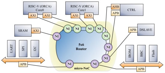
Figure 5.
Architecture of the TEI-inspired SoC platform used for our target ULP SoC. In the figure, APB, AHB, and AXI are AMBA protocols, NI, and CTRL, respectively, representing the network interface and controller, and the rest are typical peripherals.
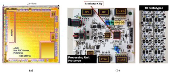
Figure 6.
(a) Silicon Die photo of the prototyping SoC, and (b) the IoT device boards with the prototyping SoCs (sourced from [9]).
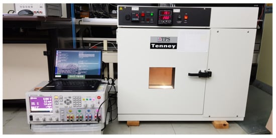
Figure 7.
The experimental environment used to test the TEI phenomenon of the devices (sourced from [9]).
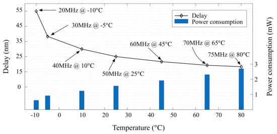
Figure 8.
Measured result of scalable frequency and corresponding power consumption of the prototyping processing unit at each temperature point when TEI-FS is employed and = 0.48 V.
4.2. Evaluation of the TEI-DTA Algorithm
To demonstrate the superiority of the proposed TEI-DTA algorithm, we first defined a metric that represents how much power consumption improves when TEI-DTA is applied over the total power consumption of the existing sensor network, which is:
where is the power saving ratio, and and are the power consumed when task assignment is not specifically configured and after configuration with TEI-DTA, respectively. Then, we set both M and N in the TEI-DTA algorithm to 22, which is based on the target sensor network configuration described in Figure 2. During the evaluations, the power consumption of each processing unit was derived based on data measured by placing the processing unit prototype in a chamber and varying the temperature and operating frequency.
For the initial evaluation of the proposed TEI-DTA in the vehicular sensor networks, we set the operating temperature range of devices from to 80 °C. We also defined , which is a minimum operating frequency that ensures that the required frequency of the processing unit for the task is limited to less than this frequency. Then, we carried out a Monte Carlo simulation with five different group of tasks, each of whose required frequency average of the tasks is 30%, 40%, 50%, 60%, and 70% for , as described in Figure 9. As shown in the figures and the following Table 1 that reports the results in detail, the TEI-DTA algorithm achieved power savings in every condition of the simulation. When the required frequency was 30%, the average power saving ratio achieved up to 76.5%, and when the required frequency was reduced, it decreased to 65.7%, 56.5%, 46.3%, and 37.9%, respectively. These results imply that the smaller the sizes of tasks, the greater the power gain of our method. This is due to the fact that the smaller the task, the more tasks can occupy one device, which increases the number of power-gated devices, resulting in a lower total leakage power in the network.
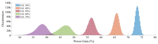
Figure 9.
Monte Carlo simulation results of the power gain for each required frequency.

Table 1.
Average and extreme values of for each required frequency.
We demonstrated through initial experiments that TEI-DTA can save power at a wide range of operating temperatures, followed by experiments to demonstrate the effectiveness of TEI-DTA in more practical situations. To this end, we conducted five real-world case studies, including the real-world vehicle environment in Figure 2. We have already analyzed the impact of the required frequency average of the tasks on power saving through previous experiments, so in these case studies, we fixed the required frequency average of the tasks at 70%. For Case #1, the measured conditions in cold weather in Figure 2 were utilized. Case #2 represents a hot weather device operating environment, which is the opposite of Case #1. In addition, we set Cases #3, #4, and #5 to be under operating environments at low ( °C), middle ( °C), and high ( °C) temperature ranges, respectively.
100,000 Monte Carlo simulations were performed by applying the proposed TEI-DTA for each case, and finally Table 2 reports the average result value () for each case. As can be seen from the table, the effectiveness of TEI-DTA in Case #1 achieved a 52.5% power consumption improvement, and that in Case #2 increased further to 55.8%. In addition, by analyzing the results in Cases #3, #4, and #5, we could confirm that the of the TEI-DTA grows when devices in the network are in a high-temperature environment (the average reached up to 61.6%), while is relatively low at low temperature, but the effect remains excellent (49%).
Table 2.
Average results for the case studies.
5. Conclusions
In this paper, we noted that while the demand for vehicular sensor networks based on third-party IoT devices is continuously increasing, development is being delayed due to the limitation that these IoT devices must be operated with limited power sources. To address this problem, we focused on the ULP SoCs based on ULV operating circuits, which are best suited for energy-efficient vehicle sensor networks. In particular, we paid attention to the special characteristics of these ULP SoCs, i.e., operating speed increases as the temperature rises due to the TEI phenomenon, and explored the latest low-power techniques, i.e., TEI-aware low power techniques, exploiting these characteristics. Among the various TEI-aware low-power techniques, we determined that TEI-FS is the most suitable for the target sensor network, and devised a method to drive the sensor network with the highest energy efficiency by unleashing the full potential of TEI-FS. To this end, we proposed an optimal task assignment algorithm called TEI-DTA. Along with the detailed description of the proposed algorithm, an in-depth evaluation process for the fabricated SoC and intensive experimental work based on the measured data were performed to evaluate the effectiveness of this algorithm. As a result, the proposed algorithm achieved a significant power consumption reduction effect in the target vehicular sensor network. We expect that the proposed algorithm and demonstration will be utilized as a low-power technology in IoT applications with distinct temperature distribution such as the vehicular sensor network targeted in this paper.
Author Contributions
S.-Y.L., J.-H.L., J.L. and W.L. were the main researchers who initiated and organized research reported in the paper, and all authors were responsible for analyzing the simulation results and writing the paper. All authors have read and agreed to the published version of the manuscript.
Funding
This research was partially supported by the Chung-Ang University Research Scholarship Grants in 2019, and partially supported by the National R&D Program through the National Research Foundation of Korea (NRF) funded by Ministry of Science and ICT (2021M3H2A1038042).
Data Availability Statement
The data presented in this study are available on request from the corresponding author.
Conflicts of Interest
The authors declare no conflict of interest.
References
- Petrov, V.; Samuylov, A.; Begishev, V.; Moltchanov, D.; Andreev, S.; Samouylov, K.; Koucheryavy, Y. Vehicle-Based Relay Assistance for Opportunistic Crowdsensing Over Narrowband IoT (NB-IoT). IEEE Internet Things J. 2018, 5, 3710–3723. [Google Scholar] [CrossRef]
- Lee, S.Y.; Lee, J.H.; Jang, H.; Lee, W. A Framework for Detecting the Presence of an Unattended Child in a Vehicle. In Proceedings of the 2020 International SoC Design Conference (ISOCC), Yeosu, Korea, 21–24 October 2020; pp. 59–60. [Google Scholar]
- Borges, V.E.F.C.; Santos, D.F.S.; Perkusich, A.; Malarski, K.M. Survey and Evaluation of Internet of Vehicles Connectivity Challenges. In Proceedings of the 2020 International Conference on Software, Telecommunications and Computer Networks (SoftCOM), Split, Croatia, 17–19 September 2020; pp. 1–6. [Google Scholar]
- Gautschi, M.; Schiavone, P.D.; Member, S.; Traber, A.; Loi, I.; Pullini, A.; Rossi, D.; Flamand, E.; Gürkaynak, F.K.; Benini, L. Near-threshold RISC-V core with DSP extensions for scalable IoT endpoint devices. IEEE Trans. Large Scale Integr. Syst. 2017, 25, 2700–2713. [Google Scholar] [CrossRef] [Green Version]
- Karnik, T.; Kurian, D.; Aseron, P.; Dorrance, R.; Alpman, E.; Nicoara, A.; Popov, R.; Azarenkov, L.; Moiseev, M.; Zhao, L.; et al. A cm-scale self-powered intelligent and secure IoT edge mote featuring an ultra-low-power SoC in 14 nm tri-gate CMOS. In Proceedings of the International Solid-State Circuits Conference Digest of Technical Papers, San Francisco, CA, USA, 11–15 February 2018; pp. 46–48. [Google Scholar]
- Pu, Y.; Shi, C.; Samson, G.; Park, D.; Beraha, R.; Newham, A.; Lin, M.; Rangan, V.; Chatha, K.; Butterfield, D.; et al. A 9-mm2 ultra-low-power highly integrated 28-nm CMOS SoC for internet of things. IEEE J. Solid-State Circuits 2018, 53, 936–948. [Google Scholar] [CrossRef]
- Hwang, W.; Yoo, K.; Thai, D.V.; Lee, W.; Baek, K.H. Design of a DC–DC Converter Customized for Ultra-Low Voltage Operating IoT Platforms. Energies 2020, 13, 461. [Google Scholar] [CrossRef] [Green Version]
- Han, K.; Lee, S.; Lee, J.J.; Lee, W.; Pedram, M. TIP: A Temperature Effect Inversion-Aware Ultra-Low Power System-on-Chip Platform. In Proceedings of the 2019 IEEE/ACM International Symposium on Low Power Electronics and Design (ISLPED), Lausanne, Switzerland, 29–31 July 2019; pp. 1–6. [Google Scholar]
- Han, K.; Lee, S.; Oh, K.I.; Bae, Y.; Jang, H.; Lee, J.J.; Lee, W.; Pedram, M. Developing TEI-Aware Ultralow-Power SoC Platforms for IoT End Nodes. IEEE Internet Things J. 2021, 8, 4642–4656. [Google Scholar] [CrossRef]
- Pu, Y.; Zhang, X.; Huang, J.; Muramatsu, A.; Nomura, M.; Hirairi, K.; Takata, H.; Sakurabayashi, T.; Miyano, S.; Takamiya, M.; et al. Misleading energy and performance claims in sub/near threshold digital systems. In Proceedings of the 2010 IEEE/ACM International Conference on Computer-Aided Design (ICCAD), San Jose, CA, USA, 7–11 November 2010; pp. 625–631. [Google Scholar]
- Ashouei, M.; Luijmes, H.; Stuijt, J.; Huisken, J. Novel wide voltage range level shifter for near-threshold designs. In Proceedings of the 2010 17th IEEE International Conference on Electronics, Circuits and Systems, Athens, Greece, 12–15 December 2010; pp. 285–288. [Google Scholar]
- Lee, W.; Wang, Y.; Cui, T.; Nazarian, S.; Pedram, M. Dynamic Thermal Management for FinFET-based Circuits Exploiting the Temperature Effect Inversion Phenomenon. In Proceedings of the 2014 International Symposium on Low Power Electronics and Design, ACM, ISLPED’14, La Jolla, CA, USA, 11–13 August 2014; pp. 105–110. [Google Scholar]
- Zu, Y.; Huang, W.; Paul, I.; Reddi, V.J. Ti-states: Processor power management in the temperature inversion region. In Proceedings of the 2016 49th Annual IEEE/ACM International Symposium on Microarchitecture (MICRO), Taipei, Taiwan, 15–19 October 2016; pp. 1–13. [Google Scholar]
- Park, J.; Cha, H. Aggressive Voltage and Temperature Control for Power Saving in Mobile Application Processors. IEEE Trans. Mob. Comput. 2017, 17, 1233–1246. [Google Scholar] [CrossRef]
- Lee, W.; Han, K.; Wang, Y.; Cui, T.; Nazarian, S.; Pedram, M. TEI-power: Temperature Effect Inversion–Aware Dynamic Thermal Management. ACM Trans. Des. Autom. Electron. Syst. 2017, 22, 51:1–51:25. [Google Scholar] [CrossRef]
- Cai, E.; Marculescu, D. TEI-Turbo: Temperature Effect Inversion-Aware Turbo Boost for FinFET-Based Multi-Core Systems. In Proceedings of the IEEE/ACM International Conference on Computer-Aided Design, ICCAD’15, Austin, TX, USA, 2–6 November 2015; pp. 500–507. [Google Scholar]
- Han, K.; Lee, J.; Lee, J.; Lee, W.; Pedram, M. TEI-NoC: Optimizing Ultralow Power NoCs Exploiting the Temperature Effect Inversion. IEEE Trans. Comput. Aided Des. Integr. Circuits Syst. 2018, 37, 458–471. [Google Scholar] [CrossRef]
- Rossi, D.; Pullini, A.; Loi, I.; Gautschi, M.; Gürkaynak, F.K.; Bartolini, A.; Flatresse, P.; Benini, L. A 60 GOPS/W, −1.8 V to 0.9 V body bias ULP cluster in 28 nm UTBB FD-SOI technology. Solid-State Electron. 2016, 117, 170–184. [Google Scholar] [CrossRef]
- Lee, W.; Kang, T.; Lee, J.J.; Han, K.; Kim, J.; Pedram, M. TEI-ULP: Exploiting body biasing to improve the TEI-Aware ultralow power methods. IEEE Trans. Comput. Aided Des. Integr. Circuits Syst. 2018, 38, 1758–1770. [Google Scholar] [CrossRef]
- Ur Rahman, F.; Kim, S.; John, N.; Kumar, R.; Li, X.; Pamula, R.; Bowman, K.A.; Sathe, V.S. A Unified Clock and Switched-Capacitor-Based Power Delivery Architecture for Variation Tolerance in Low-Voltage SoC Domains. IEEE J. Solid-State Circuits 2019, 54, 1173–1184. [Google Scholar] [CrossRef]
- Lee, J.; Zhang, Y.; Dong, Q.; Lim, W.; Saligane, M.; Kim, Y.; Jeong, S.; Lim, J.; Yasuda, M.; Miyoshi, S.; et al. A Self-Tuning IoT Processor Using Leakage-Ratio Measurement for Energy-Optimal Operation. IEEE J. Solid-State Circuits 2020, 55, 87–97. [Google Scholar] [CrossRef]
- Prabhat, P.; Labbe, B.; Knight, G.; Savanth, A.; Svedas, J.; Walker, M.J.; Jeloka, S.; Fan, P.M.; Garcia-Redondo, F.; Achuthan, T.; et al. M0N0: A Performance-Regulated 0.8-to-38 MHz DVFS ARM Cortex-M33 SIMD MCU with 10 nW Sleep Power. In Proceedings of the International Solid-State Circuits Conference Digest of Technical Papers, San Francisco, CA, USA, 9–13 February 2020; pp. 422–424. [Google Scholar]
- Cai, E.; Marculescu, D. Temperature Effect Inversion-Aware Power-Performance Optimization for FinFET-Based Multi-Core Systems. IEEE Trans. Comput. Aided Des. Integr. Circuits Syst. 2017, 36, 1897–1910. [Google Scholar] [CrossRef]
- Predictive Technology Model (PTM). Available online: http://ptm.asu.edu (accessed on 21 June 2021).
- Lee, W.; Wang, Y.; Pedram, M. VRCon: Dynamic reconfiguration of voltage regulators in a multicore platform. In Proceedings of the 2014 Design, Automation Test in Europe Conference Exhibition (DATE), Dresden, Germany, 24–28 March 2014; pp. 1–6. [Google Scholar] [CrossRef]
- Lee, W.; Wang, Y.; Shin, D.; Chang, N.; Pedram, M. Optimizing the Power Delivery Network in a Smartphone Platform. IEEE Trans. Comput. Aided Des. Integr. Circuits Syst. 2014, 33, 36–49. [Google Scholar] [CrossRef] [Green Version]
- Roy, K.; Mukhopadhyay, S.; Mahmoodi-Meimand, H. Leakage current mechanisms and leakage reduction techniques in deep-submicrometer CMOS circuits. Proc. IEEE 2003, 91, 305–327. [Google Scholar] [CrossRef] [Green Version]
- Alioto, M. Ultra-Low Power VLSI Circuit Design Demystified and Explained: A Tutorial. IEEE Trans. Circuits Syst. I Regul. Pap. 2012, 59, 3–29. [Google Scholar] [CrossRef]
- Chung, C.C.; Yang, C.R. An Autocalibrated All-Digital Temperature Sensor for On-Chip Thermal Monitoring. IEEE Trans. Circuits Syst. II Express Briefs 2011, 58, 105–109. [Google Scholar] [CrossRef]
- Chan, T.B.; Gupta, P.; Kahng, A.B.; Lai, L. Synthesis and Analysis of Design-Dependent Ring Oscillator (DDRO) Performance Monitors. IEEE Trans. Large Scale Integr. Syst. 2014, 22, 2117–2130. [Google Scholar] [CrossRef]
- Wang, X.; Ma, K.; Wang, Y. Adaptive Power Control with Online Model Estimation for Chip Multiprocessors. IEEE Trans. Parallel Distrib. Syst. 2011, 22, 1681–1696. [Google Scholar] [CrossRef]
- Lee, W.; Wang, Y.; Pedram, M. Optimizing a Reconfigurable Power Distribution Network in a Multicore Platform. IEEE Trans. Comput. Aided Des. Integr. Circuits Syst. 2015, 34, 1110–1123. [Google Scholar] [CrossRef]
Publisher’s Note: MDPI stays neutral with regard to jurisdictional claims in published maps and institutional affiliations. |
© 2021 by the authors. Licensee MDPI, Basel, Switzerland. This article is an open access article distributed under the terms and conditions of the Creative Commons Attribution (CC BY) license (https://creativecommons.org/licenses/by/4.0/).