
Error-Tolerant Reconfigurable VDD 10T SRAM Architecture for IoT Applications


 , , ,
, , ,  and
and
Abstract
:1. Introduction
- A reconfigurable VDD (R-VDD) scaled architecture is proposed considering supply scaling technique, where the read power and hold power are significantly reduced.
- An algorithm for voltage controller and decision circuit has been designed for better representation.
- We analyzed the modeling of failure probability in read, write and hold mode and performed 5000 Monte Carlo (MC) simulations to examine the effect of failure probability.
- The read and hold power consumption is determined for the VDD scaled architecture using the proposed 10T cell and compared with a conventional architecture.
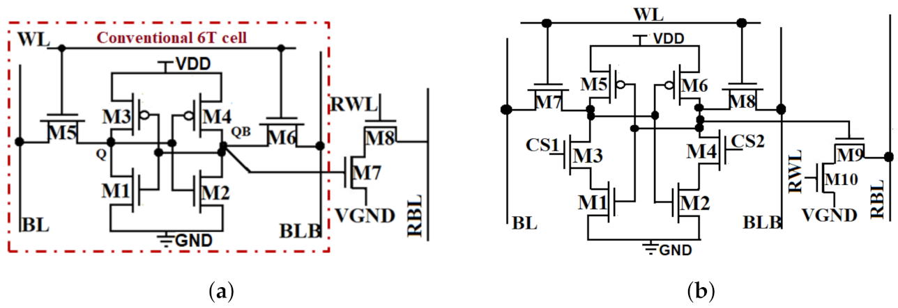
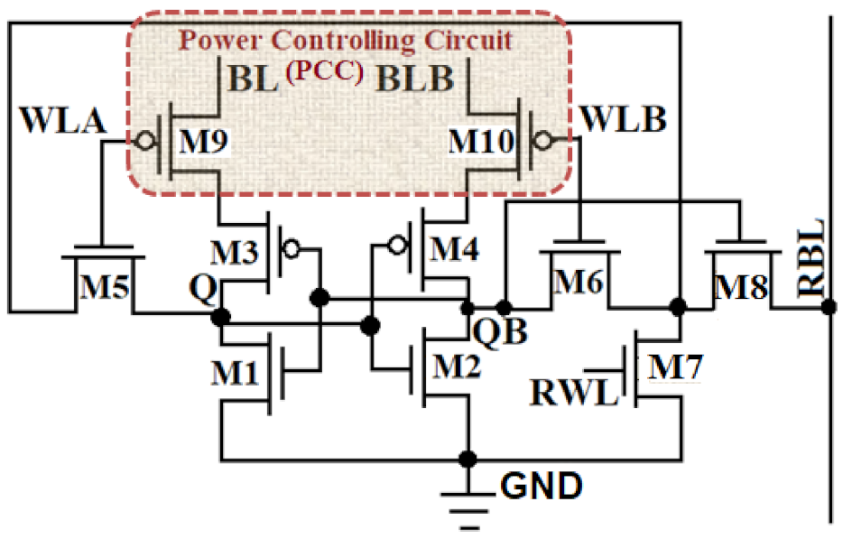
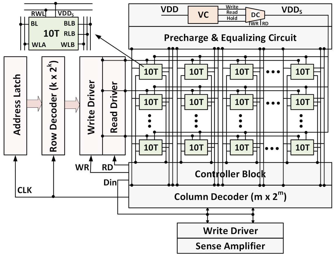
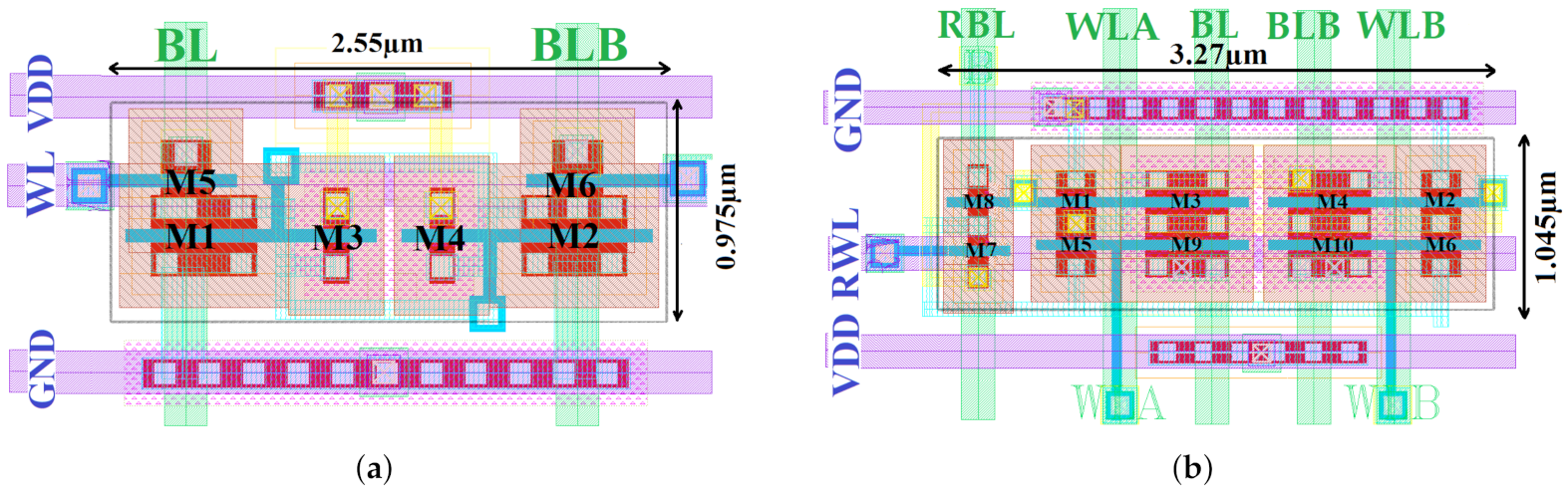
2. Proposed D2LP10T SRAM Cell Design
- The power controlling circuit (PCC) isolates the circuit from the power supply and inherently reduces the write power of the cell.
- The isolated read path is used to separate the read and write operation, which is resolved the read/write trade-off and enhanced the read stability.
- The write stability is enhanced with the support of a pull up inverter pair, and leakage power is reduced due to stacking combination design.
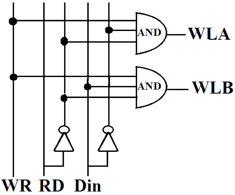
- The half-select issue is resolved by enabling the bit-line select signal, which is powered by the power controlling circuit.
3. Proposed Reconfigurable VDD (R-VDD) Scaled Memory Architecture
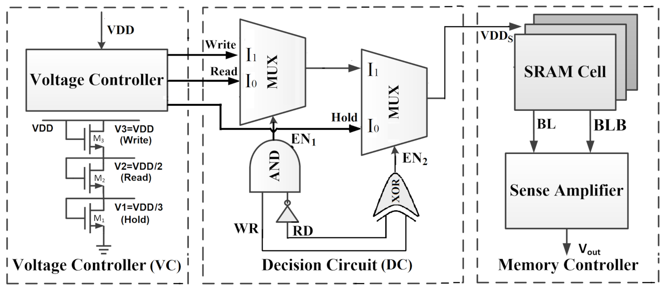
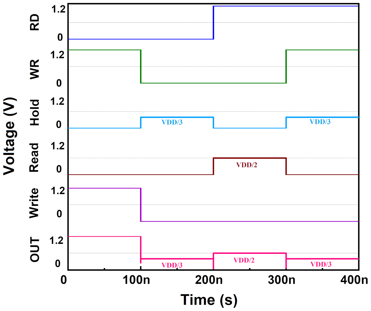
3.1. R-VDD Scaled Circuit (Voltage Controller and Decision Circuit)
| Algorithm 1 Voltage controller (VC) and decision circuit (DC) operation in SRAM cells | |
| if Operation = Write then | |
| WR ← 1 | //Activate write signal |
| RD ← 0 | //Deactivate read signal |
| EN1 ← 1 and EN2 ← 1 | //Select MUX1 and MUX2 |
| VDDS ← VDD | |
| else | |
| if Operation = Read then | |
| WR ← 0 | //Disable write signal |
| RD ← 1 | //Enable read signal |
| EN1 ← 0 and EN2← 1 | //Select MUX1 and MUX2 |
| VDDS ← | |
| else | |
| if Operation = Hold then | |
| WR ← 0 or 1 | //Disable or enable write signal |
| RD ← 0 or 1 | //Enable or disable read signal |
| EN1 ← 0 and EN2 ← 0 | //Select MUX1 and MUX2 |
| VDDS ← | |
| end if | |
| end if | |
| end if | |
3.2. Controller Block
3.3. R-VDD Scaled Architecture
4. Mechanism of Failure in SRAM Cell
- Read Failure— Due to the cause of random fluctuations in the threshold voltage (Vt); if the strength of access transistor increases (reduction in Vt) and the strength of pull-down NMOS transistor is reduced (increase in Vt), the circuit leads to read failure. Conversely, when reducing the strength of pull-up PMOS transistors, the chance to flip the cell content increases, which causes read failure.
- Write Failure— When a pull-up PMOS transistor is stronger and the access transistor is weaker, it can significantly degrade the discharging process and thereby cause a write failure. However, the write time of the cell is increased due to random variations in the device strength, leading to the inability to write data into the memory.
- Hold Failure— In standby mode, the supply voltage reduction causes the chance to disturb the stored data. Then it can be said that the cell has failed in hold mode. Either the Vt of M1 reduces when M3 increases or Vt of M2 increases when M4 reduces, so that the possibility of data flipping in the hold mode increases as shown in Figure 2.
5. Simulation Results and Discussion
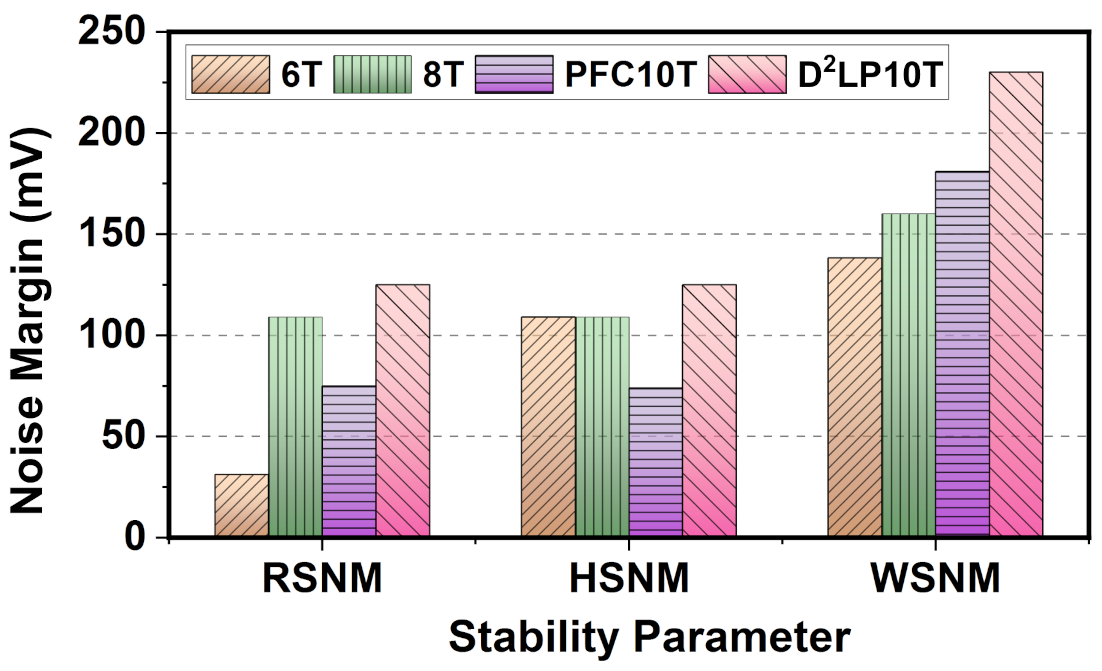
5.1. Stability Analysis
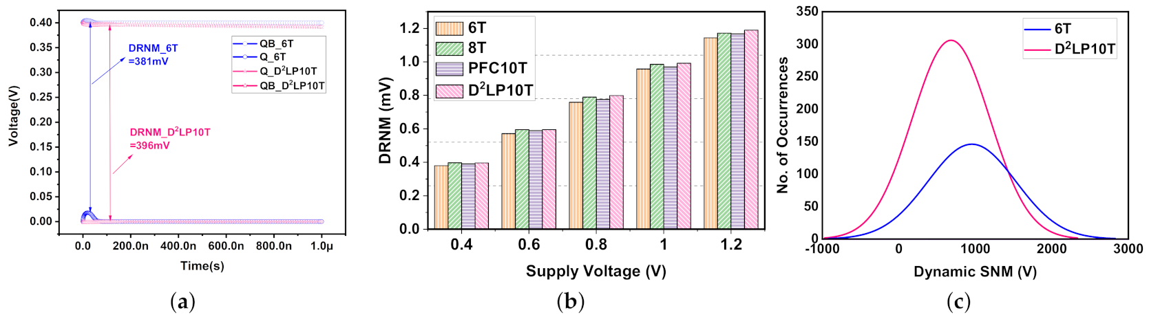
5.2. Dynamic Read Noise Margin
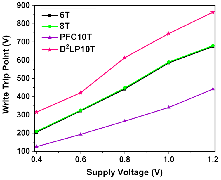
5.3. Write Trip Point
5.4. Failure Probability
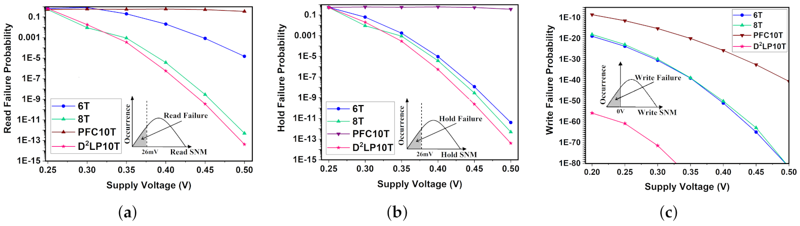
5.4.1. Read Failure Probability
5.4.2. Hold Failure Probability
5.4.3. Write Failure Probability
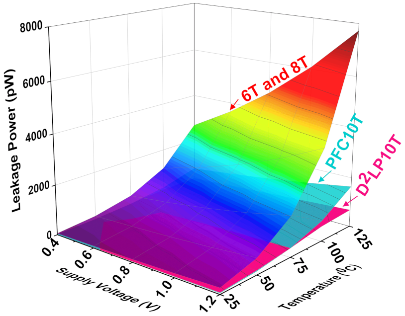
5.5. Leakage Power
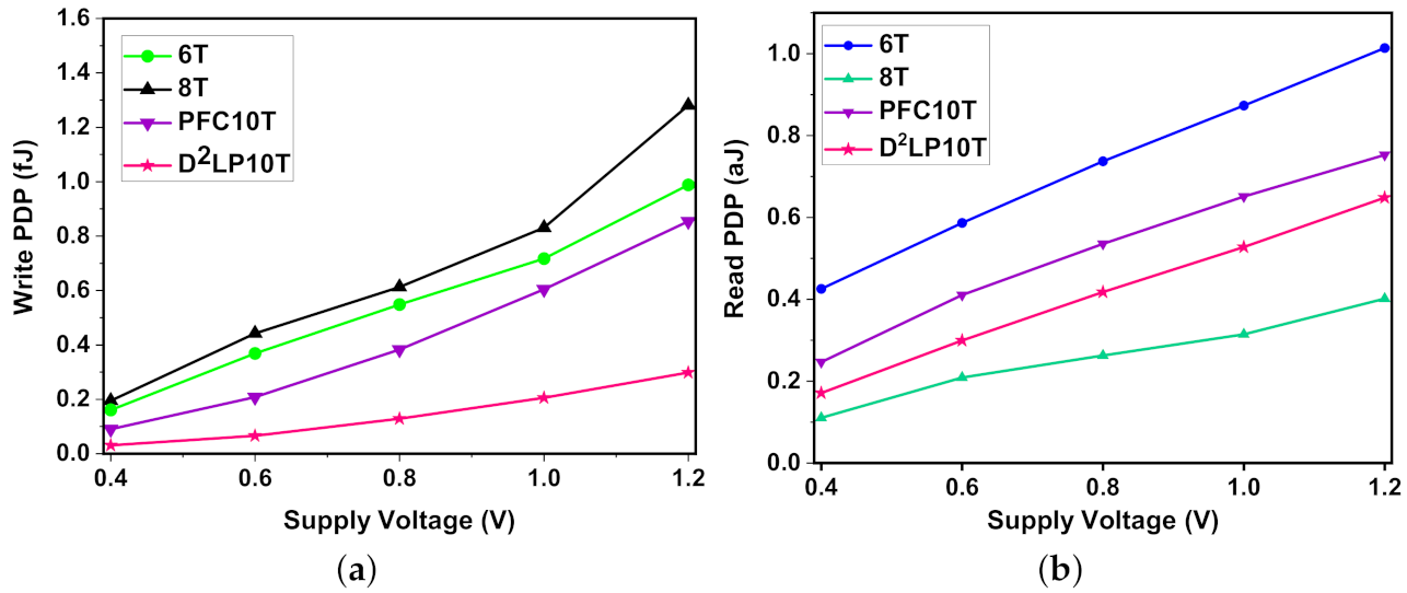
5.6. Write and Read PDP
5.7. Cell Area Comparison
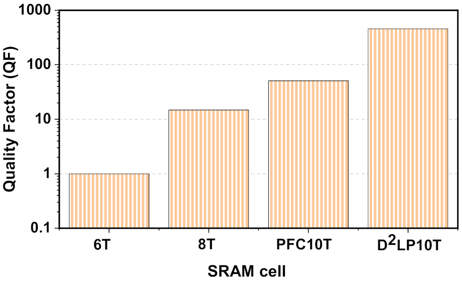
5.8. Quality Factor (QF)
5.9. Power Consumption in Memory Architecture
6. Conclusions
Author Contributions
Funding
Informed Consent Statement
Data Availability Statement
Acknowledgments
Conflicts of Interest
References
- Patrick, G.; Gattani, A. Memory Plays a Vital Role in Building the Connected World; Electronic Design: Hong Kong, China, 2015. [Google Scholar]
- Hodge, V.J.; O’Keefe, S.; Weeks, M.; Moulds, A. Wireless sensor networks for condition monitoring in the railway industry: A survey. IEEE Trans. Intell. Transp. Syst. 2014, 16, 1088–1106. [Google Scholar] [CrossRef]
- Leblebici, Y. CMOS Digital Integrated Circuits: Analysis and Design; McGraw-Hill College: New York, NY, USA, 1996. [Google Scholar]
- Sharma, V.; Bisht, P.; Dalal, A.; Gopal, M.; Vishvakarma, S.K.; Chouhan, S.S. Half-select free bit-line sharing 12T SRAM with double-adjacent bits soft error correction and a reconfigurable FPGA for low-power applications. AEU-Int. J. Electron. Commun. 2019, 104, 10–22. [Google Scholar] [CrossRef]
- Kim, T.H.; Jeong, H.; Park, J.; Kim, H.; Song, T.; Jung, S.O. An Embedded Level-Shifting Dual-Rail SRAM for High-Speed and Low-Power Cache. IEEE Access 2020, 8, 187126–187139. [Google Scholar] [CrossRef]
- Ling, M.; Shang, X.; Shen, S.; Shao, T.; Yang, J. Lowering the hit latencies of low voltage caches based on the cross-sensing timing speculation SRAM. IEEE Access 2019, 7, 111649–111661. [Google Scholar] [CrossRef]
- Ahmad, S.; Alam, N.; Hasan, M. Pseudo differential multi-cell upset immune robust SRAM cell for ultra-low power applications. AEU-Int. J. Electron. Commun. 2018, 83, 366–375. [Google Scholar] [CrossRef]
- Kang, S.M.; Leblebici, Y. CMOS Digital Integrated Circuits; Tata McGraw-Hill Education: New Delhi, India, 2003. [Google Scholar]
- Pal, S.; Bose, S.; Ki, W.H.; Islam, A. Characterization of half-select free write assist 9T SRAM cell. IEEE Trans. Electron Devices 2019, 66, 4745–4752. [Google Scholar] [CrossRef]
- Chang, I.J.; Kim, J.J.; Park, S.P.; Roy, K. A 32 kb 10T subthreshold SRAM array with bit-interleaving and differential read scheme in 90 nm CMOS. IEEE J. Solid-State Circuits 2008, 44, 388–622. [Google Scholar]
- Bharti, P.K.; Surana, N.; Mekie, J. Hetro8T: Power and area efficient approximate heterogeneous 8T SRAM for H. 264 video decoder. IET Comput. Digit. Tech. 2019, 13, 505–513. [Google Scholar] [CrossRef]
- Singh, P.; Reniwal, B.S.; Vijayvargiya, V.; Sharma, V.; Vishvakarma, S.K. Ultra low power-high stability, positive feedback controlled (PFC) 10T SRAM cell for look up table (LUT) design. Integration 2018, 62, 1–13. [Google Scholar] [CrossRef]
- Ahmad, S.; Gupta, M.K.; Alam, N.; Hasan, M. Single-ended Schmitt-trigger-based robust low-power SRAM cell. IEEE Trans. Very Large Scale Integr. (VLSI) Syst. 2016, 24, 2634–2642. [Google Scholar] [CrossRef]
- Lorenzo, R.; Pailly, R. Single bit-line 11T SRAM cell for low power and improved stability. IET Comput. Digit. Tech. 2020, 14, 114–121. [Google Scholar] [CrossRef]
- Chiu, Y.W.; Hu, Y.H.; Tu, M.H.; Zhao, J.K.; Chu, Y.H.; Jou, S.J.; Chuang, C.T. 40 nm bit-interleaving 12T subthreshold SRAM with data-aware write-assist. IEEE Trans. Circuits Syst. I Regul. Pap. 2014, 61, 2578–2585. [Google Scholar] [CrossRef]
- Gupta, N.; Sharma, V.; Shah, A.P.; Khan, S.; Huebner, M.; Vishvakarma, S.K. An Energy Efficient Data-Dependent Low-Power 10T SRAM Cell Design for LiFi Enabled Smart Street Lighting System Application. Int. J. Numer. Model. Electron. Netw. Devices Fields 2020, 33, e2766. [Google Scholar] [CrossRef]
- Gupta, N.; Shah, A.P.; Kumar, R.S.; Gupta, T.; Khan, S.; Vishvakarma, S.K. On-Chip Adaptive VDD Scaled Architecture of Reliable SRAM Cell with Improved Soft Error Tolerance. IEEE Trans. Device Mater. Reliab. 2020, 20, 694–705. [Google Scholar] [CrossRef]
- Kim, J.; Mazumder, P. A robust 12T SRAM cell with improved write margin for ultra-low power applications in 40 nm CMOS. Integr. VLSI J. 2017, 57, 1–10. [Google Scholar] [CrossRef] [Green Version]
- Chang, L.; Fried, D.M.; Hergenrother, J.; Sleight, J.W.; Dennard, R.H.; Montoye, R.K.; Sekaric, L.; McNab, S.J.; Topol, A.W.; Adams, C.D.; et al. Stable SRAM cell design for the 32 nm node and beyond. In Proceedings of the Digest of Technical Papers. 2005 Symposium on VLSI Technology, Kyoto, Japan, 14–16 June 2005; pp. 128–129. [Google Scholar]
- Bozzoli, L.; Sterpone, L. An Optimized Frame-Driven Routing Algorithm for Reconfigurable SRAM-Based FPGAs. IEEE Access 2020, 8, 116226–116238. [Google Scholar] [CrossRef]
- Shah, A.P.; Yadav, N.; Beohar, A.; Vishvakarma, S.K. On-chip adaptive body bias for reducing the impact of NBTI on 6T SRAM cells. IEEE Trans. Semicond. Manuf. 2018, 31, 242–249. [Google Scholar] [CrossRef]
- Kulkarni, J.P.; Roy, K. Ultralow-voltage process-variation-tolerant schmitt-trigger-based SRAM design. IEEE Trans. VLSI Syst. 2012, 20, 319–332. [Google Scholar] [CrossRef]
- Chang, M.H.; Chiu, Y.T.; Hwang, W. Design and Iso-Area Vmin Analysis of 9T Subthreshold SRAM With Bit-Interleaving Scheme in 65-nm CMOS. IEEE Trans. Circuits Syst. II Express Briefs 2012, 59, 429–433. [Google Scholar] [CrossRef] [Green Version]
- Mukhopadhyay, S.; Mahmoodi, H.; Roy, K. Modeling of failure probability and statistical design of SRAM array for yield enhancement in nanoscaled CMOS. IEEE Trans. Comput.-Aided Des. Integr. Circuits Syst. 2005, 24, 1859–1880. [Google Scholar] [CrossRef]
- Taub, H.; Schilling, D.L. Principles of Communication Systems; McGraw-Hill Higher Education: New Delhi, India, 1986. [Google Scholar]
- Proakis, J.G.; Salehi, M. Fundamentals of Communication Systems; Pearson Education India: Delhi, India, 2007. [Google Scholar]
- Ghosh, S.; Roy, K. Parameter variation tolerance and error resiliency: New design paradigm for the nanoscale era. Proc. IEEE 2010, 98, 1718–1751. [Google Scholar] [CrossRef]
- Ahmad, S.; Gupta, M.K.; Alam, N.; Hasan, M. Low leakage single bitline 9T (SB9T) static random access memory. Microelectron. J. 2017, 62, 1–11. [Google Scholar] [CrossRef]
- Seevinck, E.; List, F.J.; Lohstroh, J. Static-noise margin analysis of MOS SRAM cells. IEEE J. Solid-State Circuits 1987, 22, 748–754. [Google Scholar] [CrossRef] [Green Version]
- Sharma, V.; Gopal, M.; Singh, P.; Vishvakarma, S.K. A 220 mV robust read-decoupled partial feedback cutting based low-leakage 9T SRAM for Internet of Things (IoT) applications. AEU-Int. J. Electron. Commun. 2018, 87, 144–157. [Google Scholar] [CrossRef]


| Control Signals | Operation | |||
|---|---|---|---|---|
| Write 0 | Write 1 | Read | Hold | |
| WLA | 1 | 0 | 0 | 0 |
| WLB | 0 | 1 | 0 | 0 |
| RWL | 1 | 1 | 1 | 0 |
| BL | 0 | 1 | 1 (floating) | 1 (floating) |
| BLB | 1 | 0 | 1 (floating) | 1 (floating) |
| Supply Voltage (V) | Conventional Architecture | R-VDD Scaled Architecture | Reduction (in %) |
|---|---|---|---|
| 0.4 | 1.183 | 0.638 | 46.07 |
| 0.6 | 40.14 | 22.87 | 43.02 |
| 0.8 | 279 | 164 | 41.22 |
| 1.0 | 936.4 | 559 | 40.3 |
| 1.2 | 2343 | 1410 | 39.82 |
| Supply Voltage (V) | Conventional Architecture | R-VDD Scaled Architecture | Reduction (in %) |
|---|---|---|---|
| 0.4 | 0.275 | 0.071 | 74.55 |
| 0.6 | 1.917 | 0.521 | 72.82 |
| 0.8 | 12.24 | 3.47 | 71.65 |
| 1.0 | 48.74 | 15.57 | 68.05 |
| 1.2 | 147.84 | 54.51 | 63.13 |
Publisher’s Note: MDPI stays neutral with regard to jurisdictional claims in published maps and institutional affiliations. |
© 2021 by the authors. Licensee MDPI, Basel, Switzerland. This article is an open access article distributed under the terms and conditions of the Creative Commons Attribution (CC BY) license (https://creativecommons.org/licenses/by/4.0/).
Share and Cite
Gupta, N.; Shah, A.P.; Khan, S.; Vishvakarma, S.K.; Waltl, M.; Girard, P. Error-Tolerant Reconfigurable VDD 10T SRAM Architecture for IoT Applications. Electronics 2021, 10, 1718. https://doi.org/10.3390/electronics10141718
Gupta N, Shah AP, Khan S, Vishvakarma SK, Waltl M, Girard P. Error-Tolerant Reconfigurable VDD 10T SRAM Architecture for IoT Applications. Electronics. 2021; 10(14):1718. https://doi.org/10.3390/electronics10141718
Chicago/Turabian StyleGupta, Neha, Ambika Prasad Shah, Sajid Khan, Santosh Kumar Vishvakarma, Michael Waltl, and Patrick Girard. 2021. "Error-Tolerant Reconfigurable VDD 10T SRAM Architecture for IoT Applications" Electronics 10, no. 14: 1718. https://doi.org/10.3390/electronics10141718
APA StyleGupta, N., Shah, A. P., Khan, S., Vishvakarma, S. K., Waltl, M., & Girard, P. (2021). Error-Tolerant Reconfigurable VDD 10T SRAM Architecture for IoT Applications. Electronics, 10(14), 1718. https://doi.org/10.3390/electronics10141718