
A New Converter for Non-Isolated PV Systems

Abstract
:1. Introduction
2. Proposed Converter
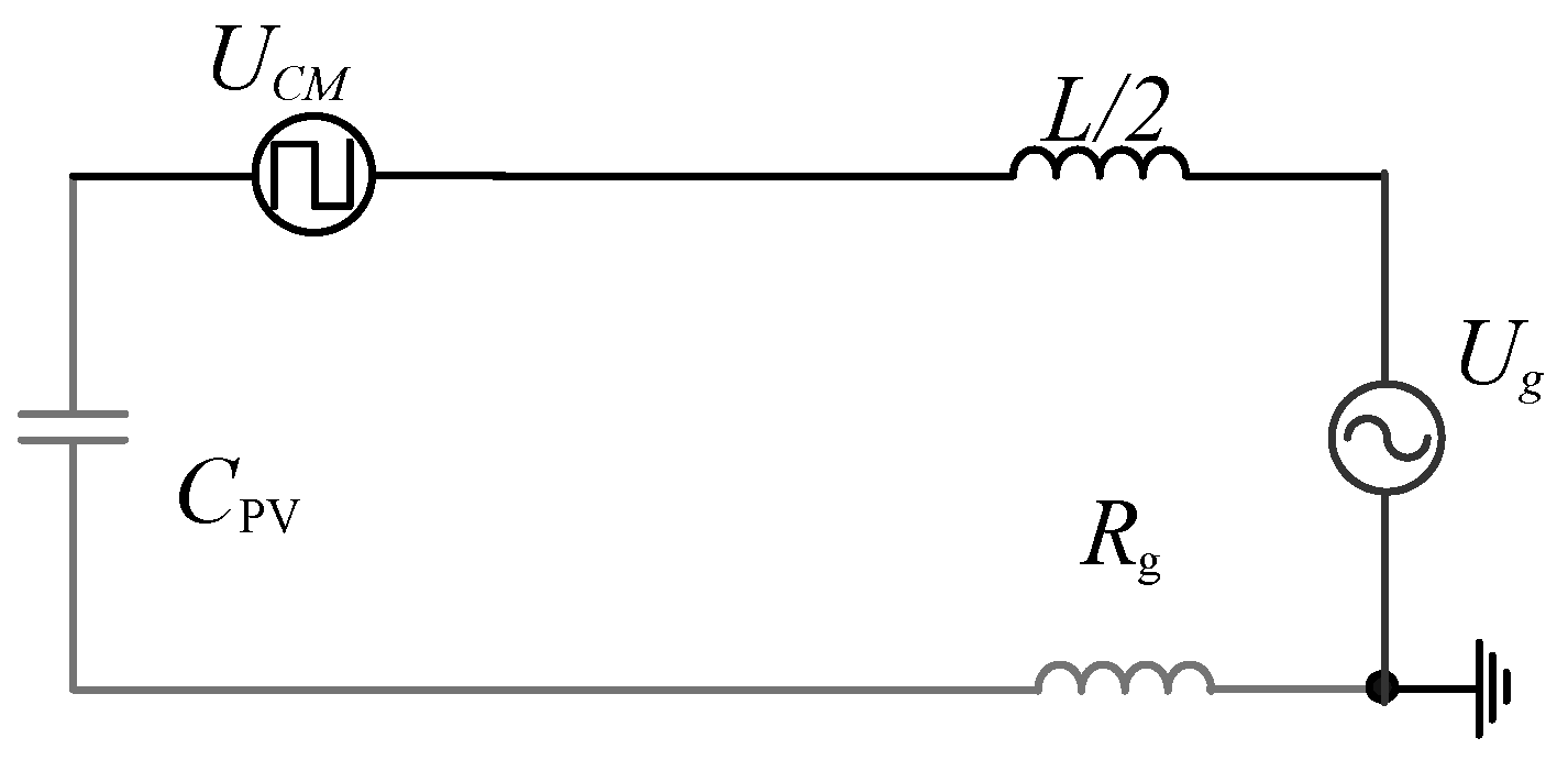
2.1. Circuit Configuration
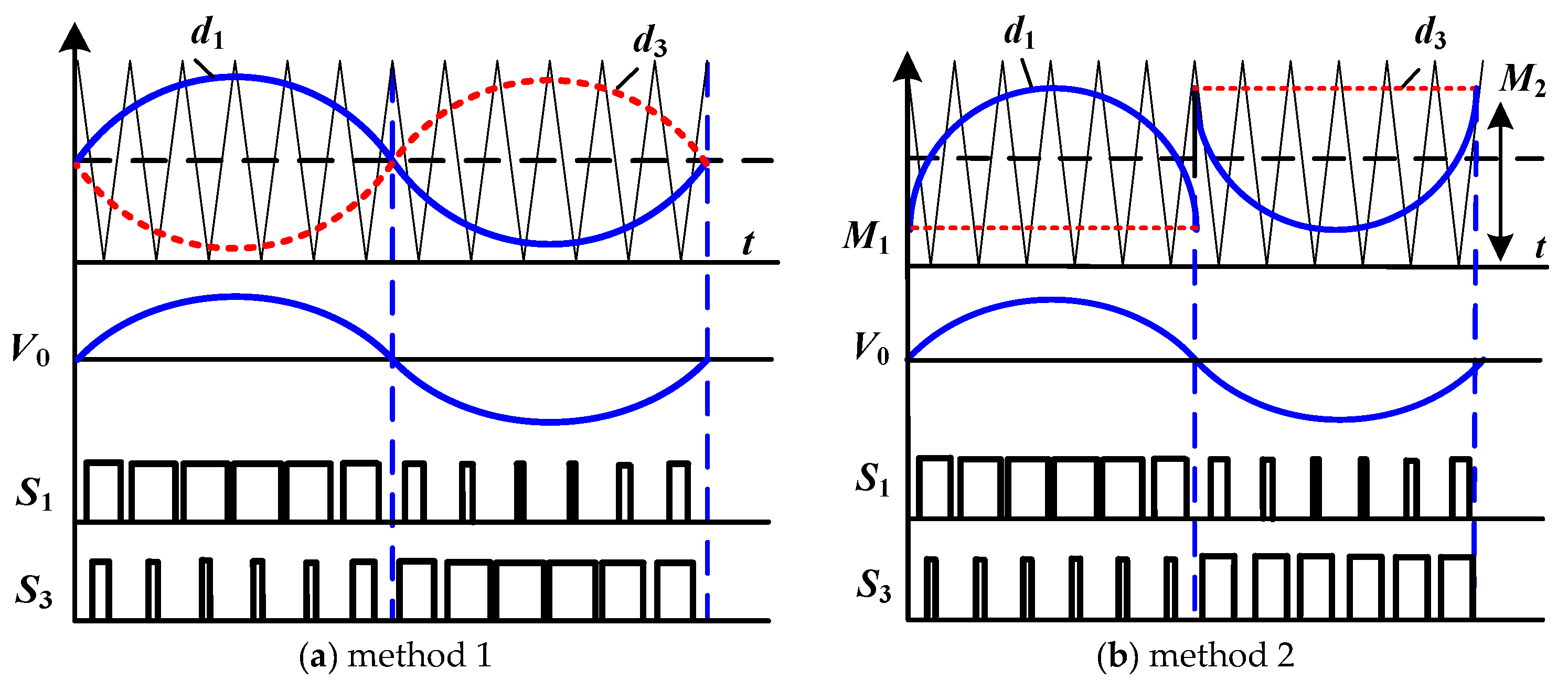
2.2. Modulation
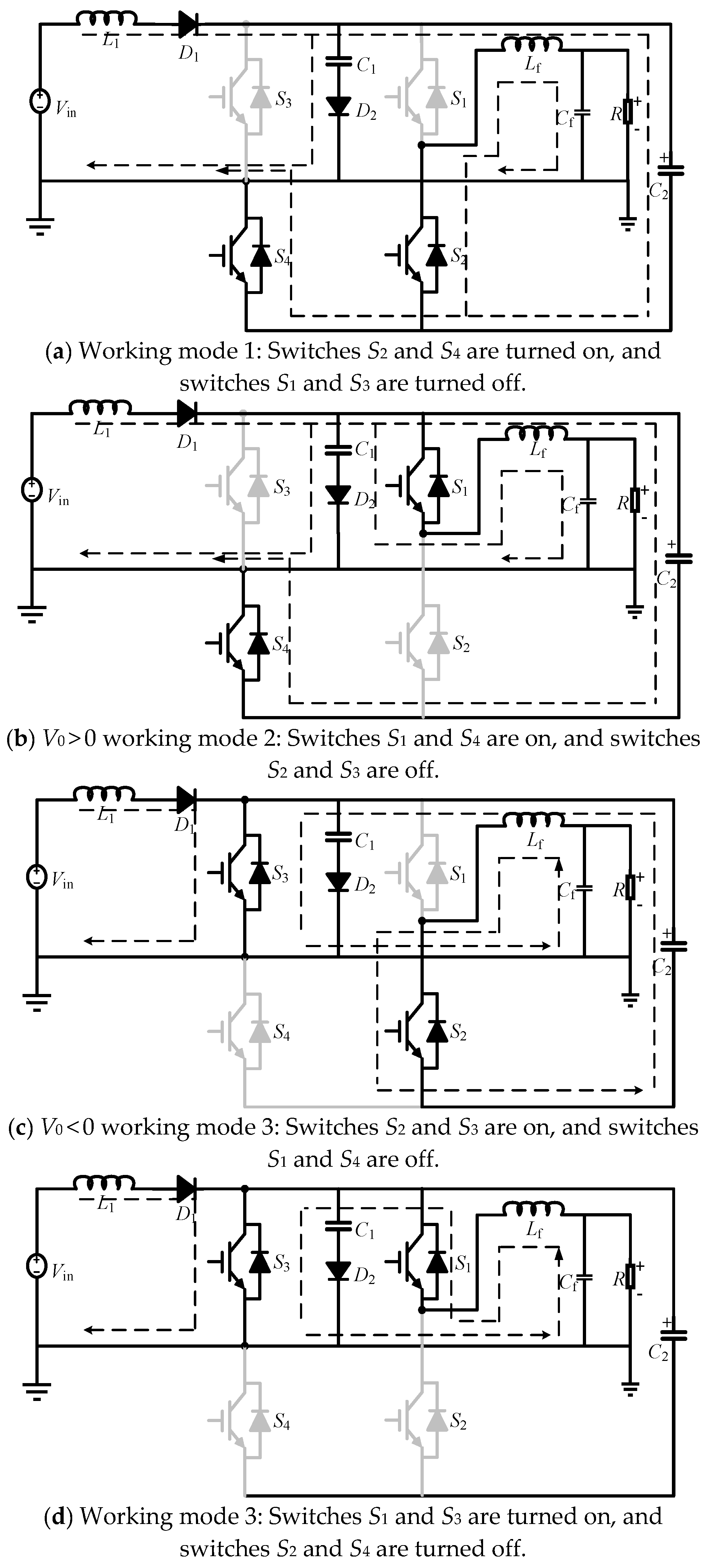
2.3. Operating Mode
2.4. Parameter Design
2.5. Comparative Study
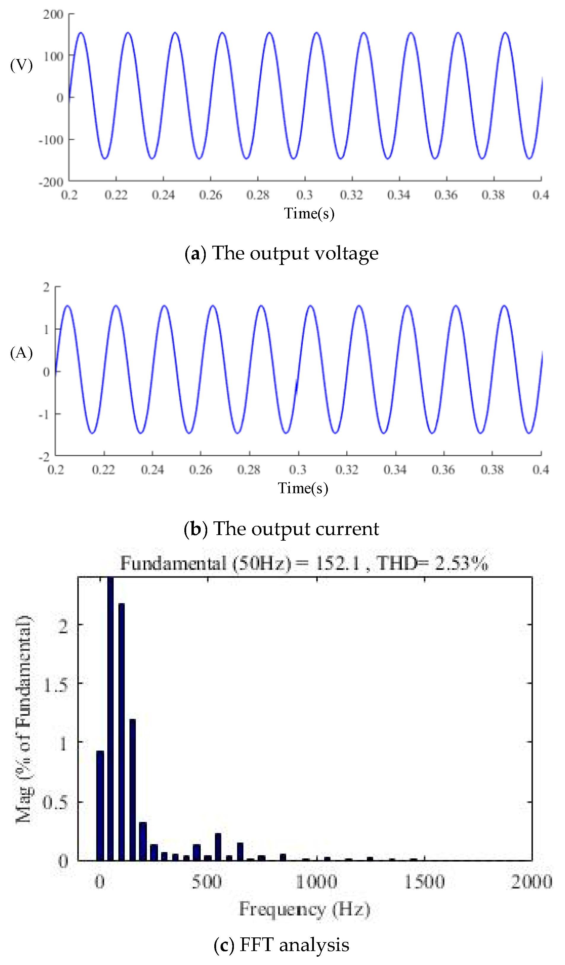
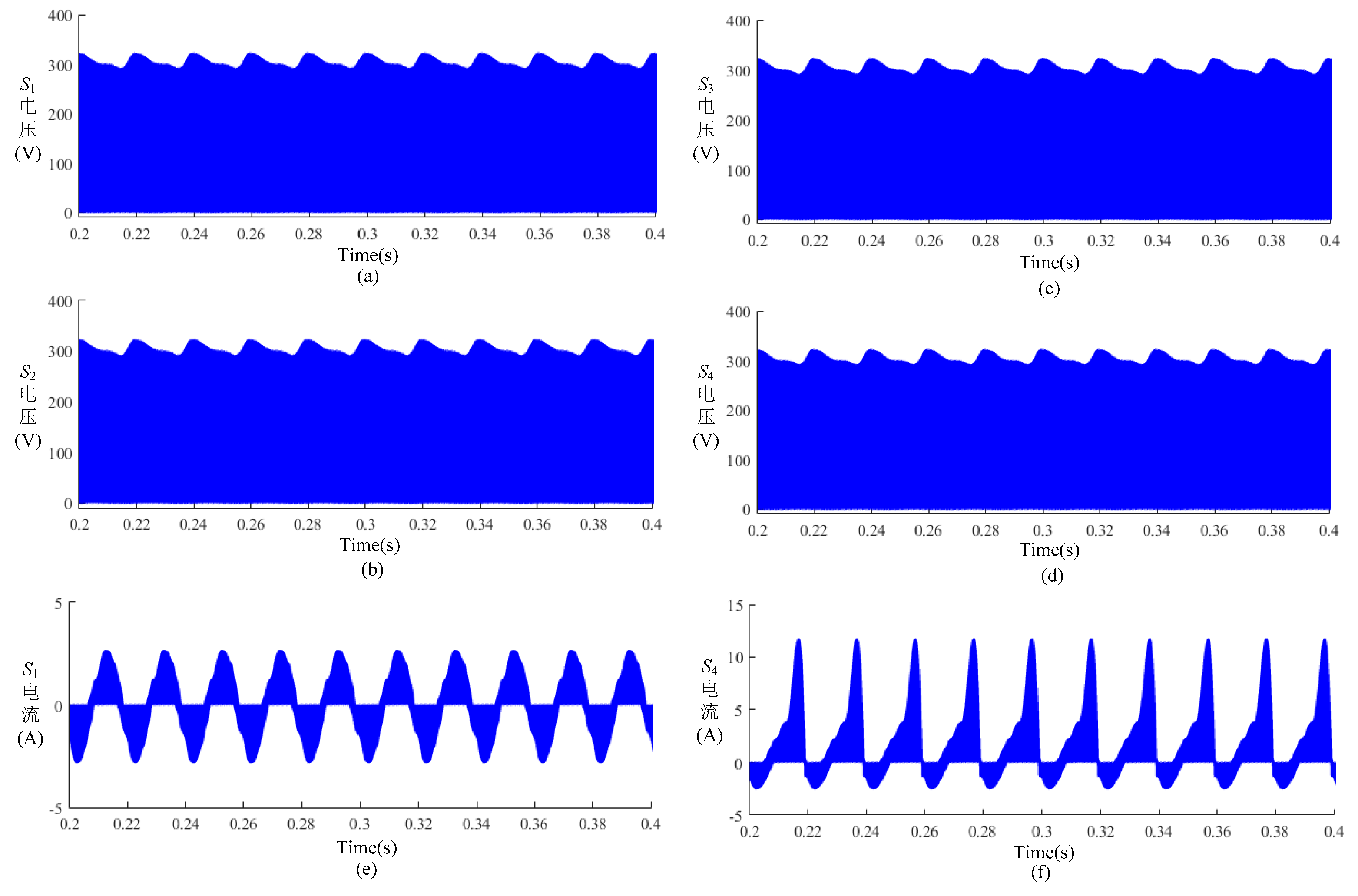
3. Simulation Results
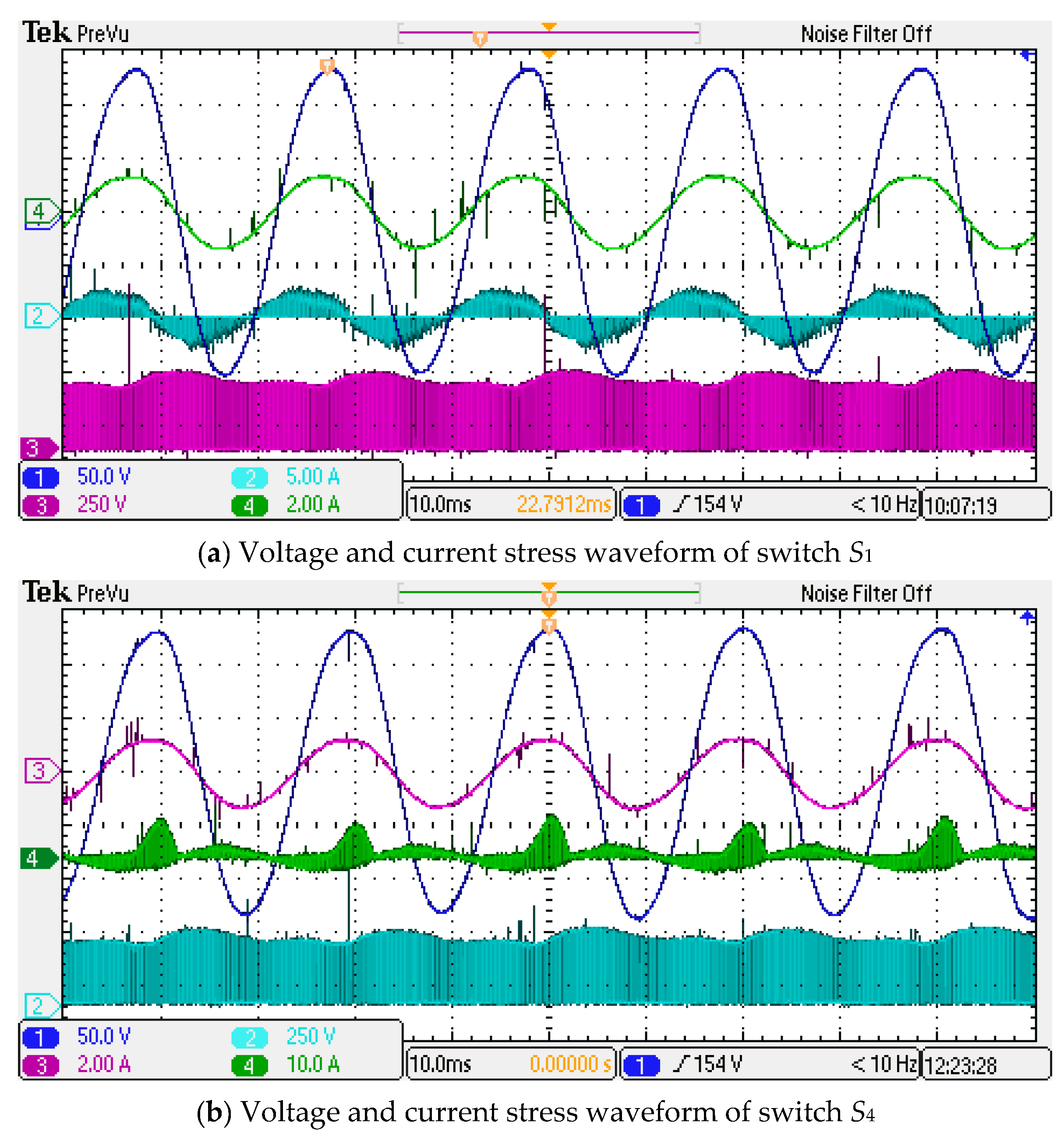
4. Experimental Results
5. Conclusions
Author Contributions
Funding
Conflicts of Interest
References
- Nguyen, M.-K. Power Converters in Power Electronics: Current Research Trends. Electronics 2020, 9, 654. [Google Scholar] [CrossRef]
- Fathabadi, H. Improving the Power Efficiency of a PV Power Generation System Using a Proposed Electrochemical Heat Engine Embedded in the System. IEEE Trans. Power Electron. 2019, 34, 8626–8633. [Google Scholar] [CrossRef]
- Jain, S.; Sonti, V. A highly efficient and reliable inverter configuration based cascaded multilevel inverter for PV systems. IEEE Trans. Ind. Electron. 2017, 64, 2865–2875. [Google Scholar] [CrossRef]
- Ji, Y.; Yang, Y.; Zhou, J.; Ding, H.; Guo, X.; Padmanaban, S. Control Strategies of Mitigating Dead-time Effect on Power Converters: An Overview. Electronics 2019, 8, 196. [Google Scholar] [CrossRef] [Green Version]
- Li, X.; Wang, N.; San, G.; Guo, X. Current Source AC-Side Clamped Inverter for Leakage Current Reduction in Grid-Connected PV System. Electronics 2019, 8, 129. [Google Scholar] [CrossRef] [Green Version]
- Breazeale, L.C.; Ayyanar, R. A photovoltaic array transformer-less inverter with film capacitors and silicon carbide transistors. IEEE Trans. Power Electron. 2015, 30, 1297–1305. [Google Scholar] [CrossRef]
- Tang, Y.; Yao, W.; Loh, P.C.; Blaabjerg, F. Highly reliable transformerless photovoltaic inverters with leakage current and pulsating power elimination. IEEE Trans. Ind. Electron. 2016, 63, 1016–1026. [Google Scholar] [CrossRef]
- Moorthy, R.S.K.; Rathore, A.K. Soft switching non-isolated current-fed inverter for PV/Fuel-cell applications. In Proceedings of the IEEE International Conference on Power Electron, Mumbai, India, 16–19 December 2014; pp. 1–6. [Google Scholar]
- Xue, Y.; Chang, L.; Kjaer, S.B.; Bordonau, J.; Shimizu, T. Topologies of single-phase inverters for small distributed power generators: An overview. IEEE Trans. Power Electron. 2004, 19, 1305–1314. [Google Scholar] [CrossRef]
- Koutroulis, E.; Kalaitzakis, K.; Voulgaris, N.C. Development of a microcontroller-based, photovoltaic maximum power point tracking control system. IEEE Trans. Power Electron. 2001, 16, 46–54. [Google Scholar] [CrossRef] [Green Version]
- Zhang, J.; Ding, H.; Wang, B.; Guo, X.; Padmanaban, S. Active Power Decoupling for Current Source Converters: An Overview Scenario. Electronics 2019, 8, 197. [Google Scholar] [CrossRef] [Green Version]
- Guo, X.; Yang, Y.; Zhu, T. ESI: A novel three-phase inverter with leakage current attenuation for transformerless PV systems. IEEE Trans. Ind. Electron. 2018, 65, 2967–2974. [Google Scholar] [CrossRef]
- Anandababu, C.; Fernandes, B.G. Leakage current generation in view of circuit topology of non-isolated full-bridge neutral point clamped grid-tied photovoltaic inverters. IET Power Electron. 2016, 9, 1571–1580. [Google Scholar] [CrossRef]
- Xiao, G.; Yang, Y.; He, R.; Wang, B.; Blaabjerg, F. Transformerless Z-source four-leg PV inverter with leakage current reduction. IEEE Trans. Power Electron. 2019, 34, 4343–4352. [Google Scholar]
- Vázquez, N.; Vázquez, J.; Váquero, J.; Hernández, C.; Vázquez, E.; Osorio, R. Integrating two stages as a common-mode transformerless photovoltaic converter. IEEE Trans. Ind. Electron. 2017, 64, 7498–7507. [Google Scholar] [CrossRef]
- Kumar, A.; Sensarma, P. A four-switch single-stage single-phase buck–boost inverter. IEEE Trans. Power Electron. 2017, 32, 5282–5292. [Google Scholar] [CrossRef]
- Hu, X.; Ma, P.; Gao, B.; Zhang, M. An Integrated Step-Up Inverter without Transformer and Leakage Current for Grid-Connected Photovoltaic System. IEEE Trans. Power Electron. 2019, 34, 9814–9827. [Google Scholar] [CrossRef]
- Mahmoudian, M.; Rodrigues, E.M.G.; Pouresmaeil, E. An Efficient H7 Single-Phase Photovoltaic Grid Connected Inverter for CMC Conceptualization and Mitigation Method. Electronics 2020, 9, 1440. [Google Scholar] [CrossRef]
- Guo, X.; Wang, N.; Wang, B.; Lu, Z.; Blaabjerg, F. Evaluation of three-phase transformerless dc-bypass PV inverters for leakage current reduction. IEEE Trans. Power Electron. 2020, 35, 5918–5927. [Google Scholar] [CrossRef]
- Xiao, G.; Jia, Y. Hardware-based cascaded topology and modulation strategy with leakage current reduction for transformerless PV systems. IEEE Trans. Ind. Electron. 2016, 62, 7823–7832. [Google Scholar]


| Topology | Switch | Step-Up Capability | Leakage Current |
|---|---|---|---|
| H4 + boost converter converter | 5 | Yes | High |
| H5 converter | 5 | No | Small |
| H6 converter | 6 | No | Small |
| oH5 converter | 6 | No | Very Small |
| Proposed converter | 4 | Yes | Zero |
| Parameter | Values |
|---|---|
| Input voltage Vin | 70 V |
| output voltage RMS | 110 V/50 Hz |
| Input inductance L1 | 5 mH |
| Capacitance C1 | 30 μF |
| Capacitance C2 | 50 μF |
| Capacitance Cf | 20 μF |
| Inductance Lf | 2 mH |
Publisher’s Note: MDPI stays neutral with regard to jurisdictional claims in published maps and institutional affiliations. |
© 2021 by the authors. Licensee MDPI, Basel, Switzerland. This article is an open access article distributed under the terms and conditions of the Creative Commons Attribution (CC BY) license (https://creativecommons.org/licenses/by/4.0/).
Share and Cite
Wang, H.; Lu, Z. A New Converter for Non-Isolated PV Systems. Electronics 2021, 10, 1716. https://doi.org/10.3390/electronics10141716
Wang H, Lu Z. A New Converter for Non-Isolated PV Systems. Electronics. 2021; 10(14):1716. https://doi.org/10.3390/electronics10141716
Chicago/Turabian StyleWang, Huaibao, and Zhigang Lu. 2021. "A New Converter for Non-Isolated PV Systems" Electronics 10, no. 14: 1716. https://doi.org/10.3390/electronics10141716
APA StyleWang, H., & Lu, Z. (2021). A New Converter for Non-Isolated PV Systems. Electronics, 10(14), 1716. https://doi.org/10.3390/electronics10141716