1. Introduction
Sunrise 3 is the third missions where a telescope will be launched into the stratosphere on a balloon from the Arctic Circle, and reaching an altitude of about forty kilometers, which avoids the day and night cycles and the image degradation caused by the terrestrial atmosphere. On this basis, it observes the Sun continuously for a few days [
1]. The IMaX/Sunrise project was originally approved in 2002 by the National Program as a strategic step towards a technological demonstrator for the Solar Orbiter magnetograph (PHI, Polarimetric and Helioseismic Imager) [
2]. The IMax (Imaging Magnetograph eXperiment) was one of the post-focus instruments of the one-meter solar telescope aboard the first Sunrise mission in 2009 [
3]. This mission studied the solar magnetism in a period of minimum solar activity [
4,
5].
The first Sunrise mission obtained excellent results and led to a second mission that took place in 2013 in a period of maximum solar activity [
6]. The success of the previous mission in 2009 meant that the design of the 2013 mission was largely unchanged. The gondola and the telescope were the same; the IMaX on the 2013 flight was also very similar to the version flown on Sunrise I, although a number of smaller changes and updates had been made. The parts replaced included the Field Programmable Gate Array (FPGA) in the proximity electronics and other components (filter system, retarders and so on). Most of these parts were replaced by nearly identical ones. Only the filter system of one of the instruments on board was modified [
7]. The scientific results of the Sunrise missions can be consulted at [
6,
7]. This second science flight allowed this balloon-borne solar observatory to obtain the first seeing-free observations of an active region close to the diffraction limit of the 1 m diameter telescope. These data are rich in information about a variety of solar phenomena at very high spatial resolution and at wavelengths that partly cannot be accessed from the ground [
7,
8,
9,
10,
11].
Rather than being a transient thought for a given phase of solar activity, Sunrise 3 is meant to observe the evolution of the magnetically coupled solar atmosphere at high spatial resolution. A new Tunable Magnetograph (TuMag) has been implemented for this mission. The TuMag instrument is a new, and improved, version of the IMaX instrument [
12]. Besides changing the cameras that were not very efficient and refurbish most of the optics and opto-mechanics accordingly, a major conceptual change in the optics has been realized due to the tunable capability of the instrument filter. TuMag provides 50 × 50 arcmin
2 images of the Sun in various narrow bands (~8 pm wide). From these images, the information of the four polarization states can be extracted [
13,
14,
15].
The electronic unit of TuMag instrument has been completely redesigned respect of the old IMaX. On the one hand, most of the former components were damaged after the second flight. On the other hand, the big old unit is inefficiently old-fashioned. New technologies have been easy to incorporate into a much smaller box. Therefore, current technological components have been used that will result in a much smaller system, leaving more physical space for the other instruments on board.
In relation to the TuMag camera sensor, hardware has been developed that includes two Printed Circuit Boards (PCB). The first of them contains a Complementary Metal-Oxide Semiconductor (CMOS) image sensor, the GPIXEL GSENSE400-BSI [
15]. The second one includes an Artix-7 XC7A50T-2CSG325C FPGA that is responsible for controlling the sensor and communicating with the Data Processing Unit (DPU) of the instrument through a CoaxPress interface [
16,
17]. Artix-7 FPGA device consists of an array of Configurable Logic Blocks (CLBs) which are composed of two slices. These elements are connected to other similar blocks via programmable interconnects and switch matrices. Inside of a slice there are four Lookup Tables (6-LUT) capable of implementing a logic function up to six inputs, a small memory (named distributed-memory) or a shift register. The Artix-7 XC7A50T-2CSG325C FPGA has 32,600 6-LUT and 16,300 slice registers. The FPGA implementation makes the designed algorithm, flexible, customizable, reconfigurable or reprogrammable with advantages of well-customized, integration, accessibility and expandability. The system can be resized according to its needs taking advantages of the VHDL configurability.
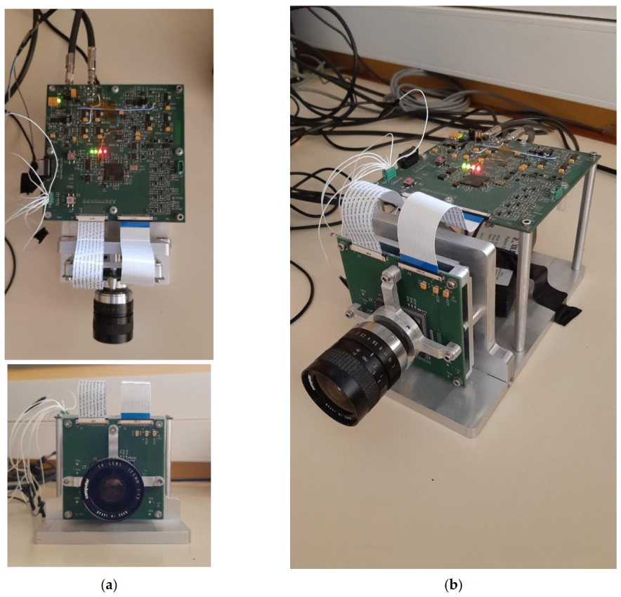
Figure 1 shows pictures of the first implemented prototype of the TuMag camera. The sensor PCB is located vertically and the FPGA PCB is located horizontally.
The GSENSE400 is a 4-megapixel (2048 × 2048) resolution CMOS image sensor with 11 μm photodiode pixels and it has been chosen to incorporate it into the detection system as it has a set of characteristics that meet the requirements of the scientific commissions of the Sunrise 3 mission, such as extremely low reading noise, high sensitivity, and high dynamic range features [
16].
The sensor has a 12-bit AD converter, a temperature sensor, a PLL and an SPI interface for control tasks. In order to configure the detector and start it up properly, we have to write to memory banks of the detector through this SPI interface.
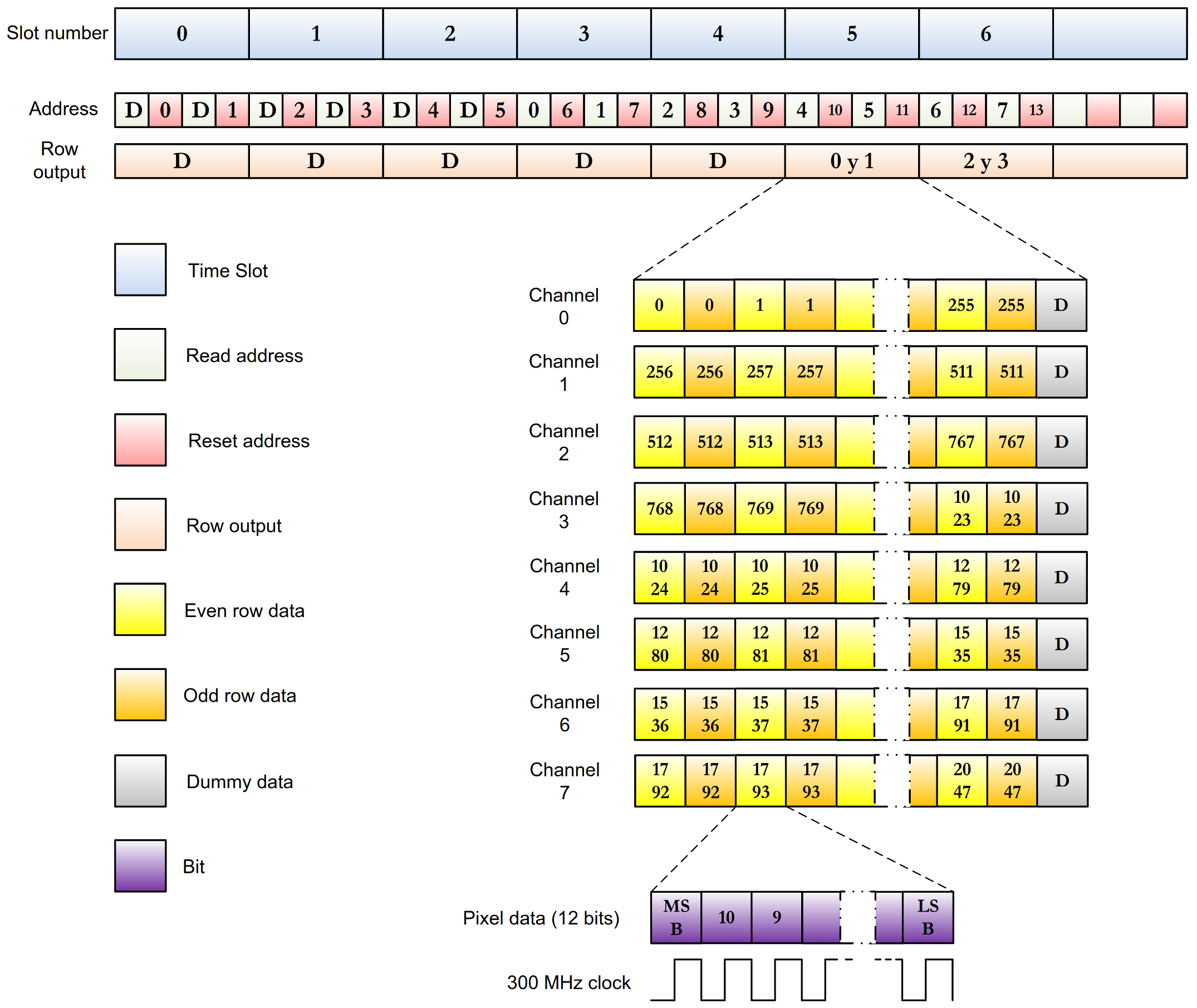
The sensor has eight differential channels, which provide 12-bit pixel data at 300 MHz, in order to send the image to the FPGA in serial format. The rows of the CMOS sensor are read or reset in time slots of 513-pixel clock cycles (25 MHz) using control signals that the Artix-7 FPGA must send to the sensor. These channels have to be calibrated so that the data can be correctly read. This task is performed by the FPGA [
18].
In addition, the format of the reading data is different of the row-by-column format, so an image ordering must be implemented in the FPGA firmware. This task has to be done in the FPGA that controls the sensor as the DPU has a high workload with the control of all the instruments, the telescope, the refrigeration, the navigation, communications and so on. Furthermore, the acquisition of the images must be carried out in very precise moments of time using a hardware trigger. For this reason, the time delays that any operating system or software program can cause should be avoided. The GPIXEL sensor supplies image data in eight-channel format. Therefore, we have implemented in firmware the image ordering. Due to the eight-channel format, the sensor only allows the acquired images to be cropped in height (rows), and not in width (columns). Therefore, the Region of Interest (RoI) that can be configured into the sensor is limited. The implemented VHDL module to order the image considers this limitation, and cuts the received data into columns as well, so that only the RoI is sent to the DPU. This prevents the CoaXPress communication channel from being overloaded with unnecessary data.
This work describes the FPGA implementation of Image Ordering and Packing algorithm for TuMag Camera concerning the real-time ordering of the images before grabbing and sending to the DPU. FPGA devices have proven to be ideal for implementing real-time algorithms for images coming from cameras for astrophysical applications [
19,
20,
21,
22,
23,
24,
25,
26]. In this case, the improved VHDL module allows cropping of the image in rows and columns, and is included in the driver that controls the TuMag camera. The TuMag instrument is part of the Sunrise 3 mission. The flight is scheduled for the northern summer of 2022.
The rest of the present work is organized as follows: The second section briefly describes the image sensor configuration, communication and operation. The third section details the firmware implemented in the FPGA with an emphasis on image ordering detailed in the fourth section. Then, in section five, we present the results and conclusions. Finally, the future work is presented.
2. Main Features of the Image Sensor
The GSENSE400 sensor is a 4-megapixel (2048 × 2048) resolution CMOS image sensor with 11 μm photodiode pixels. The sensor has an extremely low reading noise [
16]. It has two operation modes: In STD mode, the sensor works at 48 frames per second and in HDR mode, the sensor is optimized for high dynamic range applications and it works at 24 frames per second. The high sensitivity, low read noise, and high dynamic range feature makes it perfect for a variety of scientific applications, such as the one at hand.
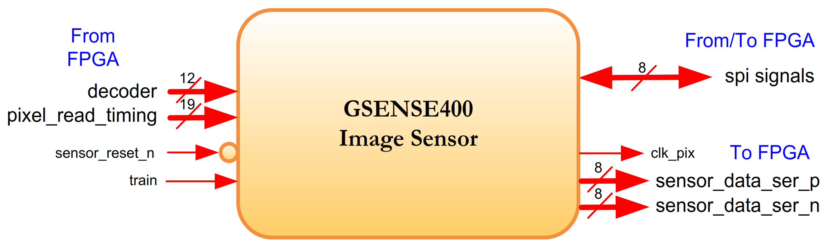
The sensor has a 12-bit AD converter, a temperature sensor, a PLL and an SPI interface for control tasks. The interface with the main ports of GSENSE400 sensor is depicted in
Figure 2. In order to configure the detector and start it up properly, we have to write to memory banks of the detector through an SPI interface (
spi signals). The sensor has eight differential channels that provide 12-bit pixel data at 300 MHz in order to send the image to the FPGA in serial format (
sensor_data_ser signals). The synchronism of these signals is supplied using a 25 MHz pixel clock (
clk_pix). User can calibrate these signals using a training word that is written in the register banks using the SPI interface. When
train signal is set to high, GSENSE400 sends the training word continuously through
sensor_data_ser signals. Finally, the firmware in FPGA supplies the timing control signals and the address of pixel rows directly to the sensor (
pixel_read_timing and
decoder). The values of these signals in time are described in [
16,
19].
The image sensor has two operation modes: In Standard (STD) mode, the sensor works at 48 frames per second and in high-dynamic range (HDR) mode, the sensor is optimized for high dynamic range applications and it works at 24 frames per second. In both modes, the rows of the CMOS sensor are read or reset in time slots of 513-pixel clock cycles (at 25 MHz) through control signals that the Artix-7 FPGA must send. In HDR mode, a time slot consists of 2 phases: One row read phase and one row reset phase. Using this mode, two readings are obtained for each direction, one in high gain and the other in low gain. This mode is not configured.
In STD mode, a time slot consists of 4 phases: Single row read phase, single row reset phase, and read and reset phases of subsequent rows, respectively.
Figure 3 shows how rows M and following are read and rows N and following are reset in two time slots [
16]. As mentioned previously, the implemented driver in FPGA sends decoder and
pixel_read_timing values for a right STD mode operation.
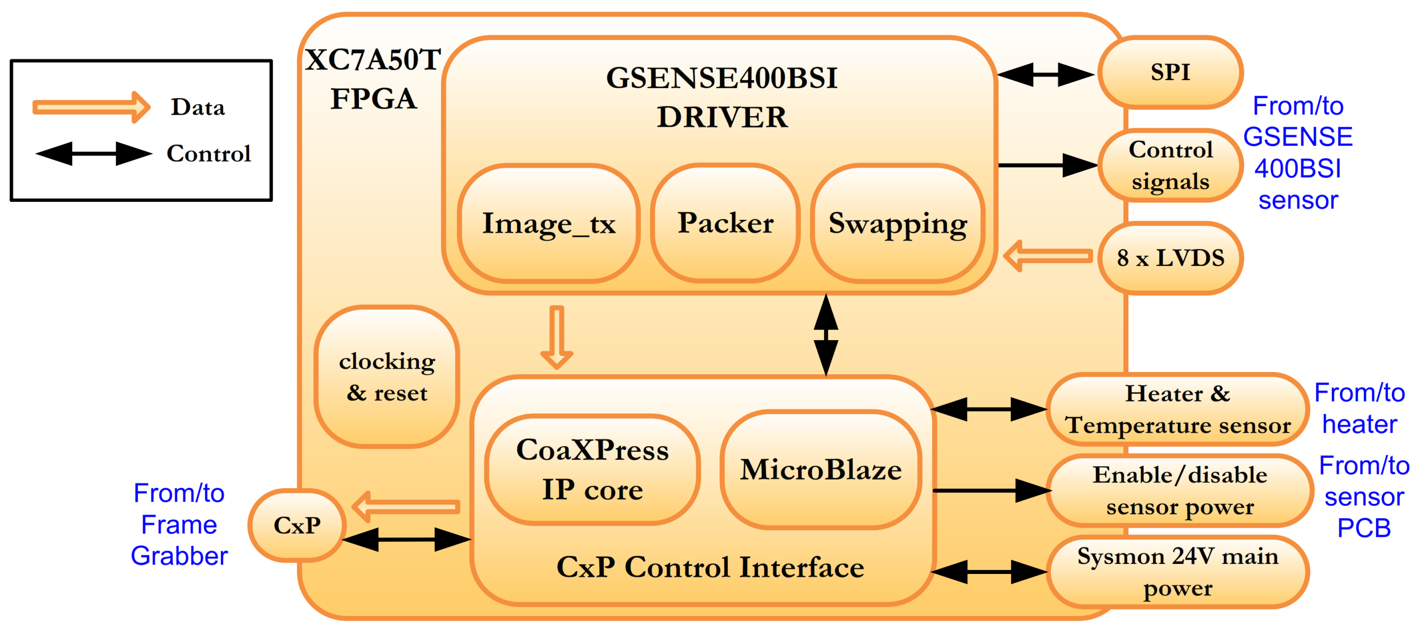
3. TuMag Camera Firmware Architecture
FPGA PBC contains the XC7A50T-2CSG325C Artix-7 FPGA that configures and communicates with the sensor. This one also features a CoaXPress interface for communication with the host/DPU system or with the Frame Grabber in the prototype [
18,
27,
28]. An overview of the camera FW architecture is depicted in
Figure 4.
Two main blocks can be distinguished, namely, GSENSE400-BSI driver and CoaXPress (CxP) Control Interface. The main function of CxP Control Interface module is the control of the CoaXPress device IP core, which implements the communication functionalities between the GSENSE400-BSI sensor and the Frame Grabber. The firmware implemented in the FPGA is in charge of controlling the image sensor, configuring it and grabbing images from it through a 3.125 Gbps CoaXPress interface [
18,
29,
30]. The camera is triggered through the same interface. For such a purpose, the architecture is based on an embedded Microblaze soft processor [
31]. This soft-core also manages a system monitor of the main power (24 V), a heater and controls the sensor on/off power.
The FPGA firmware allows the modification of several parameters as the Region of Interest (ROI), the exposure time, the number of frames to be acquired, the sensor gain and the black level offset to obtain the camera required functionality. The host sends these parameters to MicroBlaze through control signals of CxP interface and then MicroBlaze writes to a memory bank in the GSENSE driver. Finally, most of these parameters require writing to the sensor register bank. This is done through the SPI interface in
Figure 4.
Once the sensor is configured and calibrated, the driver waits for a read command. When this happens, the driver sends to the sensor the control signals and the read and reset rows (see
Figure 2) according to
Figure 3. Control signals are described in [
16]. The driver stores these values in a 513 × 19 memory and using a simple counter sends values correctly to the sensor. Decoder signal in
Figure 2 are calculated using row values of RoI (the beginning row and the size in rows, named
reg_window_row_start and
reg_window_row_length) and the exposure time (named
reg_integration).
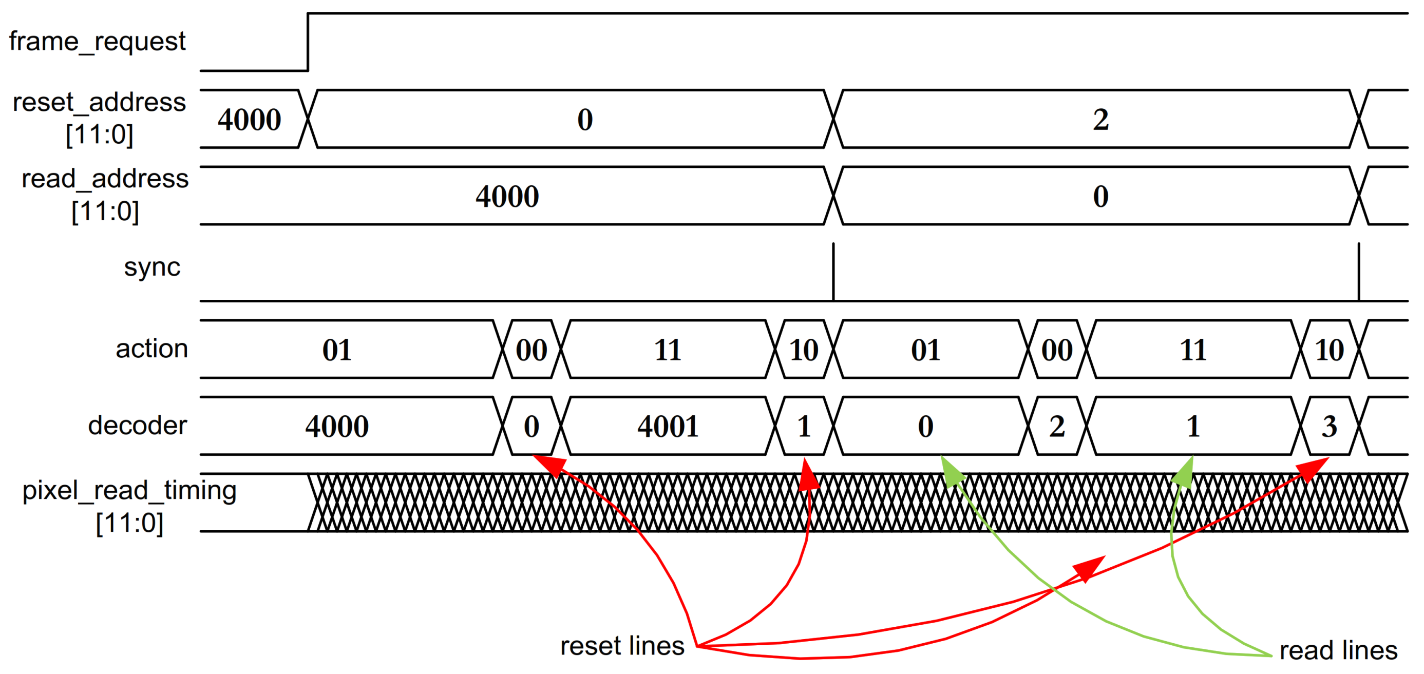
Figure 5 shows the signals that the driver sends to the sensor once it has been calibrated. When the driver receives a read image command (
frame_req set to high), it generates the reset and read addresses and the internal signal named
action, which decodes if a reset or a read is made of an odd or even row according
Table 1. The driver composes decoder signal with these internal values and send it with
pixel_read_timing signal through the corresponding image sensor ports (see
Figure 2). The values, 4000 and 4001 of the decoder are dummy addresses. Therefore, in the first time slot no read is realized and there are only rows reset operation. In the second time slot, the driver resets rows number 2 and 3 and reads rows number 0 and 1. The internal
sync signal (in red) specifies the end of a time slot and it is used to preserve synchronism with the data that the driver will receive from the sensor.
4. Image Ordering Algorithm
As mentioned in
Section 2, the rows of the CMOS sensor are read or reset in time slots of 513-pixel clock cycles (at 25 MHz) through control signals that the Artix-7 FPGA must send, according
Figure 3 in STD mode. This reset and read mode is performed simultaneously for the 8 channels, which distribute the 2048 rows of the sensor as is shown in
Table 2.
Figure 6 depicts the data output format in STD mode considering the time slots. For this example, the firmware resets rows from 0 to 13 in 7 time slots and reads consecutive rows starting from the time slot number 3. This number depends on the configured exposure time, which in this case is equivalent to 3 time slots. Before that time, the firmware sends dummy addresses (4000 and 4001 for even and odd rows). The sensor takes 2 time slots to send the data since the firmware sends the read address to the sensor. Then, and as can be seen in
Figure 6, every two rows simultaneously (even and odd), the sensor supplies the data as follows: channel 0, pixels from 0 to 255 of those two rows; channel 1, pixels 256 to 511, and so on. Therefore, the data must be sorted on two levels: by row parity and by channels.
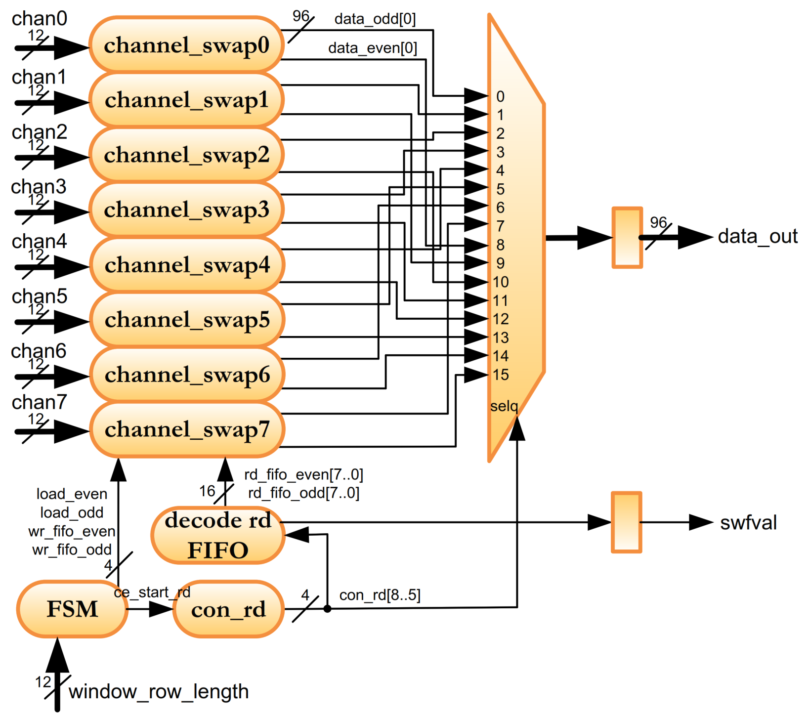
4.1. Swapping Module
In order to implement the ordering of the incoming image, a module named swapping has been designed (see
Figure 4). This module implements FIFOs (First-In First-Out components) and multiplexers in order to arrange the incoming 8-channel Low-voltage differential signalling (LVDS) data. There is two-level ordering: Parity arrange (odd and even rows) and channel arrange. It has been described using VHDL language and its interface is shown in
Figure 7. A brief description of each module port is also shown in
Table 3.
The detailed diagram of this module is shown in
Figure 8. For each channel, there is a channel swap submodule. Each submodule includes an even FIFO and an odd FIFO that are continuously swapping for classifying odd and even pixels. In order to implement the image ordering, the incoming data for each channel are stored into the FIFOs inside the
channel_swap submodules. An FSM that controls
con_rd counter, which in turn controls the read-out of
channel_swap and a 16-to-1 multiplexer, selects which data are sent to
data_out port. Each of the channel_swap submodules are made up of two 7-depth shift-registers and two 96-bit (named SRL7) and 512-depth FIFOs, as shown in
Figure 9.
At the input of each FIFO there is a concatenation module in order to group every 8 pixels. The reason for that is that data are divided into 32-bit groups in the packer module in order to use CoaXPress IP. Therefore, the swapping submodule has 16,512 × 96 FIFOs. FSM of the swapping module is basically a 16-module counter that controls load_even, load_odd, wr_fifo_even and wr_fifo_odd signals. These signals are common to the 8 submodules. When the counter is 14, the load_even signal is set to one. When it reaches 15, the load_odd signal is set to one. So, concatenated two 8-pixel data (96 bits) are written into each channel_swap with wr_fifo_even and wr_fifo_odd signals.
Figure 10 shows a simulation of incoming data to the swapping module for channel 0. The pixel data, in pink colour, are set to correlative numbers in the channel simulation in order to better follow the propagation of the signal through the different components. In this way, pixels with even values belong to row number 0 and pixels with odd values belong to row number 1 and so on. The yellow signals in the simulation belong to the upper SRL7 and FIFO system of
Figure 9 and the red signals belong to the lower system. The
ce_even and
ce_odd signals flip according to the parity of the concatenation counter,
con_count signal, performing a 1-to-2 demultiplexer, and thus distributing the odd and even row data between the two shift-registers for each channel. When the 7-SRLs are full,
load_even and
load_odd signals are set to high to write the concatenated data to the corresponding register. These data are stored in even and odd FIFOs in the next clock cycle (
wr_fifo_even and
wr_fifo_odd set to high), which are the first 8 pixels for rows 0 and 1, of the 256 that it supplies in channel 0 according to
Table 2 and
Figure 6.
When
swfal signal is equal to one,
data_out (see
Figure 8) provides the first 8-pixel data for row 0, then the following 8-pixel data and so on until 256 times:
Then, the submodule consecutively provides rows 1, 2, and so on until it reaches the window_row_length defined by the selected RoI.
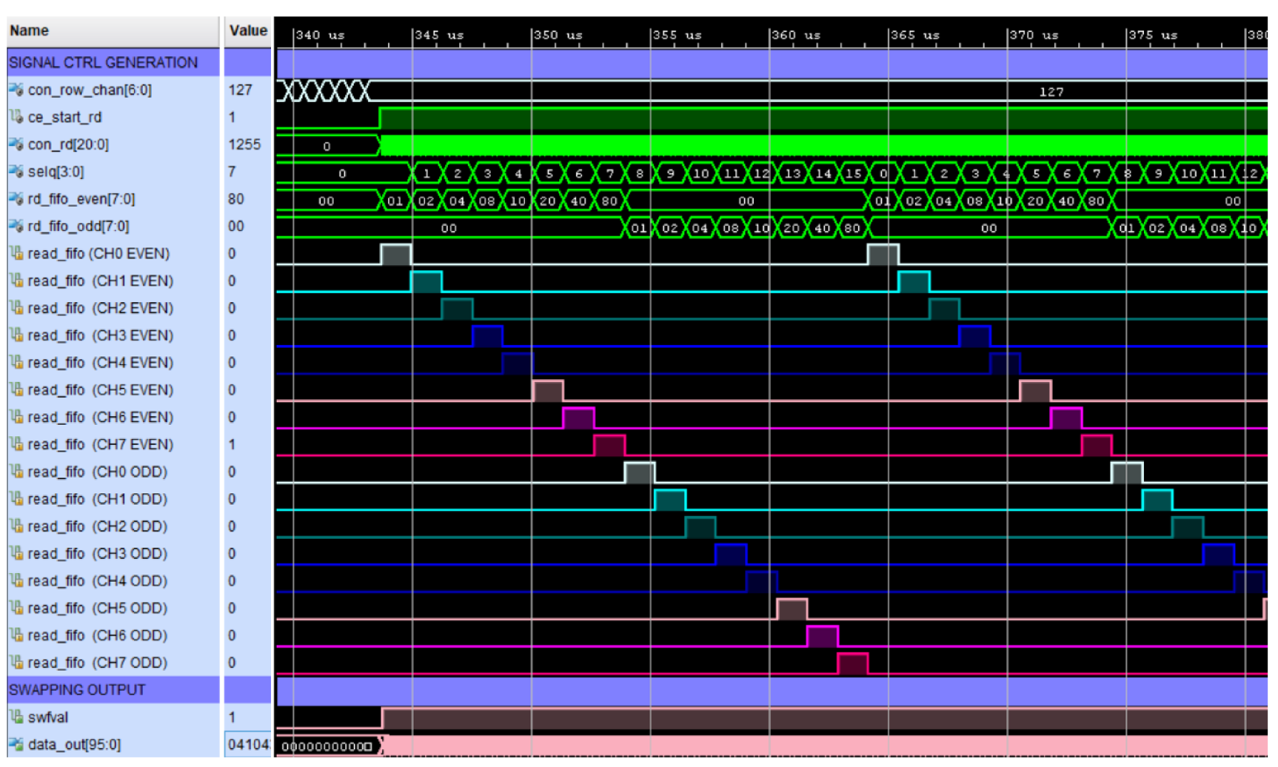
Figure 11 shows a simulation of the sequential reading of all FIFOs to form the correctly ordered data. The swapping module waits for enough data to be stored in the FIFOs to avoid any empty FIFO situation. This is ensured when the internal
con_row_chan counter reaches the value of 127 stored rows and then the ce_start_rd signal is set to high. This trigger activates the
con_rd counter which is used to generate
rd_fifo signals and the selection signal of the 16-to-1 multiplexer in
Figure 8. The decoding of the
con_rd counter bits is shown in
Table 4. Each
read_fifo signal in
Figure 11 remains high for 32 clock cycles because the 8-pixel data format takes that time to read the 512-pixel section of the row corresponding to its channel.
When
swfal is equal to one,
data_out provides the first 8-pixel data for row 0, then the following 8-pixel data and so on until 256 (in 32 clock cycles) and then the same with the other channels:
These signals are in pink colour in
Figure 11. Then, the submodule consecutively provides rows 1, 2, 3… until it reaches the
window_row_length defined by the selected RoI. The
data_out port supplies the image data arranged in rows-by-columns but with the data grouped in packets of 8 pixels (96 bits) as mentioned.
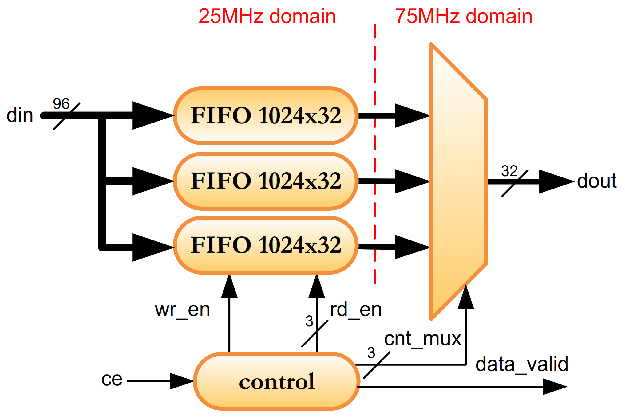
4.2. Packer Module
The packer module adapts the incoming 96-bit data (8 pixels) to 32-bit in order to send them via CoaXPress IF. It has been described using VHDL language and its interface is shown in
Figure 12. A brief description of each module port is also shown in
Table 5.
This module implements three 32 × 1024 FIFO to change the clock domain from 25 MHz to 75 MHz and a 3-to-1 multiplexer. This multiplexer selects 31 to 0 bits, 63 to 32 bits and 95 to 64 bits for each incoming data. A system control module generates read and write FIFO signals and the selection signal for the multiplexer. The detailed diagram of this module is shown in
Figure 13.
Figure 14 depicts a simulation of the packer operation. When
ce signal is set to high,
wr_en signal is set to high and the 8-pixel incoming data are distributed to the 3 FIFOs divided in a 32-pixel format as mentioned. These data are then sequentially read at 75 MHz in a totally sequential operation using
rd_en signals (in red). The data for the output port is generated by concatenating the outputs of the FIFOs using the
cnt_mux signal (in yellow). Thus, it can be seen that every 8 pixels are divided into 3 packets of 2 ⅔ pixels each (see values the
din and
dout orange signals).
4.3. Image_tx Module
It adapts the data for sending them via CoaXPress IF. The port interface of this module is depicted in
Figure 15.
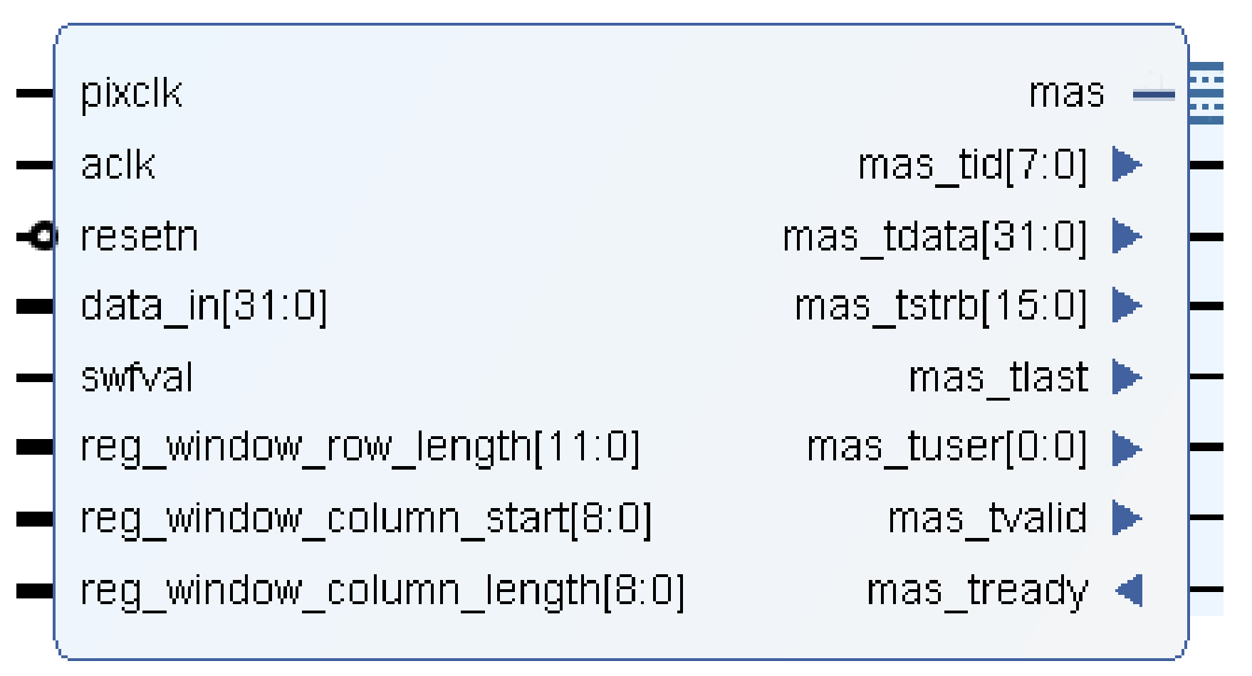
Swfval data acts as chip enable and
reg_window_row_length,
reg_window_column_start and
reg_window_column_length parameters are used to generate
mas_group signals. A brief description of each module port is also shown in
Table 6.
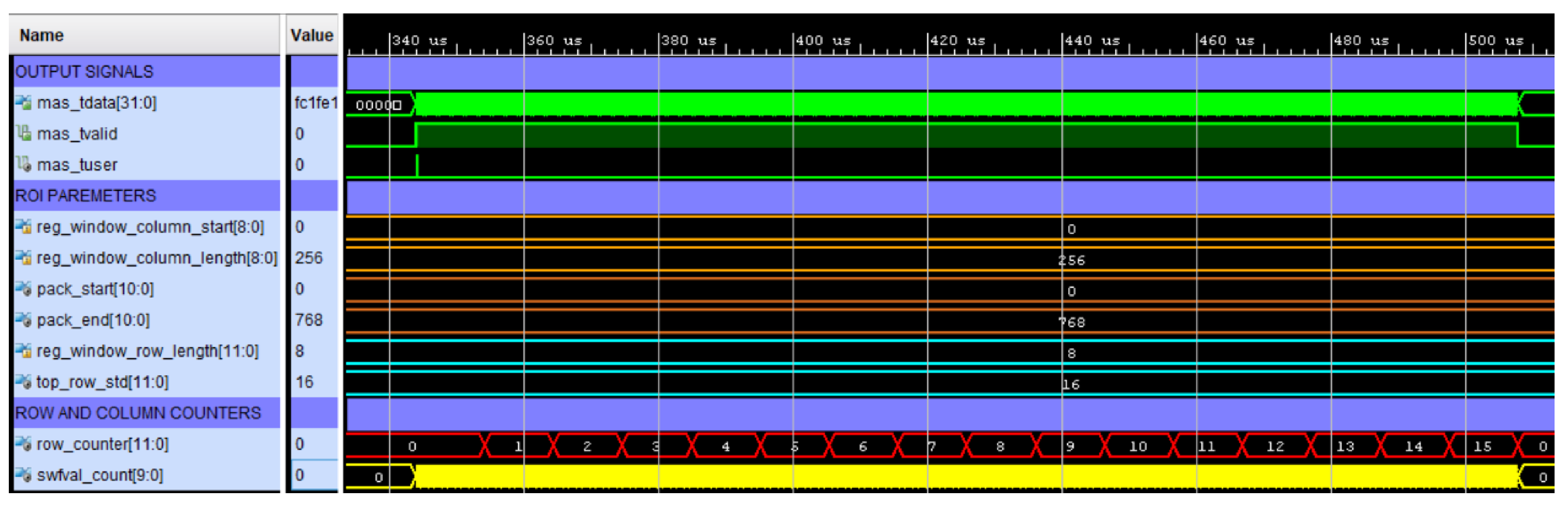
In this case, the reg_window_column_start and reg_window_column_length registers have only 9 bits as trimming the RoI by columns only allows multiples of 8, due to the limitation imposed by the 32-bit packet transmission channel. Thus, this module uses dividers to convert these registers into equivalent transmission packets. The image_tx module also implements two counters, named row_counter and swfval_count, which keep track of the rows and the packets of each row that are transmitted.
Figure 16 depicts a simulation of this module for a 16-rows image. When
swfal is equal to one, it generates a trigger (
mas_tuser signal), enable a strobe signal (
mas_tvalid) and the module sends packets to the CoaXPress IP through
mas_tdata signal (see green signals in
Figure 16). In this case, the
reg_window_column_length register is equal to 256. This is:
that is, all the columns in the image. Therefore, each row is made up of:
(see
top_row_std signal in cyan colour). When
row_counter counter reaches the value 16 and the
swfval_count counter reaches the value 768, all the image data has been transmitted, and the
mas_tvalid signal is disabled.
Figure 17 depicts a simulation of an image using a RoI with 16 rows and 512 columns. In this case,
reg_window_column_start is equal to 2 and
reg_window_column_length is 64. Performing the same calculations as in the previous case, now
pack_start signal is 16 and
pack_end is 6 + 192 = 198 (orange signals in
Figure 17). The module only sends packets that are within this range, in such a way that if the counter is less than 6 or greater than 198, the
mas_tvalid signal is disabled (see green signals).
5. Results
Firmware Image Ordering and Packing for TuMag Camera has been implemented using VHDL language. For this, the Artix-7 XC7A50T-2CSG325C device has been used. The code has been developed using Vivado 2017.4 for simulation, debugging and implementation. This module has been successfully integrated into the sensor driver and is now fully operational. The FPGA resources used by each of the three sub-modules are detailed in
Table 7.
It can be seen that the swapping submodule is the one that uses the most resources, mainly due to the relevant number and size of the modules it uses for ordering. In general, the most committed resource is memory (BRAM), used to configure the 16 FIFOs necessary to carry out the ordering operation (37.3%). However, the rest of the resources used by the sensor driver are used in control and configuration tasks and little additional memory is used.
Table 8 shows the latency of the imaging system. It can be seen that the greater latency of the system is due to the image ordering module.
Packer and
image_tx modules only handle data grouping and CoaXPress control signals, so the latency is much lower compared to the
swapping module.
The image ordering algorithm was implemented using software tools, in order to obtain the improvement achieved in terms of computational time. For the computational time analysis in Matlab and C++, we used a Dell Vostro PC with the following characteristics: Windows 7 Professional 64 bits, Intel Core i7 860/2.8 GHz, 20 Gb RAM DDR3. The execution time is 37.469 ms using Matlab and 277.57 µs using C++.
The results show the improvement in the computational time of the FPGA implementation over the Matlab and C++ simulations. The speed-up is 455 in comparison with the Matlab implementation and 3.37 in comparison with the C++ implementation.
As we have mentioned previously, GSENSE400 is a relatively new image sensor with high dynamic range, high sensitivity and low noise. The few developments that they have currently been implemented for this sensor do not include the Image Ordering and Packing algorithm in the read-out electronic and this task is performed by software at the host [
32,
33,
34,
35]. Also, the FPGA devices in these implementations are older: Spartan-6, Virtex-4 and Virtex-5 respectively. Our implementation uses an Artix-7, a FPGA of the 7-series family, with more resources and new components. This increase in performance allows the integration of more functionalities, such as the swapping module. Spartan-6, Virtex-4, and Virtex-5 implementations are developed using the deprecated ISE development environment. Our implementation using an Artix-7 FPGA has been developed using Vivado, the current Xilinx tool. This makes it easy to upgrade the FPGA firmware with new IP libraries.
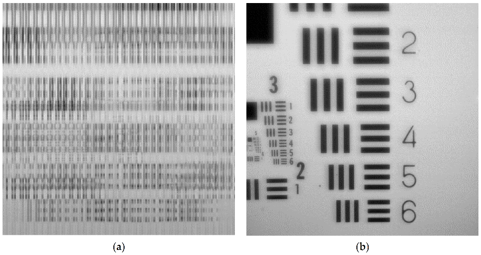
Figure 18 shows the results of acquiring an image with the prototype in which the USAF (United States Air Force) resolution test chart has been used. The image on the left has been taken without including the swapping module in the firmware (unordered image). In the image on the left, the swapping module has been included in the firmware and the image obtained in the frame grabber is correctly arranged in the desired rows by columns format (ordered image).
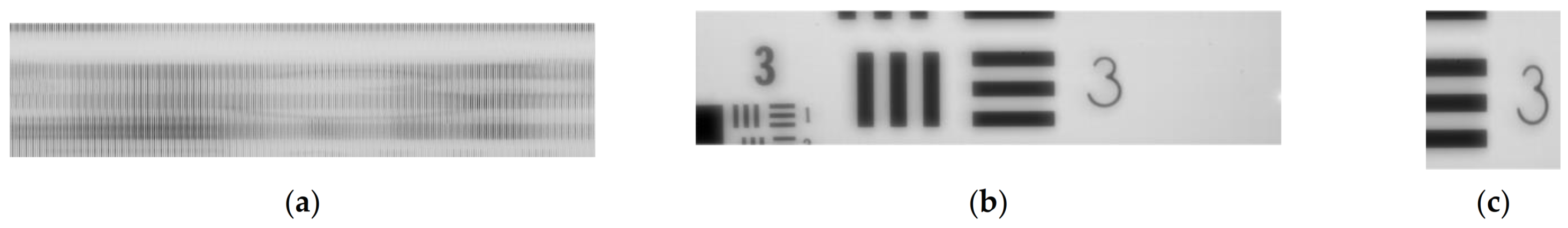
Figure 19 depicts the result of selecting a smaller size in image rows using
reg_window_row_start equal to 512 and
reg_window_row_length equal to 512. At left, unordered image is depicted and at centre, ordered image is depicted. As mentioned, the sensor does not allow the selection of a range of columns, so the image at right in
Figure 19 comes from the same captured image as for image at centre. In this case,
reg_window_column_start and
reg_window_column_length registers have been used to select the range of columns to be sent through the CoaXPress interface in the
image_tx module, as explained in
Section 4.3. In this case,
reg_window_column_start equal to 128 and
reg_window_column_length equal to 64 has been used to obtain the sub-image at right.
In the development of the firmware, special attention has been paid to the synchronism of the signals between the modules. Due to the characteristics of the sensor output format, the loss of a pixel causes a misalignment of a pixel, but also the disorder between odd and even rows. This effect can be seen in the images in
Figure 20 that were obtained during the development of the firmware. The detail in the image on the left shows unwanted line clutter. In the image on the right the timing has been corrected and is displayed correctly.
6. Conclusions and Future Work
The camera firmware has been successfully debugged. This firmware includes image ordering and image packing. The image ordering is done correctly without synchronism or line spacing problems. It also adapts the data for sending them via CoaXPress IF. This uses relatively few FPGA resources, so the rest of the camera control firmware can be implemented without resource issues.
Efforts are currently focused on the development of DPU control firmware. The camera prototype must also be tested in a vacuum chamber in which the temperature will be modified in the range of −20 to 40-Celsius degrees.
Before the flight, rigorous and demanding processes will be carried out to validate the performance of TuMag camera in the laboratory. For this, the extreme conditions of the space environment are simulated on multiple testbenches, which are located into different research center of TuMag project. Consequently, some instruments including the camera and the host/tester must be transported to each center for mount different experimental setups. The transport of this equipment involves risks in its integrity, and requires human and economic project resources to execute the necessary logistics. It is possible to simplify the number of equipment to be transported and reduce the mounting time of experimental setups if each research center has the same host/tester installed on its testbench. In this case, we assume that transportation will only be required for the camera. So, another step consists in the design and implementation of a TuMag camera tester using Eurasys Coaxlink Quad frame grabber and EGenTL/EGrabber libraries for use in multiple testbenches.


