
Behavioral Model of Silicon Photo-Multipliers Suitable for Transistor-Level Circuit Simulation


Abstract
:1. Introduction
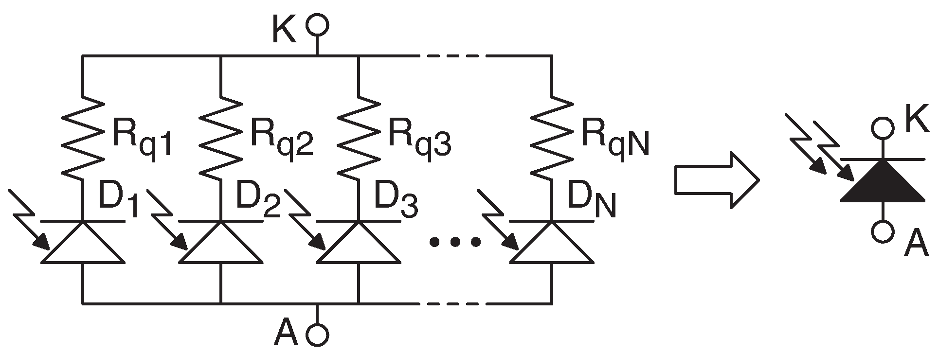
2. Traditional SiPM Device Modeling
- 1.
- 2.
- Since the photon arrival is emulated by the current generator, , the model cannot self-quench the avalanche of the firing diode (specifically, either the designer uses a complex APD model, such as the one in [18], or the APD model requires that the impulse of the avalanche current is calculated a priori);
- 3.
- No statistical phenomena (i.e., dark-count or after-pulsing [17]) are considered in the model.
- 1.
- Multiple concurrent firing cells;
- 2.
- Avalanche self-quenching;
- 3.
- Emulation of statistical phenomena (i.e., dark-count and after-pulsing effects).
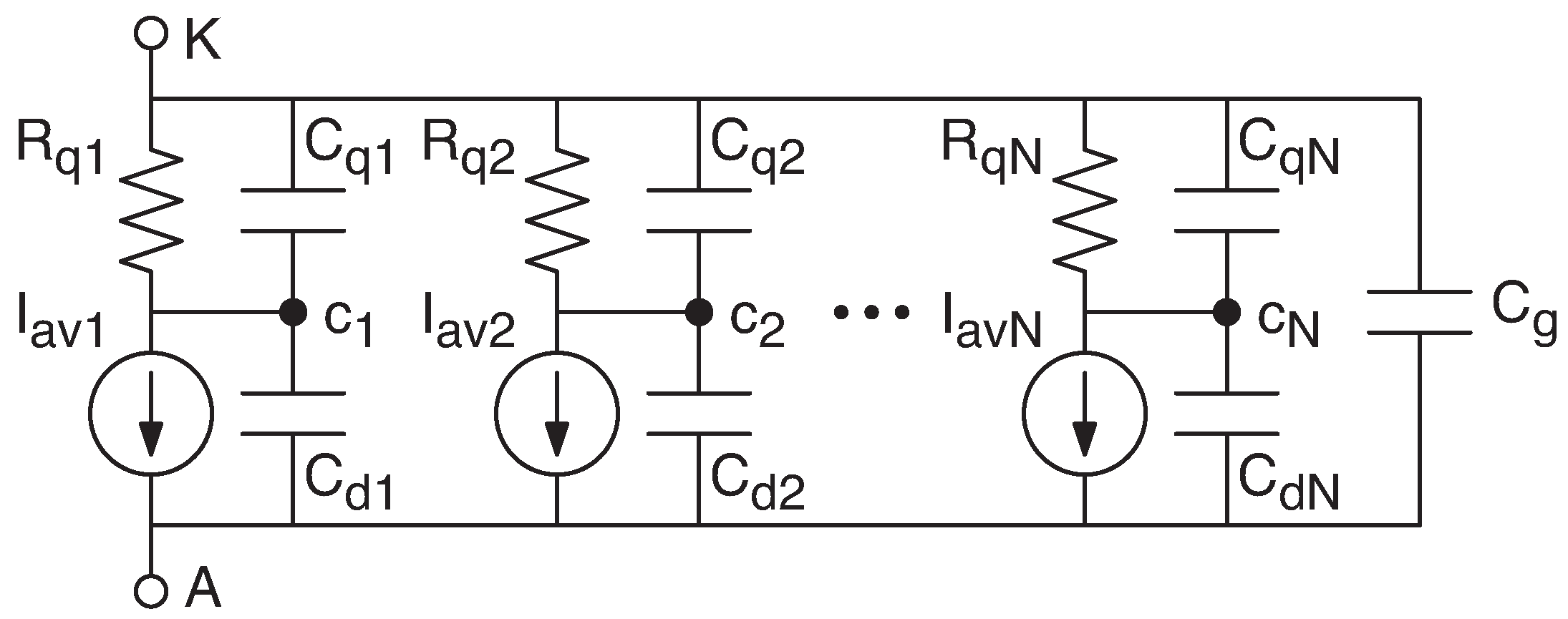
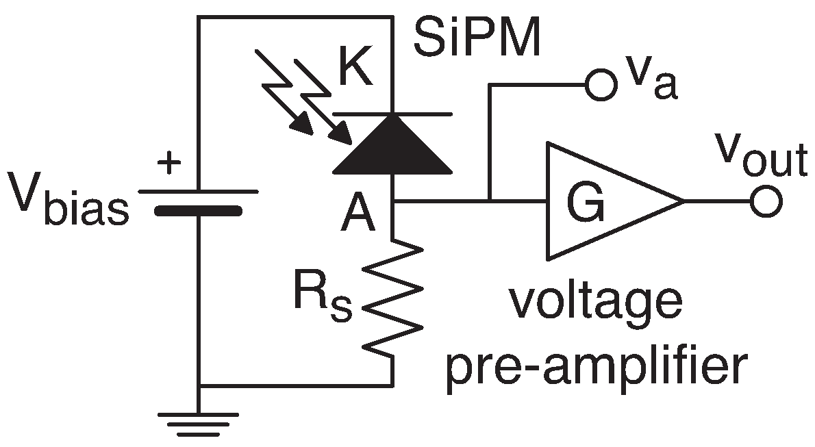
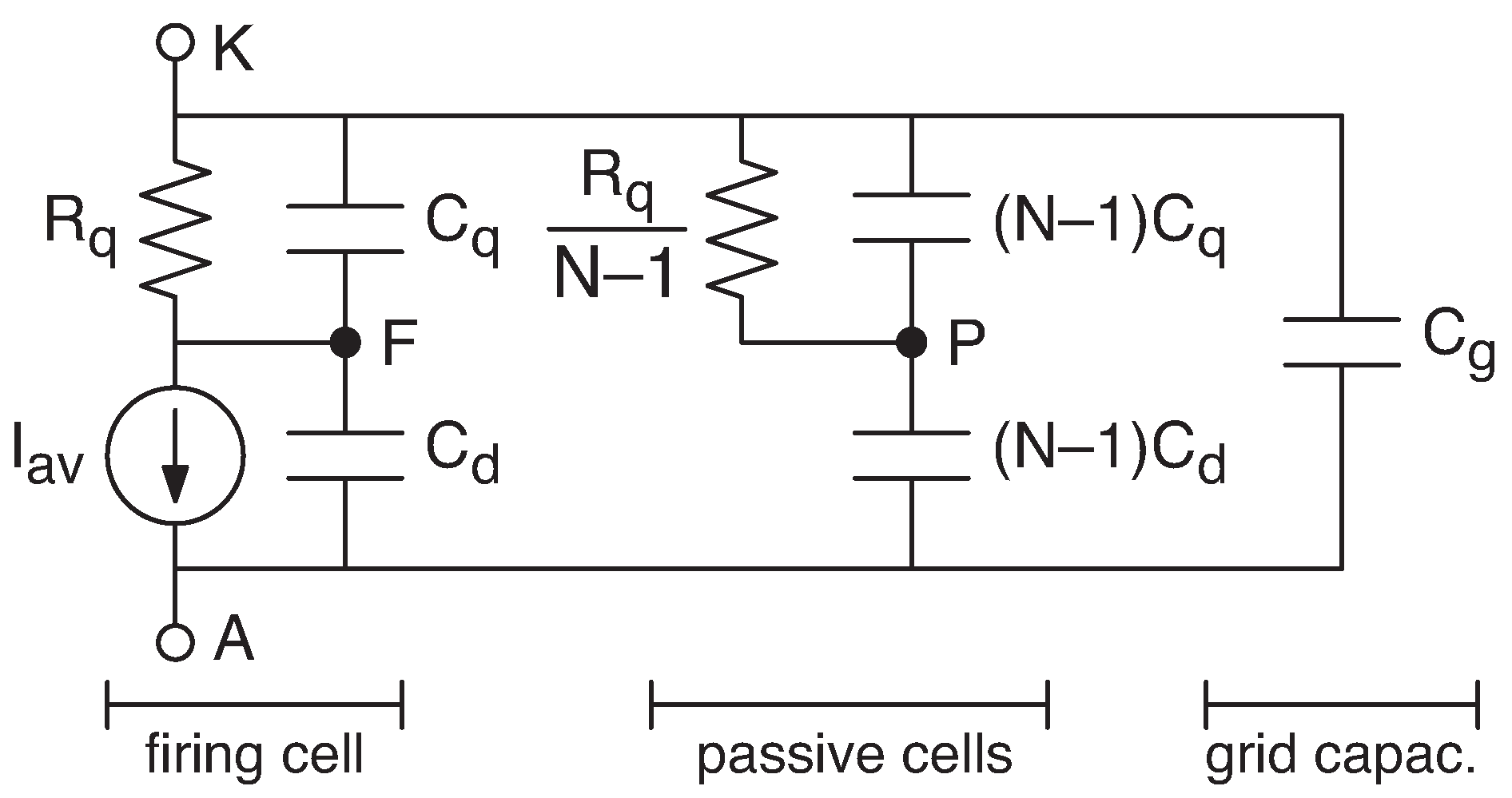
3. SiPM Electrical Modeling
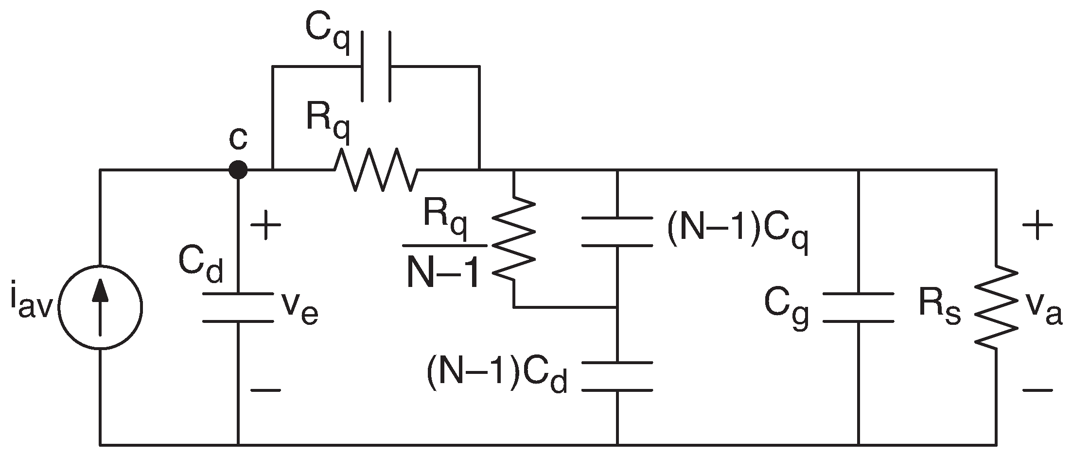
3.1. Equivalent Circuit Transfer Function
3.2. Time Response to a Single Firing APD
4. SiPM Statistical Modeling
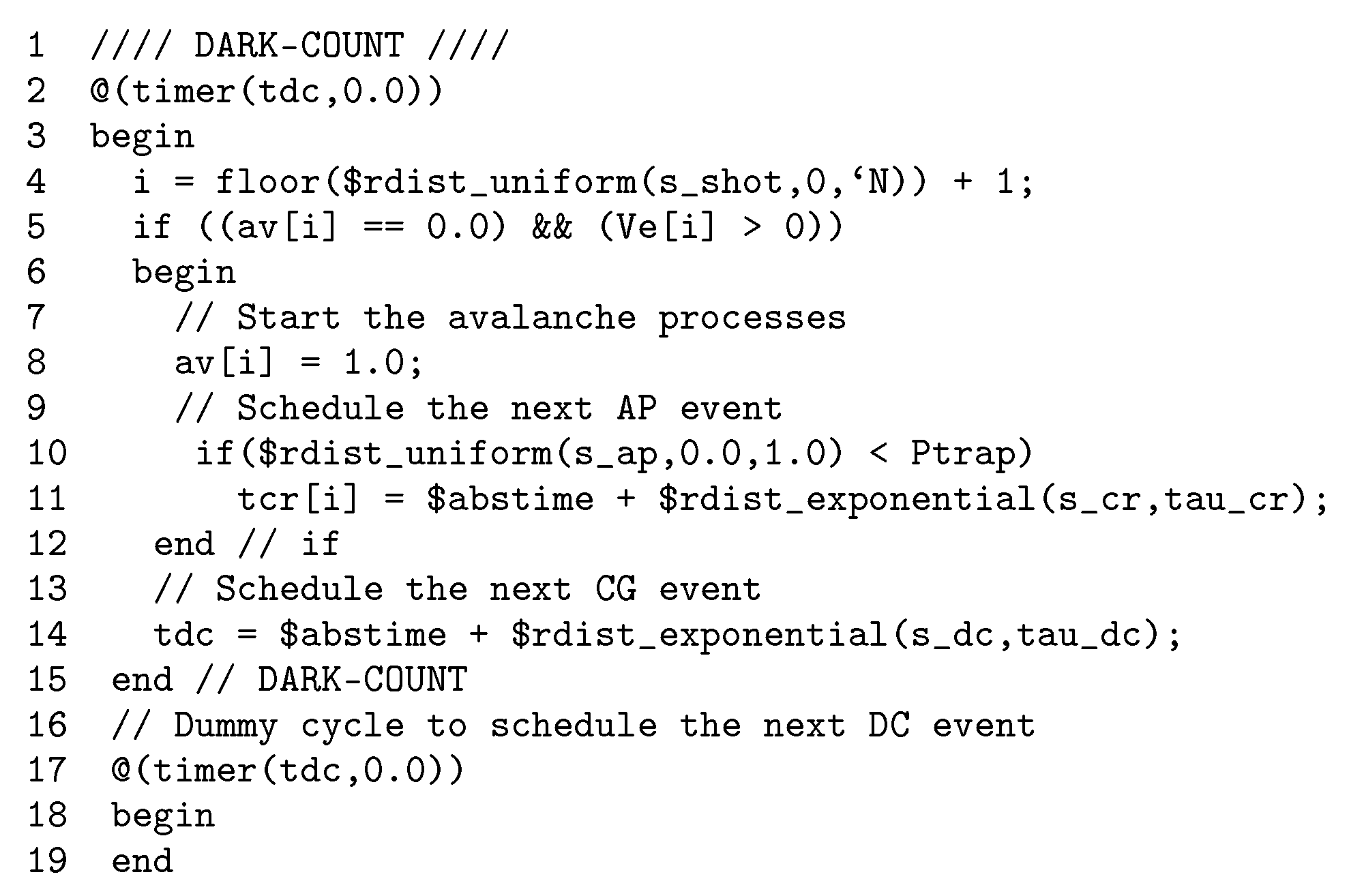
4.1. Dark-Count
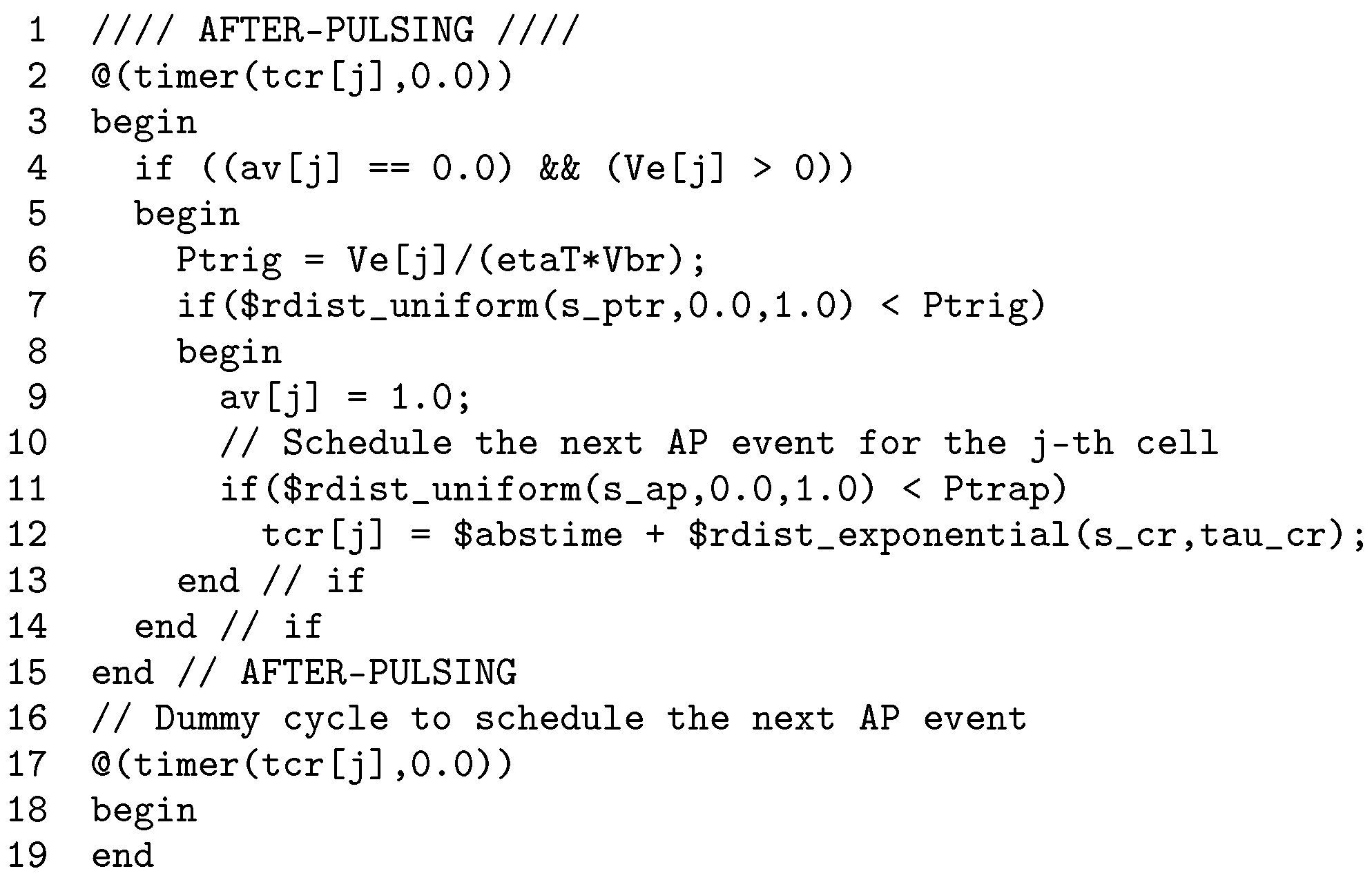
4.2. Carrier Release and after-Pulsing
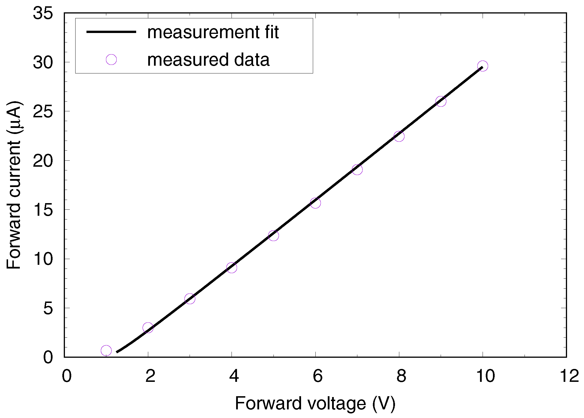
5. Parameter Extraction
5.1. Electrical Model
5.2. Statistical Model
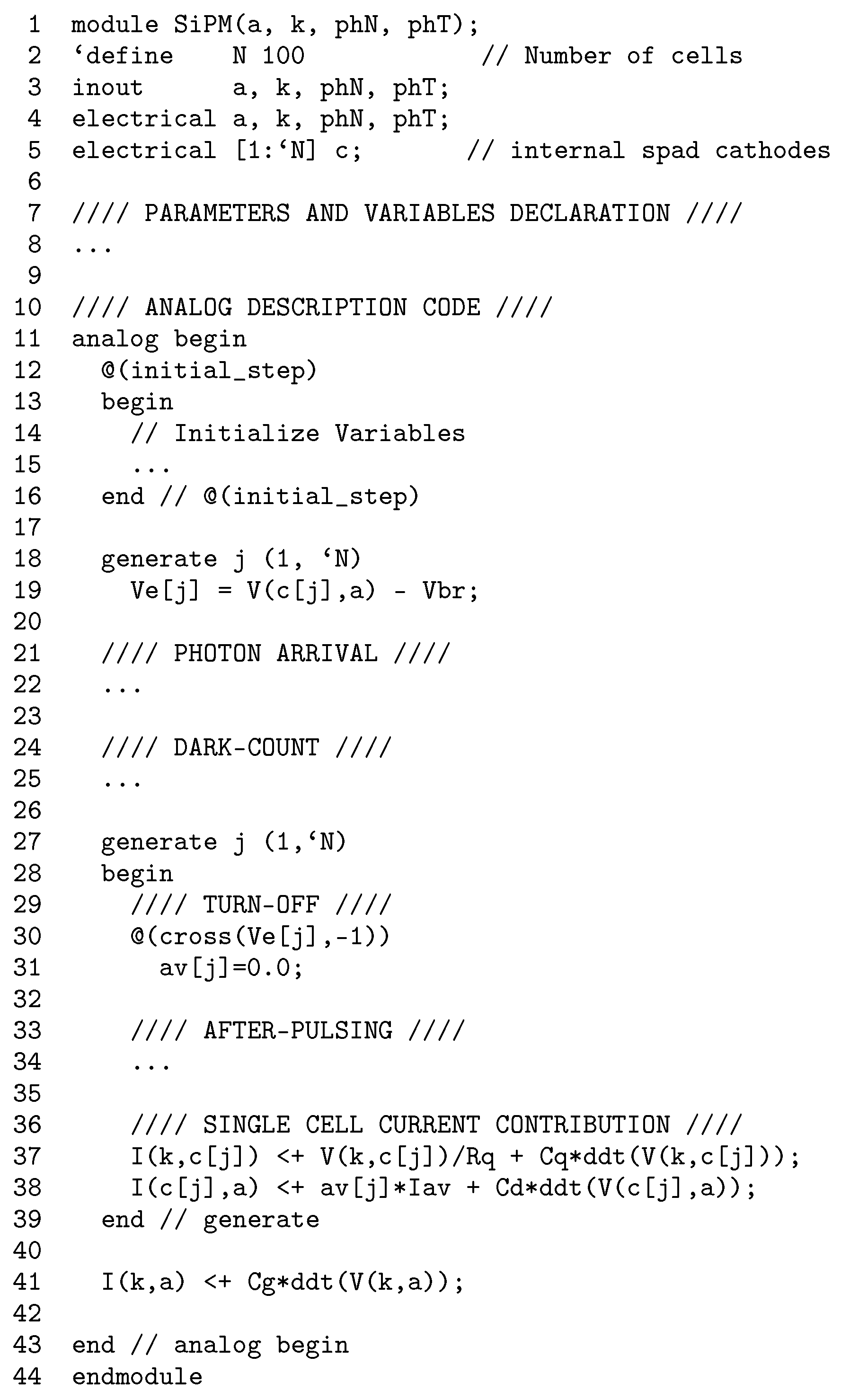
6. Verilog-a Model
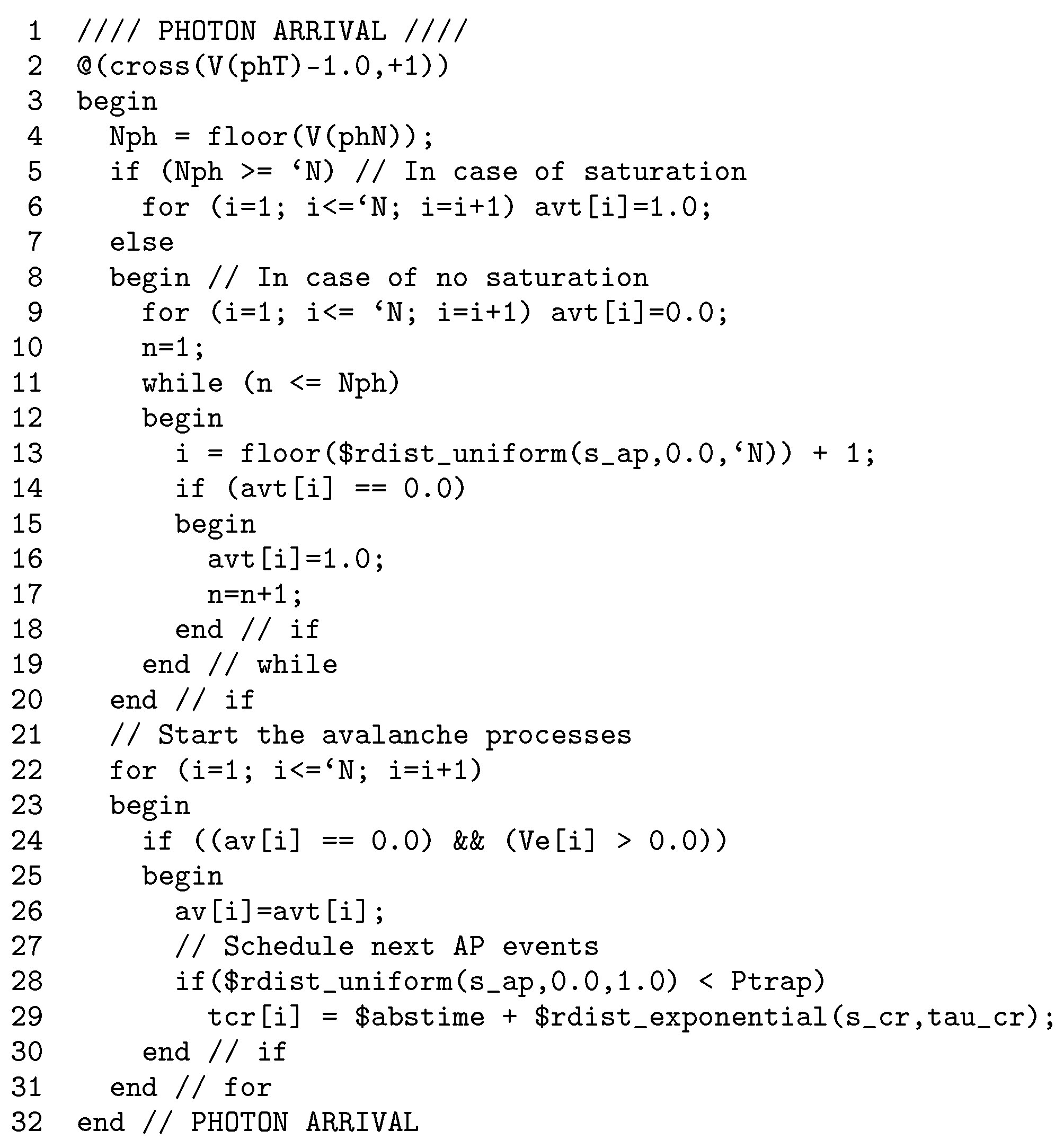
6.1. Photon Arrival
6.2. Dark-Count
6.3. After-Pulsing
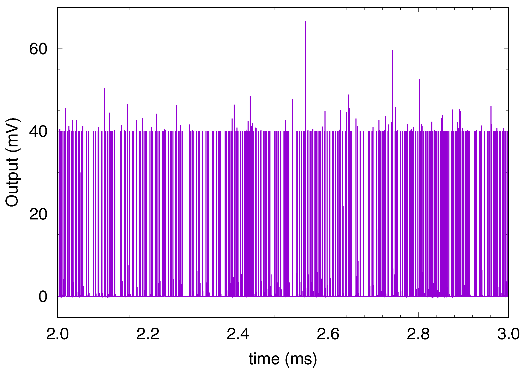
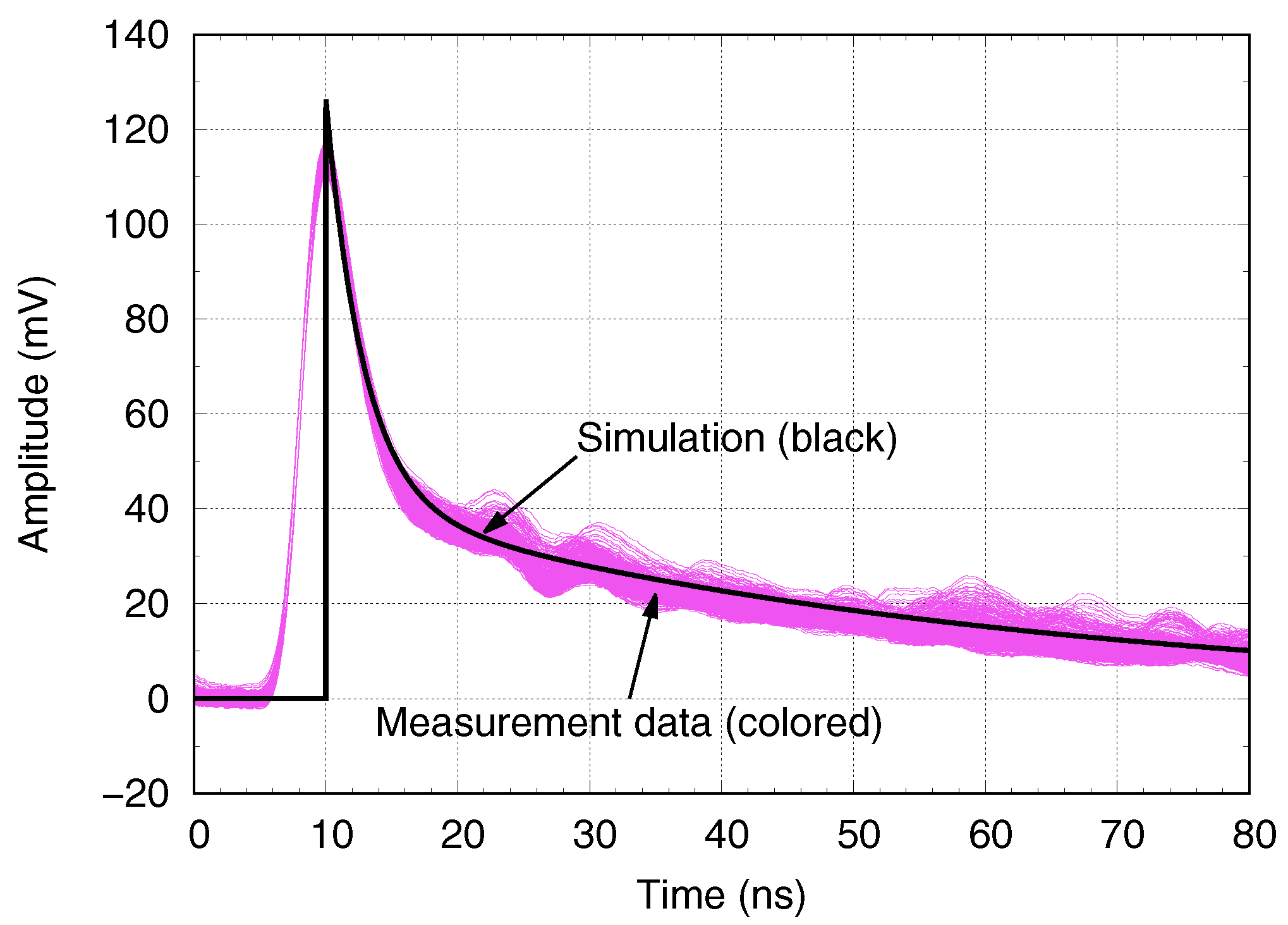
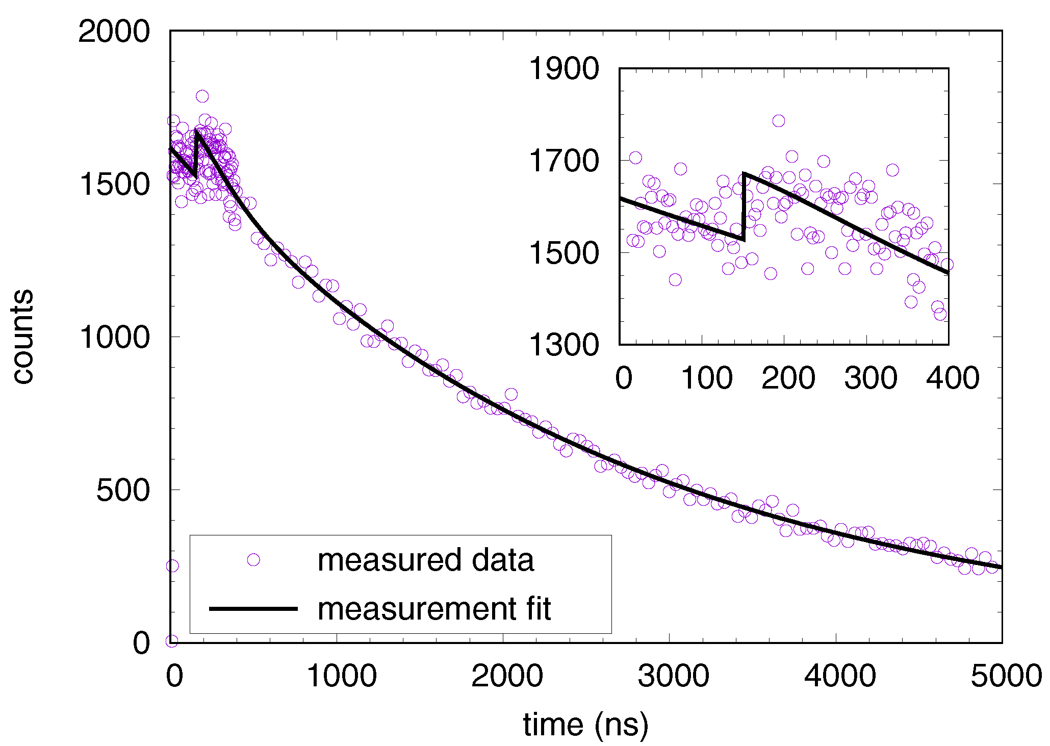
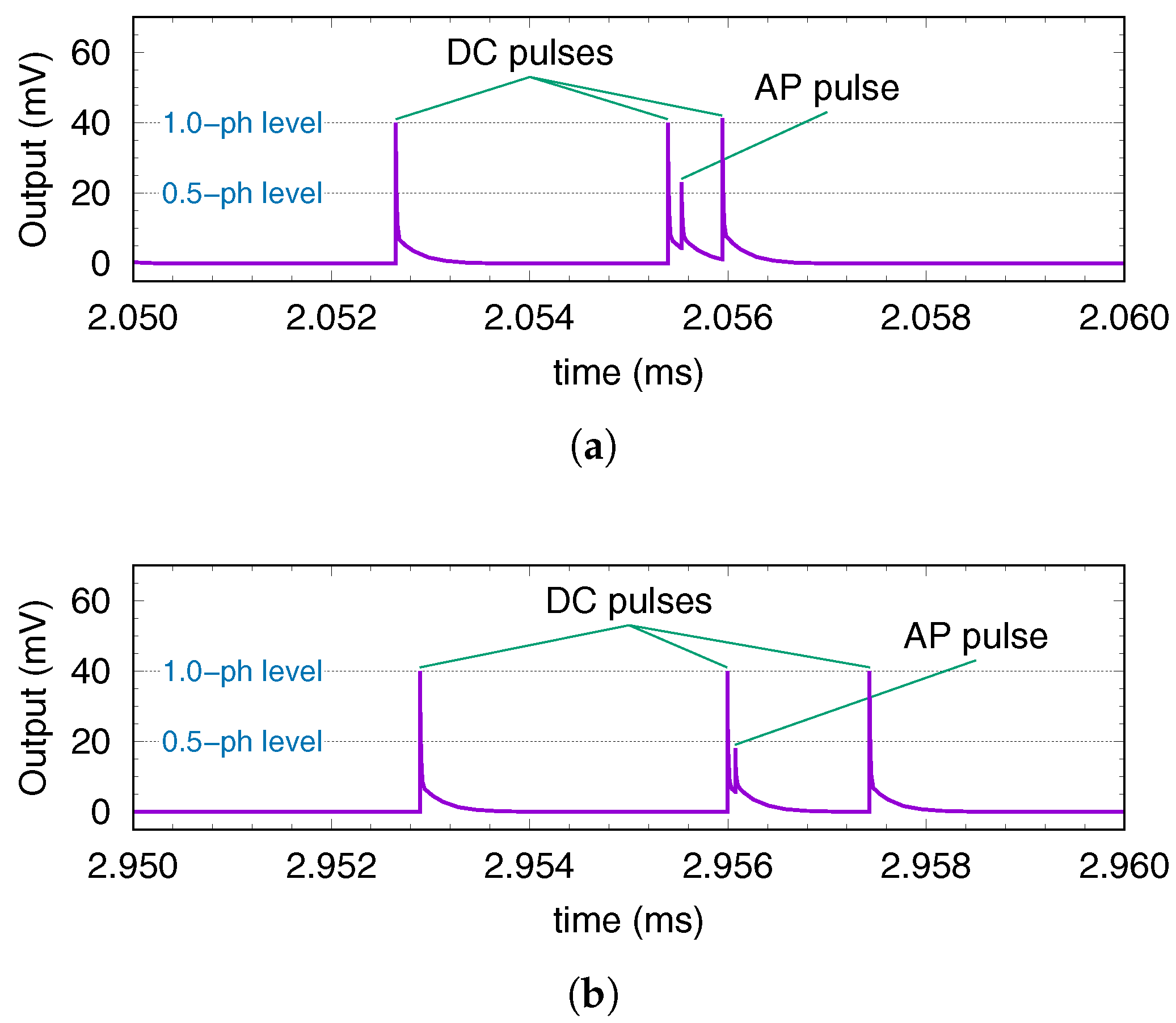
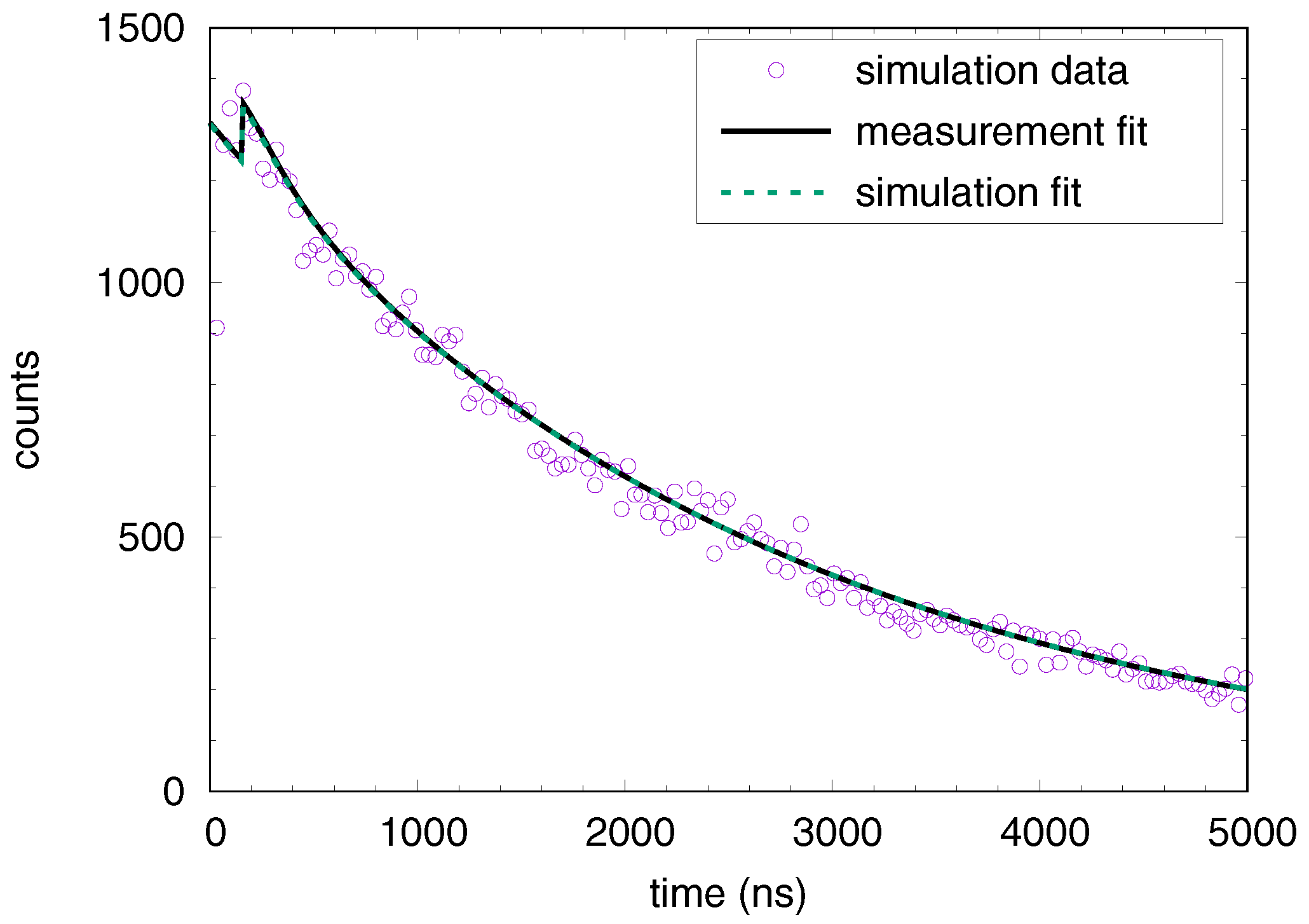
7. Model Validation
8. Conclusions
Author Contributions
Funding
Data Availability Statement
Conflicts of Interest
References
- Finocchiaro, P.; Pappalardo, A.; Cosentino, L.; Belluso, M.; Billotta, S.; Bonanno, G.; Carbone, B.; Condorelli, G.; Di Mauro, S.; Fallica, G.; et al. Characterization of a Novel 100-Channel Silicon Photomultiplier—Part I: Noise. IEEE Trans. Electron Devices 2008, 55, 2757–2764. [Google Scholar] [CrossRef]
- Finocchiaro, P.; Pappalardo, A.; Cosentino, L.; Belluso, M.; Billotta, S.; Bonanno, G.; Carbone, B.; Condorelli, G.; Di Mauro, S.; Fallica, G.; et al. Characterization of a Novel 100-Channel Silicon Photomultiplier—Part II: Charge and Time. IEEE Trans. Electron Devices 2008, 55, 2765–2773. [Google Scholar] [CrossRef]
- Stoppa, D.; Pancheri, L.; Scandiuzzo, M.; Gonzo, L.; Dalla Betta, G.F.; Simoni, A. A CMOS 3-D Imager Based on Single Photon Avalanche Diode. IEEE Trans. Circuits Syst. I 2007, 54, 4–12. [Google Scholar] [CrossRef]
- Gersbach, M.; Maruyama, Y.; Trimananda, R.; Fishburn, M.W.; Stoppa, D.; Richardson, J.A.; Walker, R.; Henderson, R.; Charbon, E. A Time-Resolved, Low-Noise Single-Photon Image Sensor Fabricated in Deep-Submicron CMOS Technology. IEEE J. Solid-State Circuits 2012, 47, 1394–1407. [Google Scholar] [CrossRef]
- Pappalardo, A.; Cosentino, L.; Barbagallo, M.; Marchetta, C.; Scirè, C.; Scirè, S.; Vecchio, G.; Finocchiaro, P. Silicon photomultipliers with scintillator for thermal neutron detection. IEEE J. Sel. Top. Quantum Electron. 2014, 20, 1–7. [Google Scholar] [CrossRef]
- Pappalardo, A.; Cosentino, L.; Scirè, C.; Scirè, S.; Vecchio, G.; Finocchiaro, P. Low-cost radioactivity monitoring with scintillating fibers and silicon photomultipliers. Opt. Eng. 2014, 53. [Google Scholar] [CrossRef]
- Trigilio, P.; Busca, P.; Quaglia, R.; Occhipinti, M.; Fiorini, C. A SiPM-Readout ASIC for SPECT Applications. IEEE Trans. Radiat. Plasma Med. Sci. 2018, 2, 404–410. [Google Scholar] [CrossRef]
- Zhang, H.; Fan, P.; Wang, S.; Xia, Y.; Xu, T.; Wei, Q.; Lu, W.; Wu, Z.; Liu, Y.; Ma, T. Design and Performance Evaluation of a BGO + SiPM Detector for High-Energy Prompt Gamma Imaging in Proton Therapy Monitoring. IEEE Trans. Radiat. Plasma Med. Sci. 2020, 4, 184–193. [Google Scholar] [CrossRef]
- Braga, L.H.C.; Gasparini, L.; Grant, L.; Henderson, R.K.; Massari, N.; Perenzoni, M.; Stoppa, D.; Walker, R. A Fully Digital 8 × 16 SiPM Array for PET Applications With Per-Pixel TDCs and Real-Time Energy Output. IEEE J. Solid-State Circ. 2014, 49, 301–314. [Google Scholar] [CrossRef]
- Cosentino, L.; Finocchiaro, P.; Pappalardo, A.; Garibaldi, F. Assessment of a high-resolution candidate detector for prostate time-of-flight positron emission tomography. Rev. Sci. Instrum. 2012, 83, 114301. [Google Scholar] [CrossRef] [Green Version]
- Cosentino, L.; Finocchiaro, P.; Pappalardo, A.; Garibaldi, F. Characterization of a scintillating mini-detector for time-of-flight positron emission tomography with depth-of-interaction. Rev. Sci. Instrum. 2012, 83, 084302. [Google Scholar] [CrossRef]
- Tétrault, M.; Corbeil Therrien, A.; Lemaire, W.; Fontaine, R.; Pratte, J. TDC Array Tradeoffs in Current and Upcoming Digital SiPM Detectors for Time-of-Flight PET. IEEE Trans. Nucl. Sci. 2017, 64, 925–932. [Google Scholar] [CrossRef]
- Eshkoli, A.; Nemirovsky, Y. Characterization and Architecture of Monolithic N+P-CMOS-SiPM Array for ToF Measurements. IEEE Trans. Instrum. Meas. 2021, 70, 1–9. [Google Scholar] [CrossRef]
- Akamatsu, G.; Takyu, S.; Yoshida, E.; Iwao, Y.; Tashima, H.; Nishikido, F.; Yamaya, T. Evaluation of a Hamamatsu TOF-PET Detector Module with 3.2 mm Pitch LFS Scintillators and a 256-channel SiPM Array. IEEE Trans. Radiat. Plasma Med. Sci. 2021. [Google Scholar] [CrossRef]
- Ahmed, Z.; Singh, R.; Ali, W.; Faulkner, G.; O’Brien, D.; Collins, S. A SiPM-Based VLC Receiver for Gigabit Communication Using OOK Modulation. IEEE Photon. Technol. Lett. 2020, 32, 317–320. [Google Scholar] [CrossRef]
- Meng, X.; Cunningham, D.G.; White, I.H.; Penty, R.V. SPAD-Array Contention Signal and Noise Model Suitable for Multilevel Modulation Schemes With Signal Processing. IEEE Access 2021, 9, 48483–48500. [Google Scholar] [CrossRef]
- Cova, S.; Ghioni, M.; Lacaita, A.; Samori, C.; Zappa, F. Avalanche photodiodes and quenching circuits for single-photon detection. Appl. Opt. 1996, 35, 1956–1976. [Google Scholar] [CrossRef] [PubMed]
- Dalla Mora, A.; Tosi, A.; Tisa, S.; Zappa, F. Single-Photon Avalanche Diode Model for Circuit Simulations. IEEE Photon. Technol. Lett. 2007, 19, 1922–1924. [Google Scholar] [CrossRef] [Green Version]
- Mita, R.; Palumbo, G. High-Speed and Compact Quenching Circuit for Single-Photon Avalanche Diodes. IEEE Trans. Instrum. Meas. 2008, 57, 543–547. [Google Scholar] [CrossRef]
- Giustolisi, G.; Grasso, A.D.; Palumbo, G. Integrated Quenching-and-Reset Circuit for Single-Photon Avalanche Diodes. IEEE Trans. Instrum. Meas. 2015, 64, 271–277. [Google Scholar] [CrossRef]
- Mita, R.; Palumbo, G.; Fallica, P.G. Accurate model for single-photon avalanche diodes. IET Circuits Devices Syst. 2008, 2, 207–212. [Google Scholar] [CrossRef]
- Giustolisi, G.; Mita, R.; Palumbo, G. Behavioral modeling of statistical phenomena of single-photon avalanche diodes. Int. J. Circ. Theor. Appl. 2012, 40, 661–679. [Google Scholar] [CrossRef]
- Pavlov, N.; Mæhlum, G.; Meier, D. Gamma Spectroscopy using a Silicon Photomultiplier and a Scintillator. In Proceedings of the IEEE Nuclear Science Symposium Conference Record, Fajardo, PR, USA, 23–29 October 2005; Volume 1, pp. 173–180. [Google Scholar] [CrossRef]
- Corsi, F.; Marzocca, C.; Perrotta, A.; Dragone, A.; Foresta, M.; Del Guerra, A.; Marcatili, S.; Llosa, G.; Collazzuol, G.; Dalla Betta, G.; et al. Electrical Characterization of Silicon Photo-Multiplier Detectors for Optimal Front-End Design. In Proceedings of the 2006 IEEE Nuclear Science Symposium Conference Record (NSS/MIC), San Diego, CA, USA, 29 October–1 November 2006; Volume 2, pp. 1276–1280. [Google Scholar] [CrossRef]
- Seifert, S.; van Dam, H.T.; Huizenga, J.; Vinke, R.; Dendooven, P.; Löhner, H.; Schaart, D.R. Simulation of Silicon Photomultiplier Signals. IEEE Trans. Nucl. Sci. 2009, 56, 3726–3733. [Google Scholar] [CrossRef]
- Marano, D.; Belluso, M.; Bonanno, G.; Billotta, S.; Grillo, A.; Garozzo, S.; Romeo, G.; Catalano, O.; La Rosa, G.; Sottile, G.; et al. Silicon Photomultipliers Electrical Model Extensive Analytical Analysis. IEEE Trans. Nucl. Sci. 2014, 61, 23–34. [Google Scholar] [CrossRef]
- Marano, D.; Bonanno, G.; Garozzo, S.; Grillo, A.; Romeo, G. New Improved Model and Accurate Analytical Response of SiPMs Coupled to Read-Out Electronics. IEEE Sens. J. 2016, 16, 19–21. [Google Scholar] [CrossRef]
- Corsi, F.; Foresta, M.; Marzocca, C.; Matarrese, G.; Del Guerra, A. Current-mode front-end electronics for silicon photo-multiplier detectors. In Proceedings of the 2007 2nd International Workshop on Advances in Sensors and Interface (IWASI), Bari, Italy, 26–27 June 2007; pp. 1–6. [Google Scholar] [CrossRef]
- Retière, F. MPPC Response Simulation and High Speed Readout Optimization. In Proceedings of the 2009 IEEE Nuclear Science Symposium Conference Record (NSS/MIC), Orlando, FL, USA, 24 October–1 November 2009; pp. 2197–2200. [Google Scholar] [CrossRef]
- Corsi, F.; Dragone, A.; Marzocca, C.; Del Guerra, A.; Delizia, P.; Dinu, N.; Piemonte, C.; Boscardin, M.; Dalla Betta, G. Modelling a silicon photomultiplier (SiPM) as a signal source for optimum front-end design. Nucl. Instrum. Methods Phys. Res. A 2007, 572, 416–418. [Google Scholar] [CrossRef]
- Marano, D.; Bonanno, G.; Garozzo, S.; Grillo, A.; Romeo, G. A New Simple and Effective Procedure for SiPM Electrical Parameter Extraction. IEEE Sens. J. 2016, 16, 3620–3626. [Google Scholar] [CrossRef]
- Giustolisi, G.; Palumbo, G.; Finocchiaro, P.; Pappalardo, A. A simple extraction procedure for determining the electrical parameters in Silicon Photomultipliers. In Proceedings of the 2013 European Conference on Circuit Theory and Design (ECCTD), Dresden, Germany, 8–12 September 2013. [Google Scholar] [CrossRef]
- Giustolisi, G.; Palumbo, G.; Finocchiaro, P.; Pappalardo, A. Verilog-a modeling of Silicon Photo-Multipliers. In Proceedings of the 2016 IEEE International Symposium on Circuits and Systems (ISCAS), Montreal, QC, Canada, 22–25 May 2016; pp. 1270–1273. [Google Scholar] [CrossRef]
- Sciacca, E.; Giudice, A.C.; Delfo Sanfilippo, F.Z.; Lombardo, S.; Consentino, R.; Di Franco, C.; Ghioni, M.; Fallica, G.; Bonanno, G.; Cova, S.; et al. Silicon Planar Technology for Single-Photon Optical Detectors. IEEE Trans. Electron Devices 2003, 50, 918–925. [Google Scholar] [CrossRef]
- Cova, S.; Lacaita, A.; Ripamonti, G. Trapping Phenomena in Avalanche Photodiodes on Nanosecond Scale. IEEE Electron Device Lett. 1991, 12, 685–687. [Google Scholar] [CrossRef]
- Gallina, G.; Retière, F.; Giampa, P.; Kroeger, J.; Margetak, P.; Mamahit, S.B.; Croix, A.D.; Edaltafar, F.; Martin, L.; Massacret, N.; et al. Characterization of SiPM Avalanche Triggering Probabilities. IEEE Trans. Electron Devices 2019, 66, 4228–4234. [Google Scholar] [CrossRef]
- Dautet, H.; Deschamps, P.; Dion, B.; MacGregor, A.D.; MacSween, D.; McIntyre, R.J.; Trottier, C.; Webb, P.P. Photon counting techniques with silicon avalanche photodiodes. Appl. Opt. 1993, 32, 3894–3900. [Google Scholar] [CrossRef] [PubMed] [Green Version]
- Ghioni, M.; Cova, S.; Zappa, F.; Samori, C. Compact active quenching circuit for fast photon counting with avalanche photodiodes. Rev. Sci. Instrum. 1996, 67, 2448–3440. [Google Scholar] [CrossRef] [Green Version]
- Coram, G.J. How to (and how not to) write a compact model in Verilog-A. In Proceedings of the 2004 IEEE International Behavioral Modeling and Simulation Conference, San Jose, CA, USA, 22–22 October 2004; pp. 97–106. [Google Scholar] [CrossRef]


| Parameter | Value |
|---|---|
| Parameter | Value |
|---|---|
| Parameter | Value |
|---|---|
| Parameter | Value |
|---|---|
| Parameter | Value |
|---|---|
Publisher’s Note: MDPI stays neutral with regard to jurisdictional claims in published maps and institutional affiliations. |
© 2021 by the authors. Licensee MDPI, Basel, Switzerland. This article is an open access article distributed under the terms and conditions of the Creative Commons Attribution (CC BY) license (https://creativecommons.org/licenses/by/4.0/).
Share and Cite
Giustolisi, G.; Finocchiaro, P.; Pappalardo, A.; Palumbo, G. Behavioral Model of Silicon Photo-Multipliers Suitable for Transistor-Level Circuit Simulation. Electronics 2021, 10, 1551. https://doi.org/10.3390/electronics10131551
Giustolisi G, Finocchiaro P, Pappalardo A, Palumbo G. Behavioral Model of Silicon Photo-Multipliers Suitable for Transistor-Level Circuit Simulation. Electronics. 2021; 10(13):1551. https://doi.org/10.3390/electronics10131551
Chicago/Turabian StyleGiustolisi, Gianluca, Paolo Finocchiaro, Alfio Pappalardo, and Gaetano Palumbo. 2021. "Behavioral Model of Silicon Photo-Multipliers Suitable for Transistor-Level Circuit Simulation" Electronics 10, no. 13: 1551. https://doi.org/10.3390/electronics10131551
APA StyleGiustolisi, G., Finocchiaro, P., Pappalardo, A., & Palumbo, G. (2021). Behavioral Model of Silicon Photo-Multipliers Suitable for Transistor-Level Circuit Simulation. Electronics, 10(13), 1551. https://doi.org/10.3390/electronics10131551