
A Novel Multilevel Controller


Abstract
:1. Introduction
2. Analysis of the Novel Nine-Level Topology
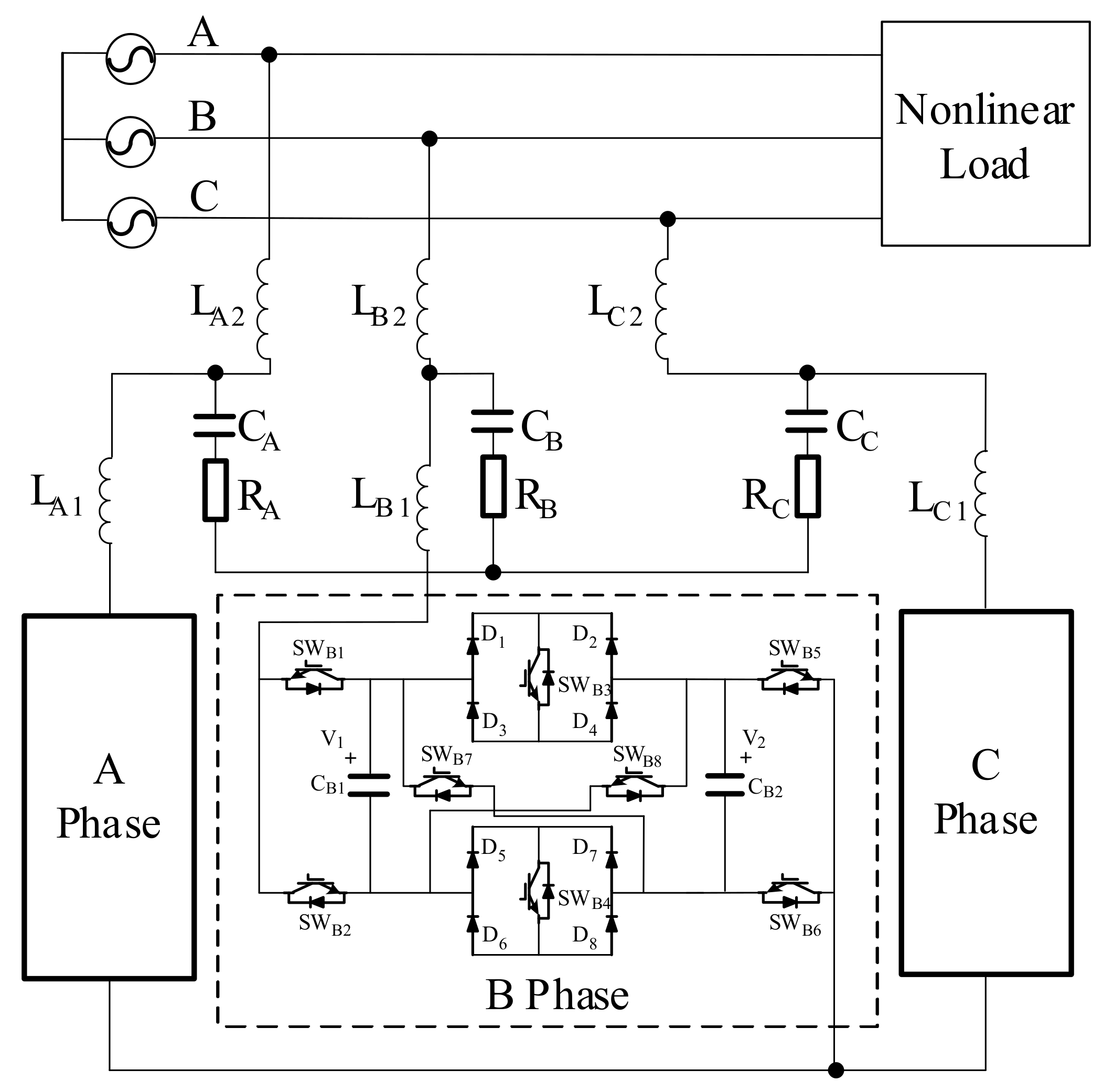
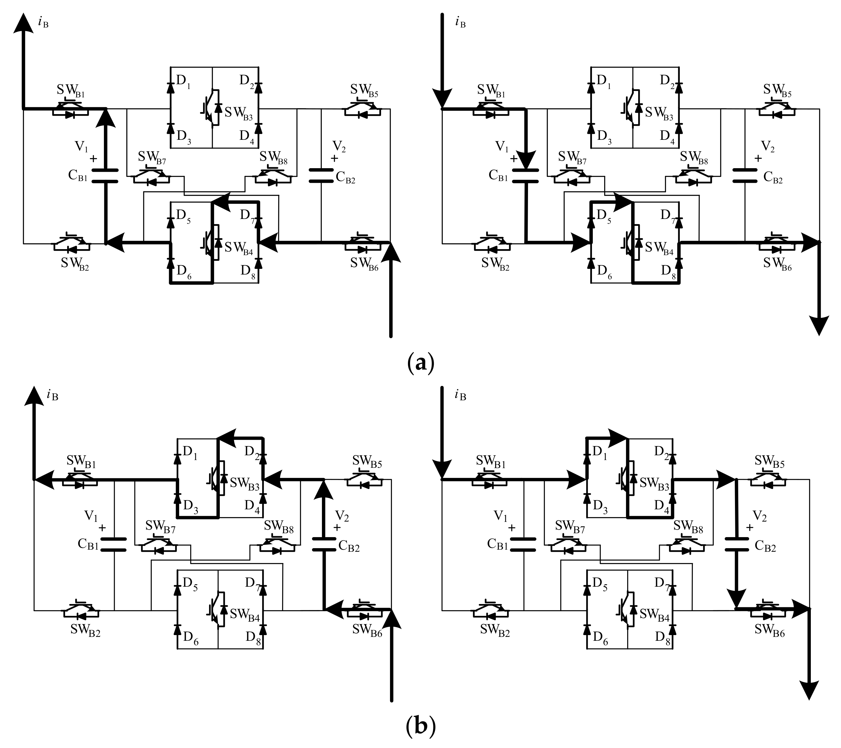
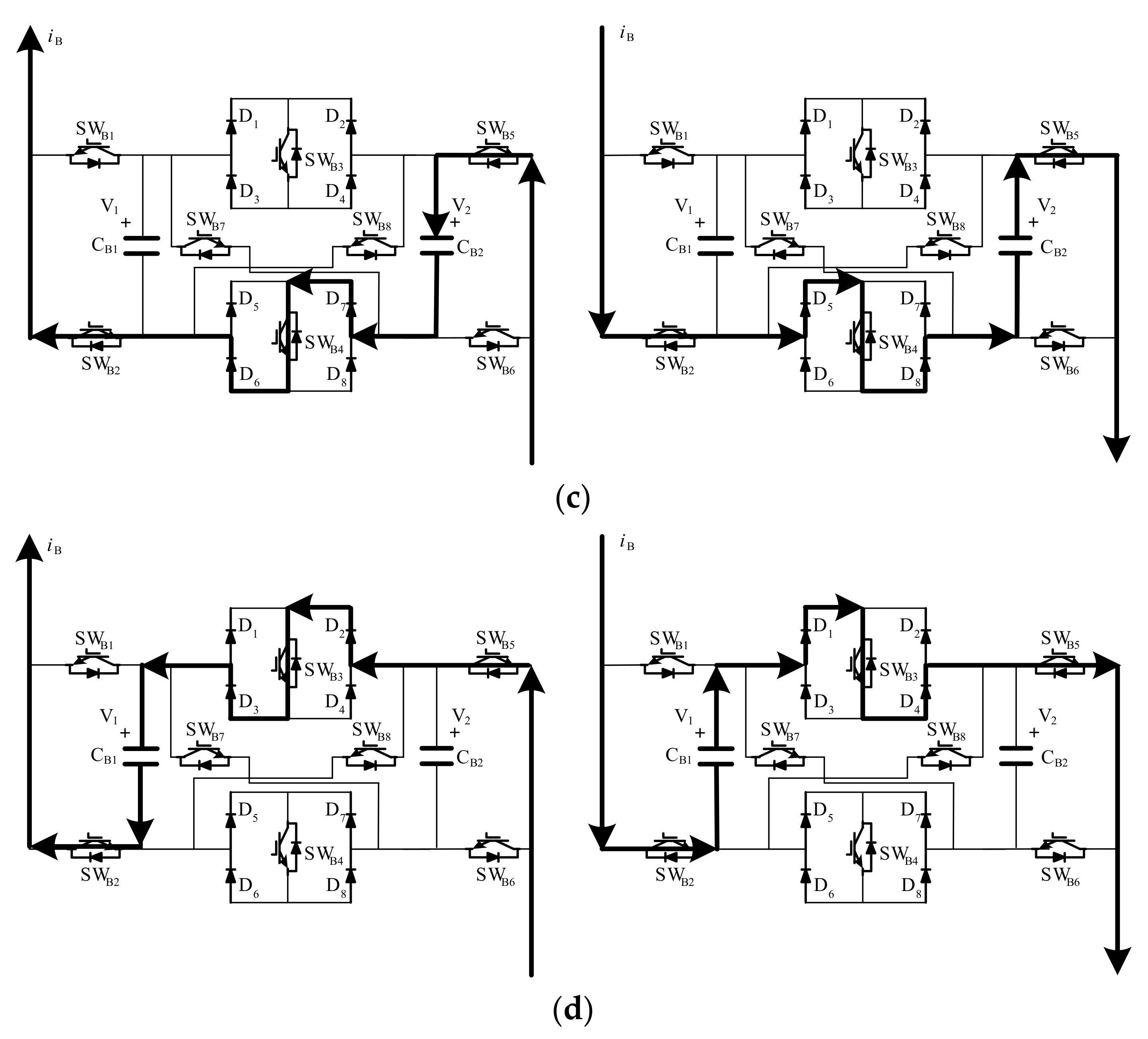
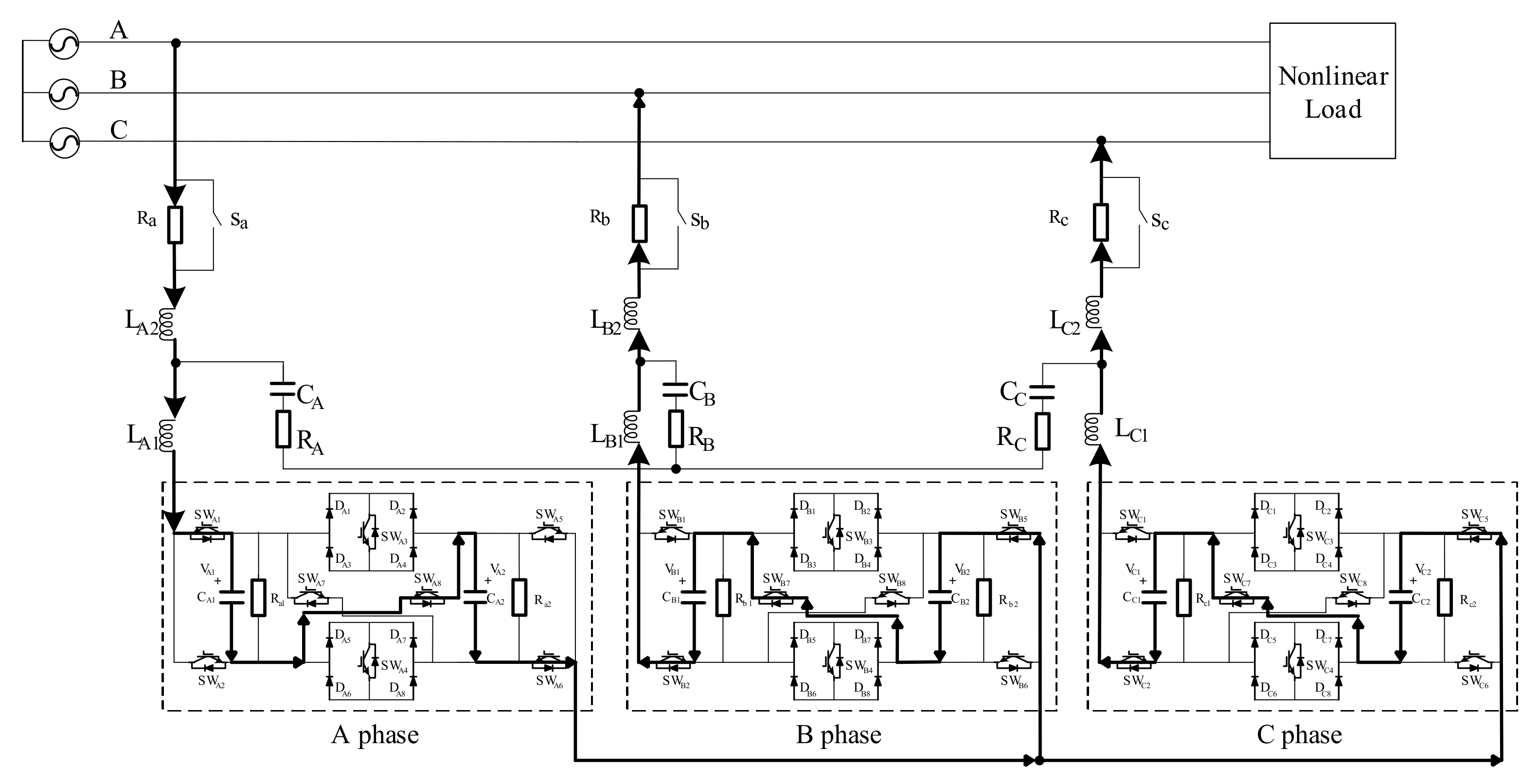
2.1. Presentation of the Novel Nine-Level Topology and Analysis of Its Working Mechanism
2.2. Comparison of Nine-Level Topology and Capacitance Voltage Control Strategy
2.2.1. Comparison of Nine-Level Topology
2.2.2. Comparison of Capacitance Voltage Control Strategy
3. Control Method of the APF System with the Novel Topology
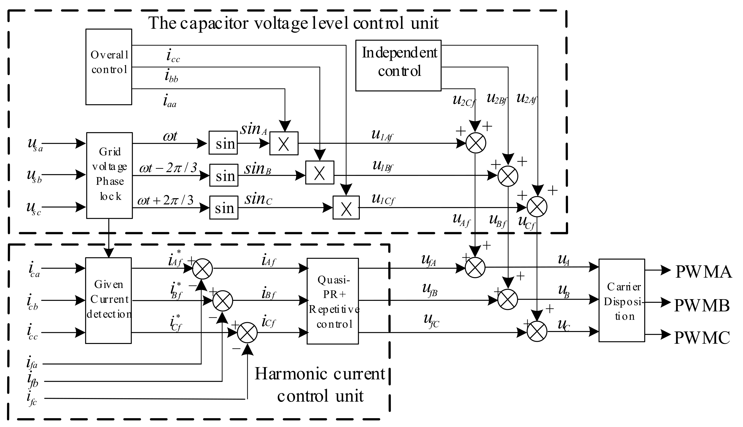
3.1. Overall Control Strategy of the System
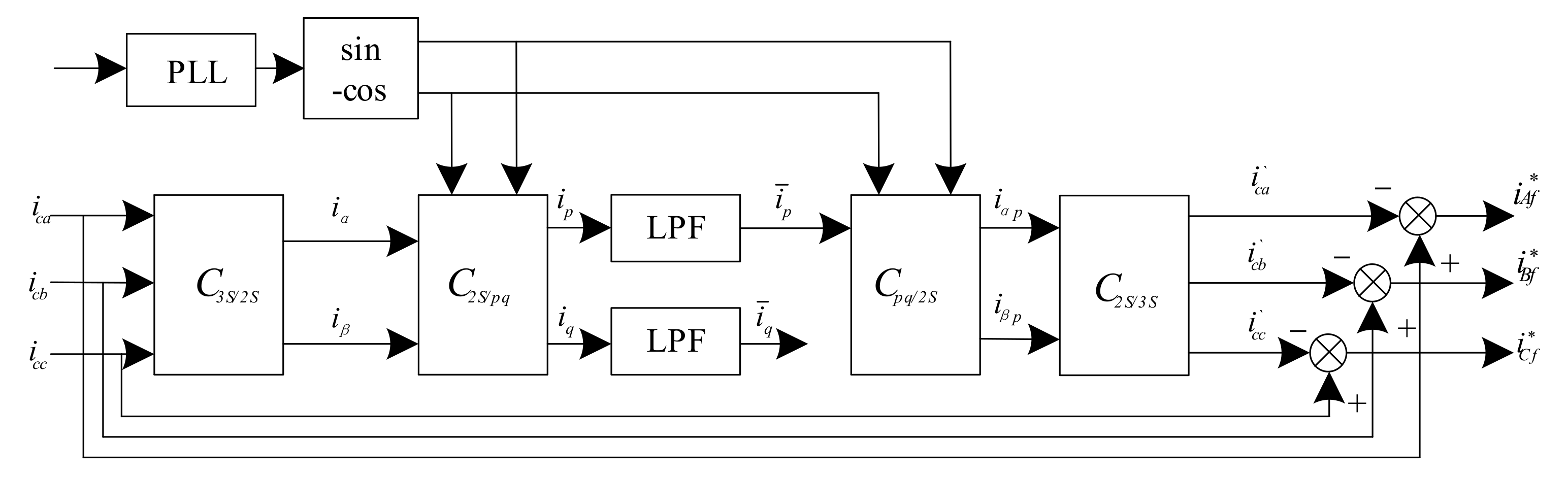
3.1.1. The Reference Current Detection Unit
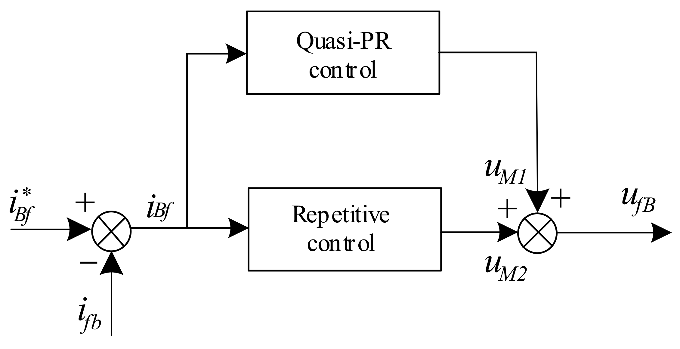
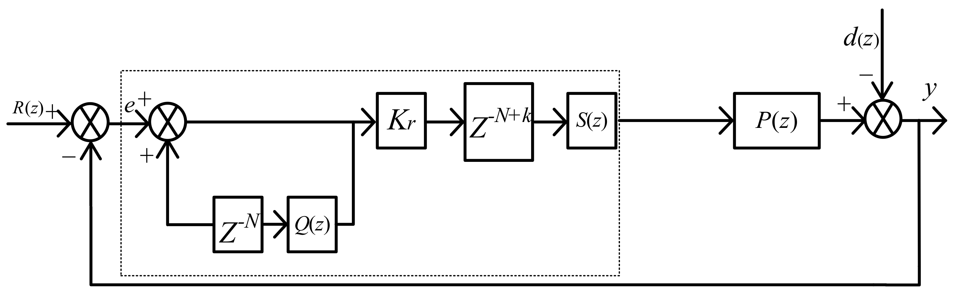
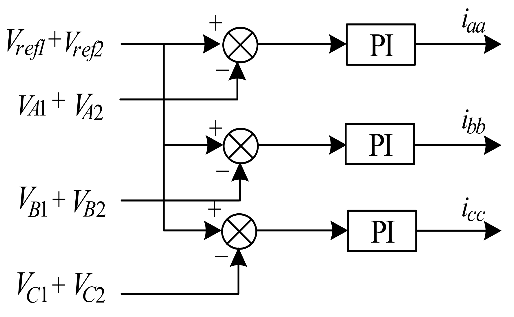
3.1.2. The Current Tracking Unit
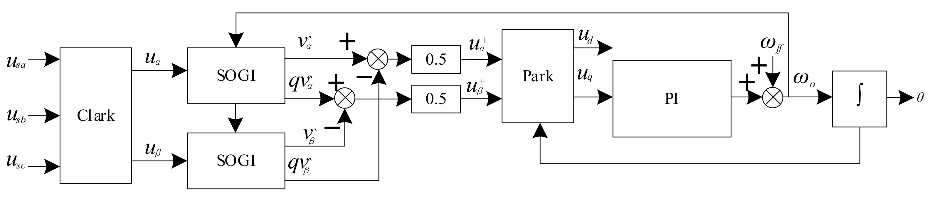
3.1.3. The Grid Voltage Phase-Locked Unit
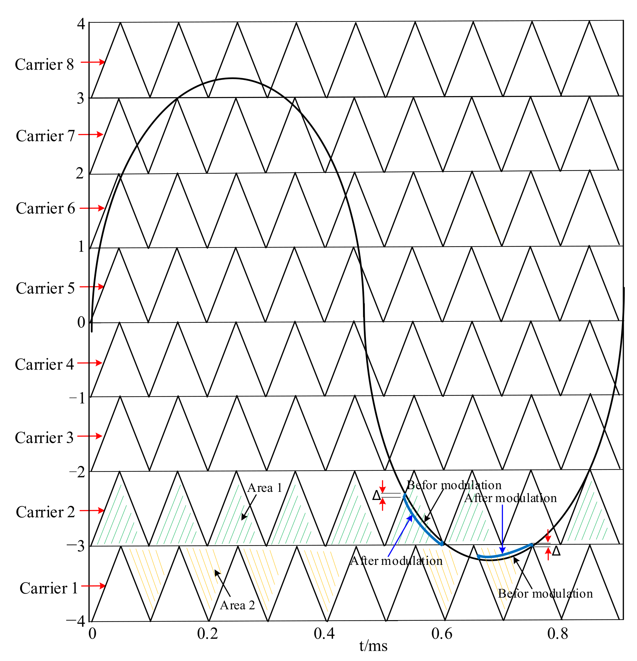
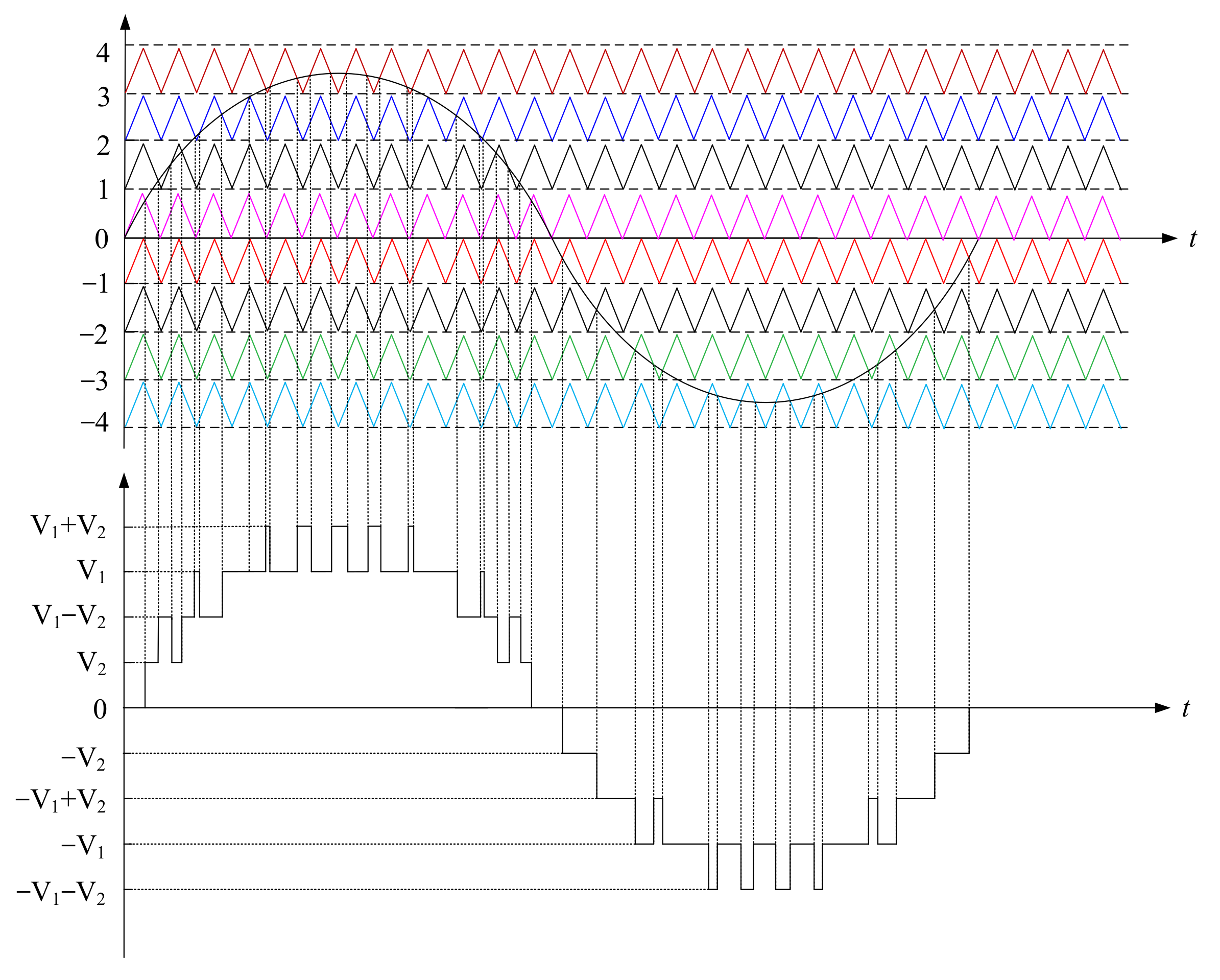
3.1.4. The Carrier Disposition Unit
3.2. Integrated Control Strategy of Phase Voltage
3.3. Control Strategy of the Cell Capacitance Voltage
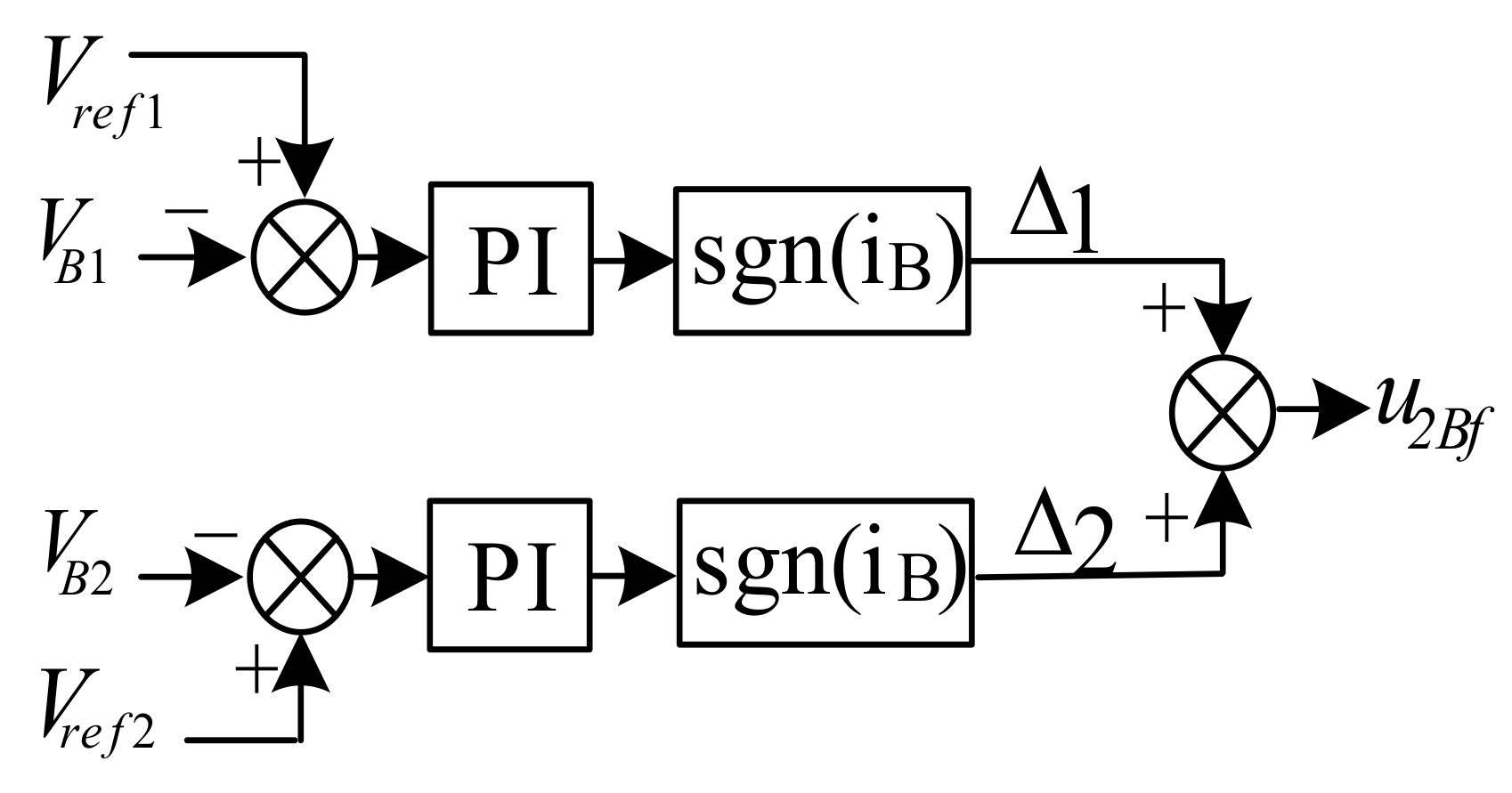
3.3.1. Determination of the Charge-Discharge State
3.3.2. Control Strategy of the Capacitor Voltage Regulation
3.4. Parameter Selection of the Passive Device
3.4.1. Parameter Selection of LCL
- Inductance parameter selection: It is assumed that the inductance relationship between the grid side and the inverter side is as follows:
- 2.
- Selection of capacitance parameters: The principle of capacitance selection is that the value of capacitance should be selected as small as possible to ensure that its impact can be completely ignored. The capacitance should be selected according to the rated power of APF. Generally, 5% of the rated power of APF is considered to be the threshold value of reactive power caused by the filter capacitor, and it is only necessary not to exceed the threshold value.
- 3.
- Resistance selection: The selection of resistance has a great influence on the system. If the selected value is too small, the resonance cannot be suppressed and large loss will be produced. If the resistance is selected too large, the suppression ability of LCL to high frequency harmonic will be reduced. The resistance is generally taken as 0.3 to 0.4 times of the capacitance impedance at resonance frequency,
3.4.2. Selection Guideline of the Capacitor
4. Simulation Study
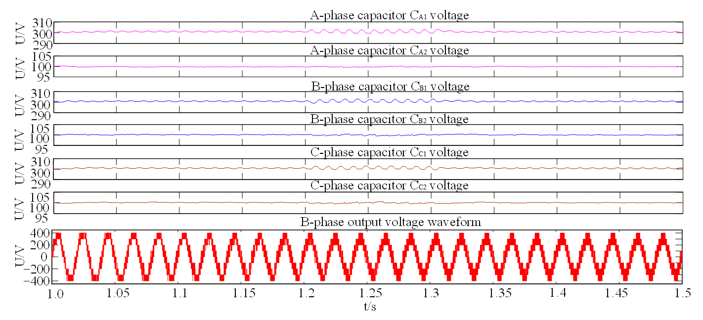
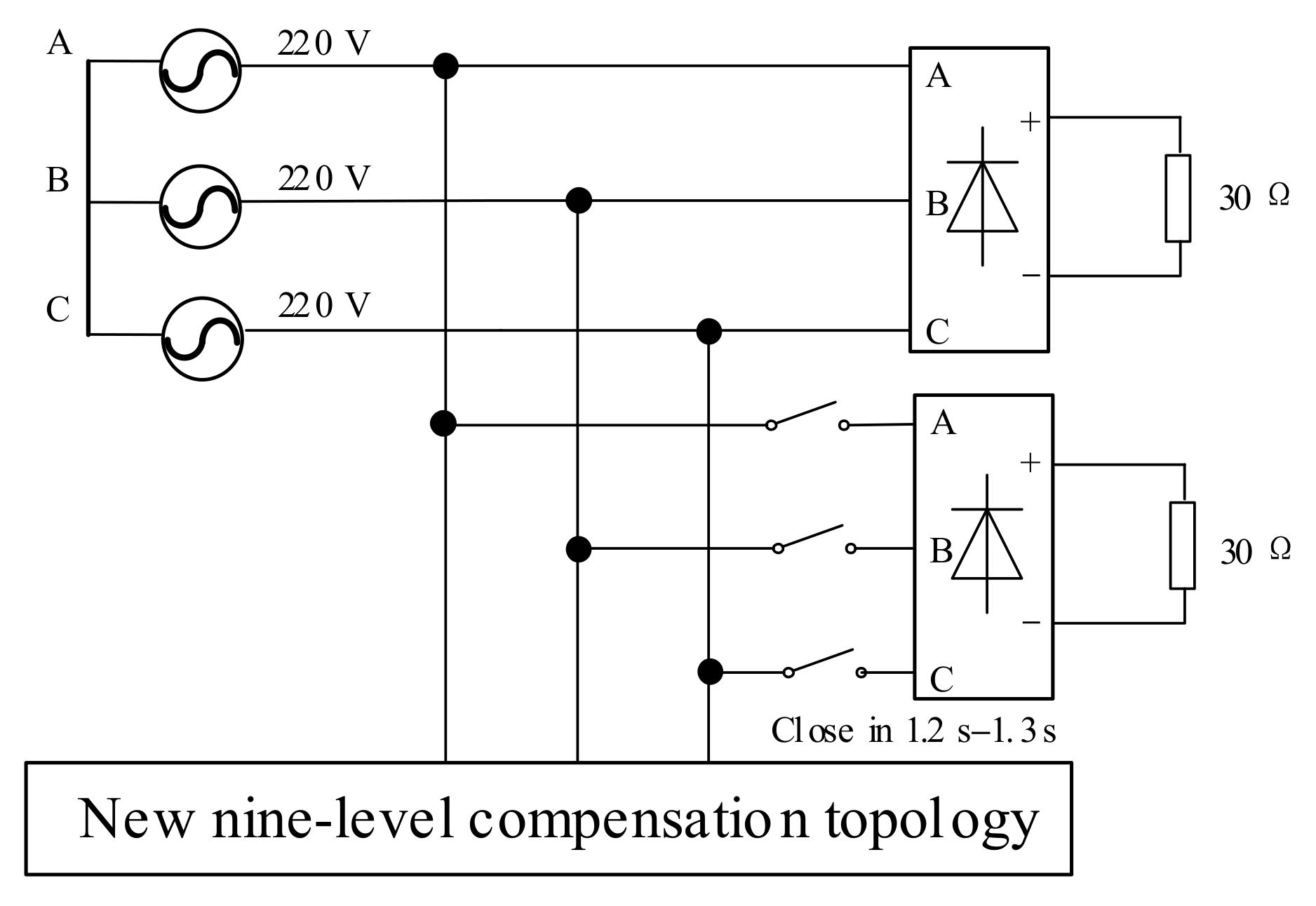
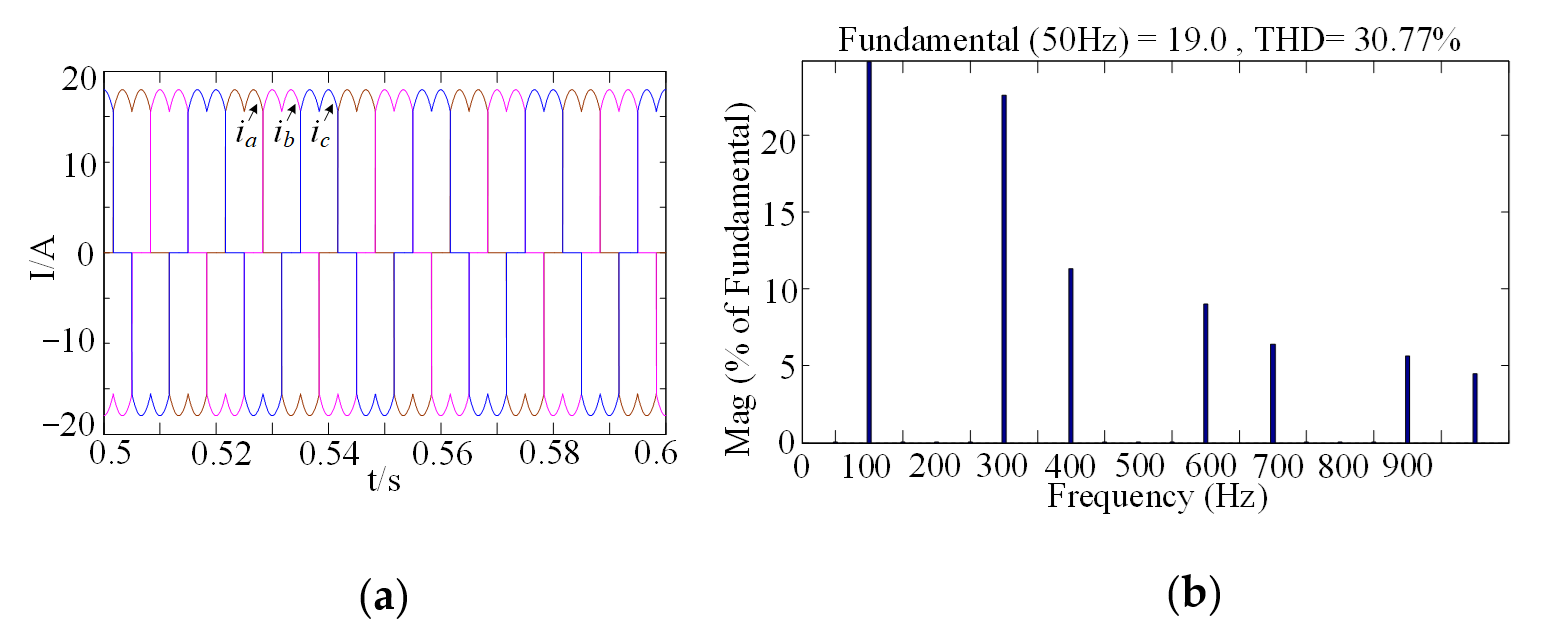
4.1. Balanced Load and Power Grid
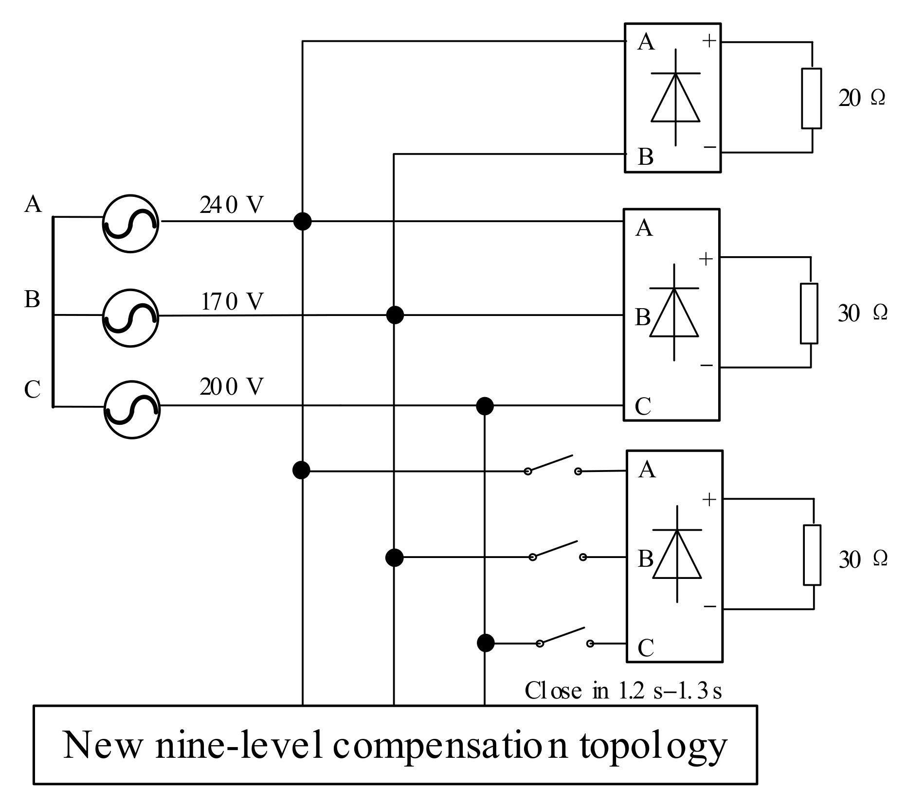
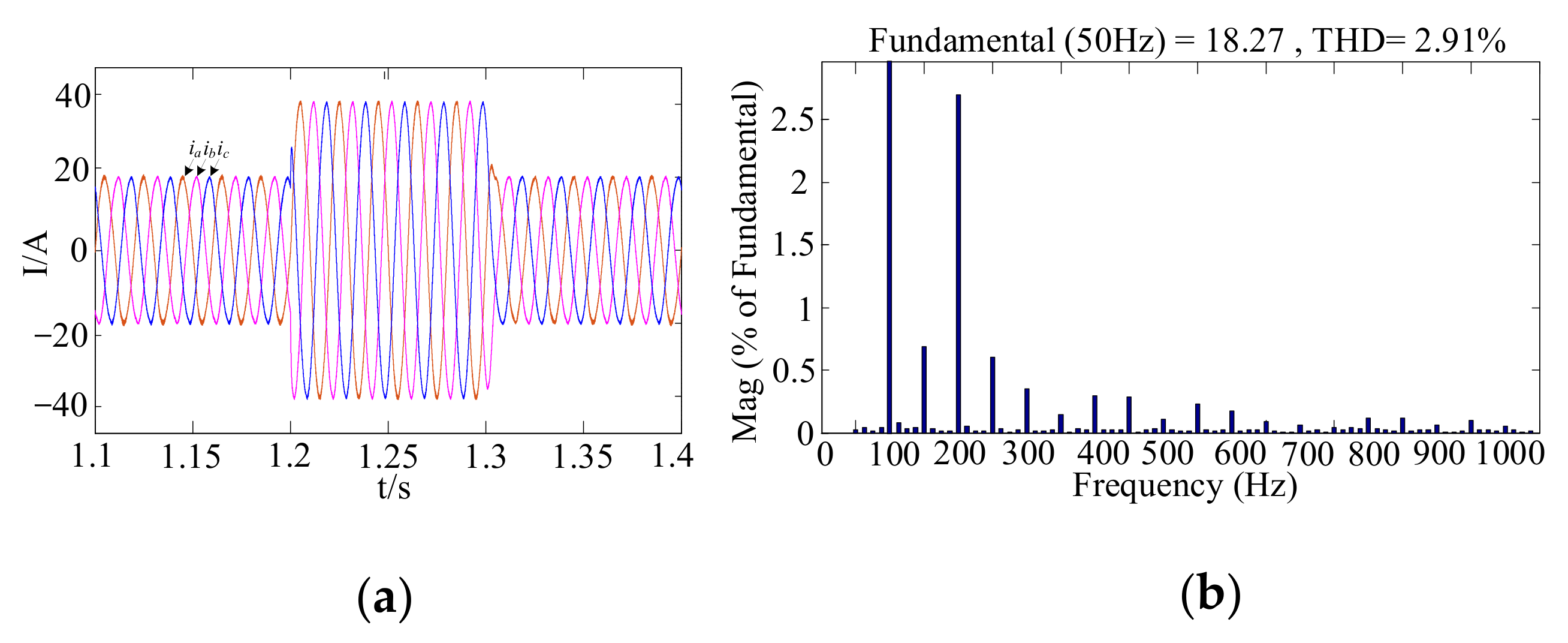
4.2. Unbalanced Load and Power Grid
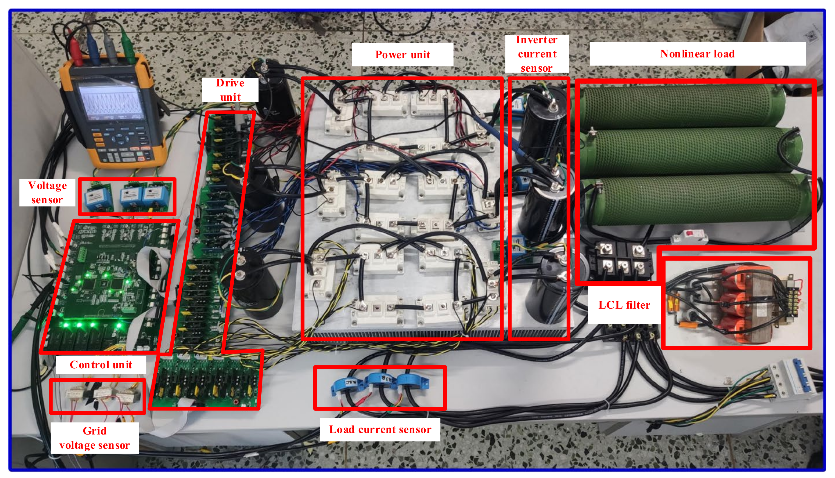
5. Experimental Section
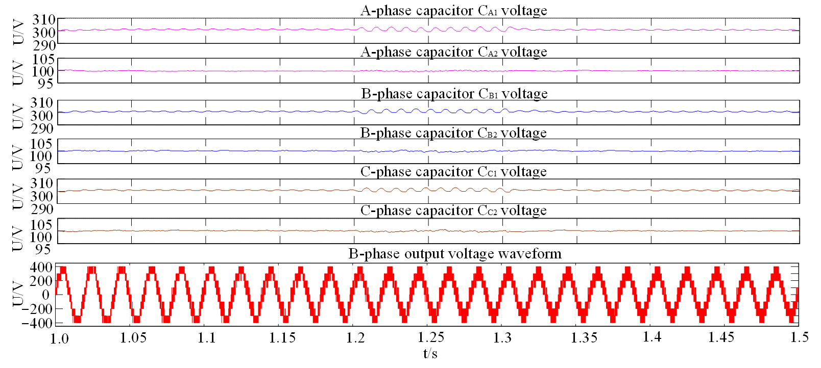
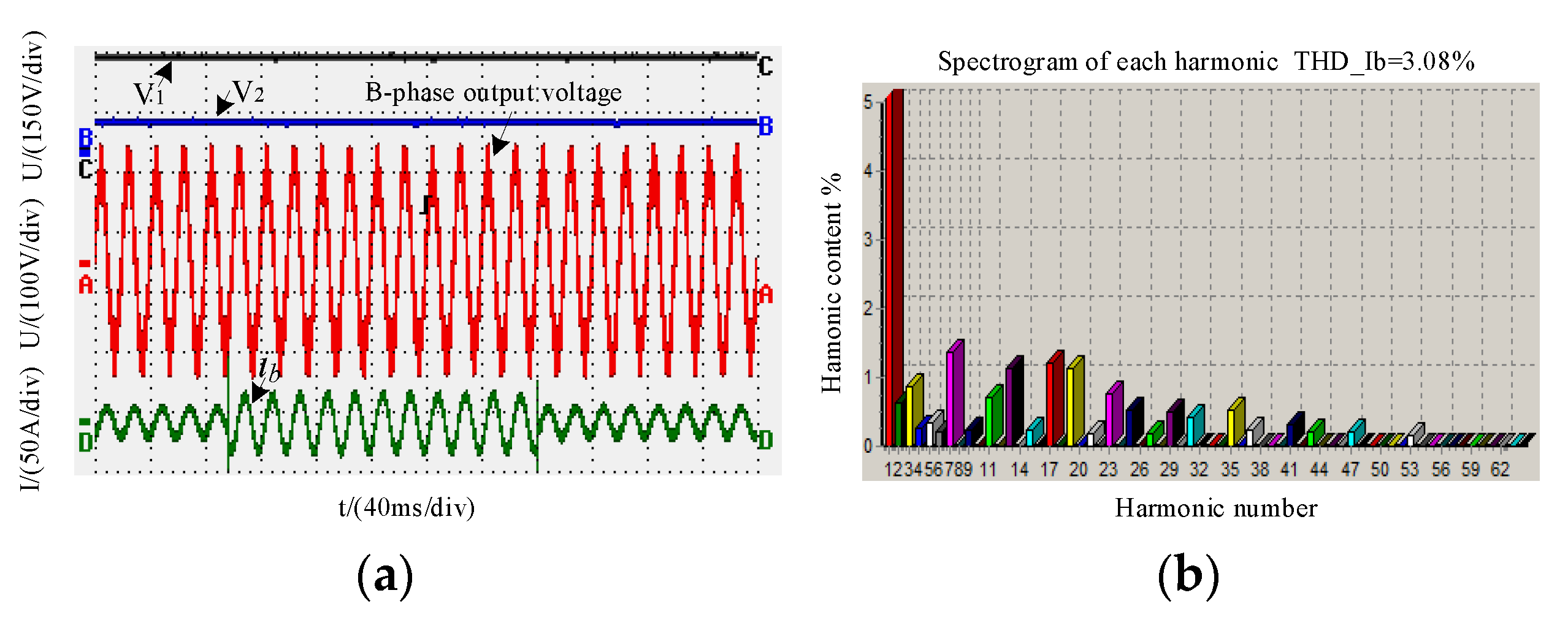
5.1. Balanced Load and Power Grid
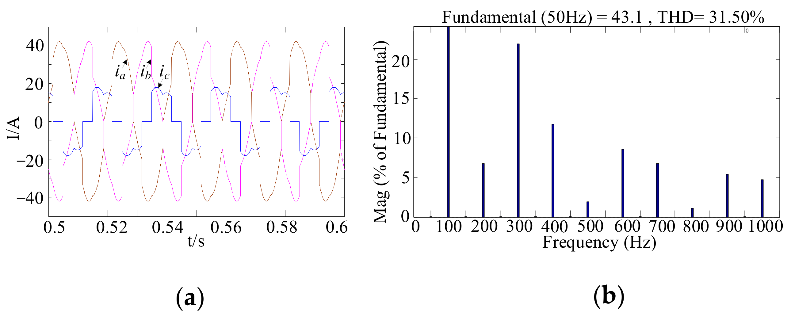
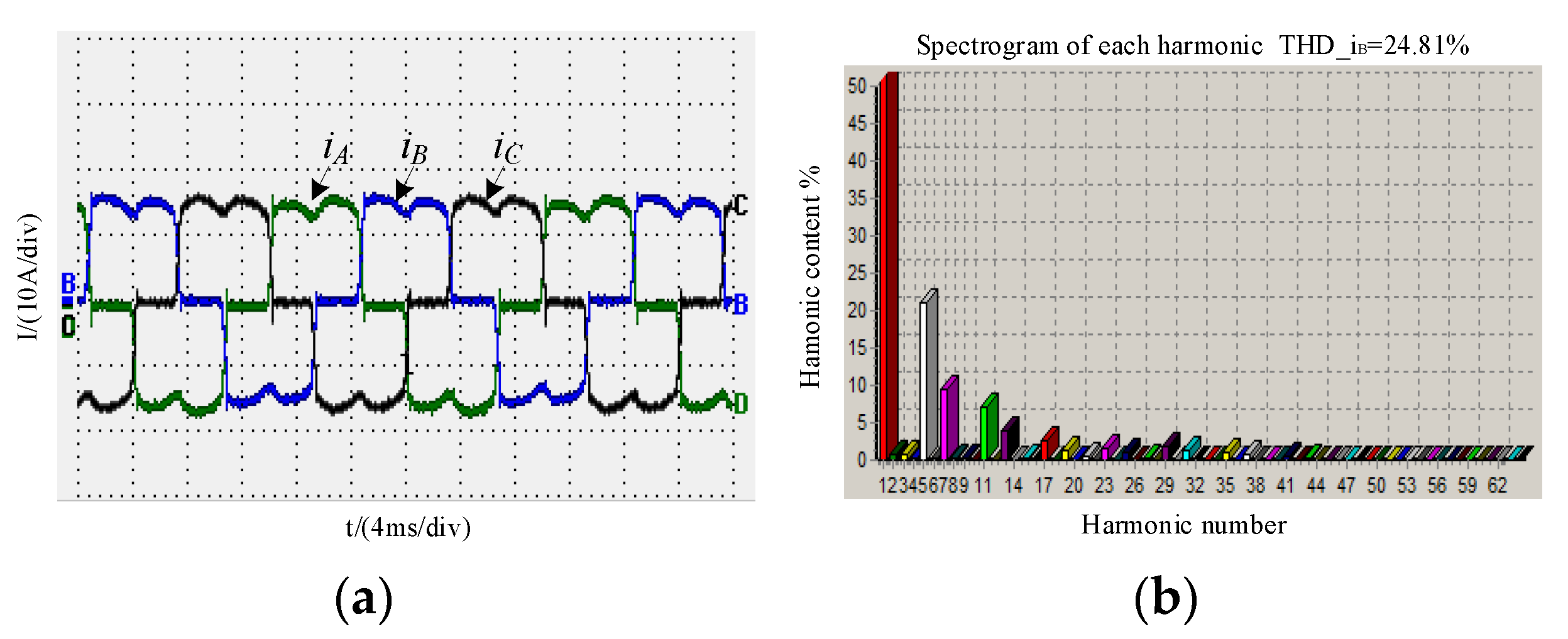
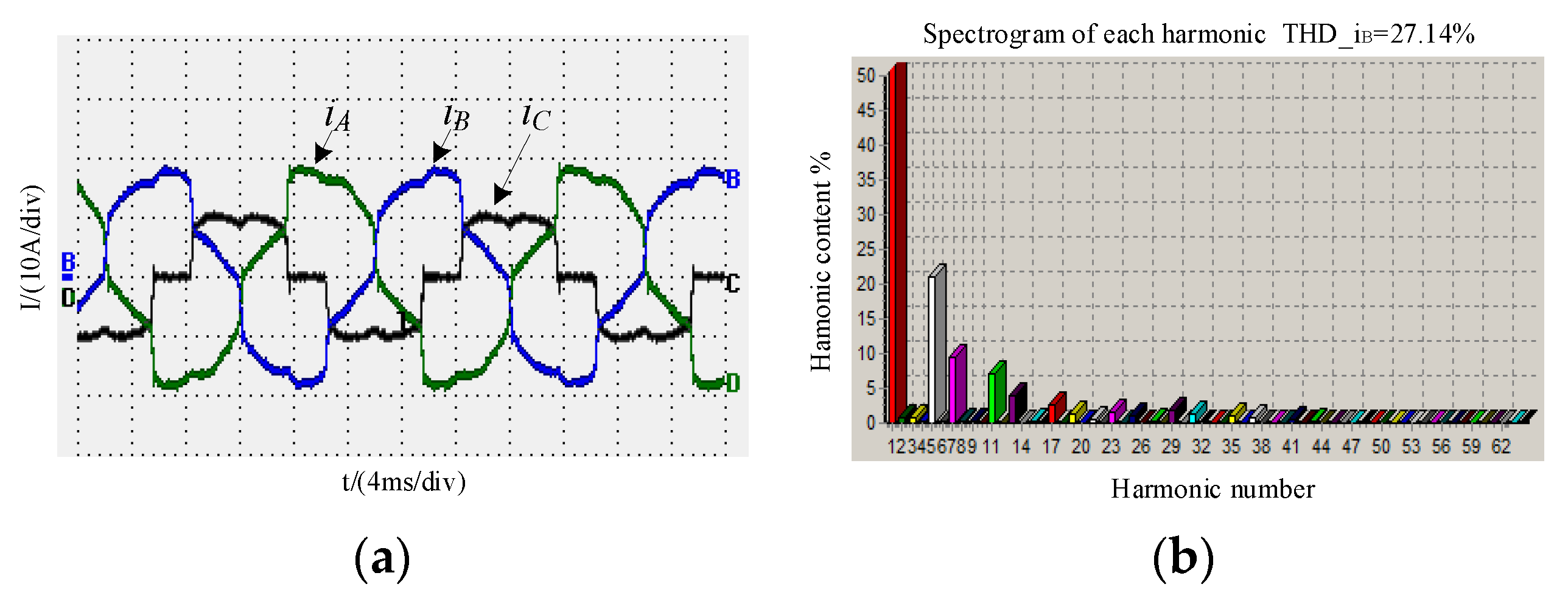
5.2. Unbalanced Load and Power Grid
6. Discussion
7. Conclusions and Future Work
Author Contributions
Funding
Data Availability Statement
Conflicts of Interest
References
- Yu, K.; Yang, Z.; Li, Y.; Yi, H.; Wang, F.; Zhuo, F. Three-phase three-level shunt APF control system based on multi-task parallel MCU. In Proceedings of the 2020 IEEE Applied Power Electronics Conference and Exposition (APEC), New Orleans, LA, USA, 15–19 March 2020; pp. 2392–2396. [Google Scholar]
- Bett, N.K.; Maina, C.C.; Hinga, P.K. New approach for design of shunt active power filter for power quality improvement in a three phase three wire system. In Proceedings of the 2020 IEEE PES/IAS Power Africa, Nairobi, Kenya, 25–28 August 2020; pp. 1–4. [Google Scholar]
- Büyük, M.; Tan, A.; Bayindir, K.C.; Tümay, M. Analysis and comparison of passive damping methods for shunt active power filter with output LCL filter. In Proceedings of the 2015 Intl Aegean Conference on Electrical Machines & Power Electronics (ACEMP), 2015 Intl Conference on Optimization of Electrical & Electronic Equipment (OPTIM) & 2015 Intl Symposium on Advanced Electromechanical Motion Systems (ELECTROMOTION), Side, Turkey, 2–4 September 2015; pp. 434–440. [Google Scholar]
- Zhang, G.P.; Zhou, Y.S.; Zheng, Z.; Wang, X.H. Research on current-limiting optimization strategy for specific harmonic compensation of active power filter. Power Syst. Prot. Control 2018, 46, 46–53. [Google Scholar]
- Alishah, R.S.; Hosseini, S.; Babaei, H.E.; Sabahi, M. Optimal design of new cascaded switch-ladder multilevel inverter structure. IEEE Trans. Ind. Electron. 2017, 64, 2072. [Google Scholar] [CrossRef]
- Prasetiyo, N.N.; Pratomo, L.H. Design and implementation of inverter single phase nine-level using PIC18F4550. In Proceedings of the 2018 5th International Conference on Information Technology, Computer, and Electrical Engineering (ICITACEE), Semarang, Indonesia, 27–28 September 2018; pp. 84–88. [Google Scholar]
- Kumar, G.; Equbal, M.D.; Ghosh, R. Control strategy of diode clamped multilevel inverter with pv system as separate dc source. In Proceedings of the 2019 International Conference on Power Electronics, Control and Automation (ICPECA), New Delhi, India, 16–17 November 2019; pp. 1–5. [Google Scholar]
- Singhai, S.; Pandey, A.; Singh, V. New topology of asymmtrical multilevel inverter [15/29 Level]. In Proceedings of the 2018 International Conference on Current Trends towards Converging Technologies (ICCTCT), Coimbatore, India, 1–3 March 2018; pp. 1–6. [Google Scholar]
- Koshti, K.; Rao, M.N. A brief review on multilevel inverter topologies. In Proceedings of the 2017 International Conference on Data Management Analytics and Innovation (ICDMAI), Pune, India, 24–26 February 2017; pp. 187–193. [Google Scholar]
- Amamra, S.; Meghriche, K.; Cherifi, A.; Francois, B. Multilevel inverter topology for renewable energy grid integration. IEEE Trans. Ind. Electron. 2017, 64, 8855–8866. [Google Scholar] [CrossRef]
- Shi, S.; Wang, X.; Zheng, S.; Zhang, Y.; Lu, D. A new diode-clamped multilevel inverter with balance voltages of dc capacitors. IEEE Trans. Energy Convers. 2018, 33, 2220–2228. [Google Scholar] [CrossRef]
- Zolfaghar, M.; Najafi, E.; Hasanzadeh, S. A modified diode clamped inverter with reduced number of switches. In Proceedings of the 2018 9th Annual Power Electronics Drives Systems and Technologies Conference (PEDSTC), Tehran, Iran, 14–15 February 2018; pp. 53–58. [Google Scholar]
- Ahmed, B.; Aganah, K.A.; Ndoye, M.; Arif, M.A.; Luciano, C.; Murphy, G.V. Single-phase cascaded multilevel inverter topology for distributed DC sources. In Proceedings of the 2017 IEEE 8th Annual Ubiquitous Computing, Electronics and Mobile Communication Conference (UEMCON), New York, NY, USA, 19–21 October 2017; pp. 514–519. [Google Scholar]
- Shahina, E.P.; Aravind, K.; Jarin, T. THD reduction in execution of a nine level single phase inverter. In Proceedings of the 2020 International Conference on Communication and Signal Processing (ICCSP), Chennai, India, 28–30 July 2020; pp. 1185–1189. [Google Scholar]
- Veenstra, M.; Rufer, A. Control of a hybrid asymmetric multilevel inverter for competitive medium-voltage industrial drives. IEEE Trans. Ind. Appl. 2005, 41, 655–664. [Google Scholar] [CrossRef]
- Gao, H.; Zhang, P.; Liu, X.; Feng, S.; Ma, J.; Li, R. Seven-level active power filter based on a novel h-bridge power topology structure. Energies 2019, 12, 2997. [Google Scholar] [CrossRef] [Green Version]
- Amini, J.; Moallem, M. DC link capacitor voltage balancing method for diode-clamped multilevel converters. In Proceedings of the 2019 IEEE 28th International Symposium on Industrial Electronics (ISIE), Vancouver, BC, Canada, 12–14 June 2019; pp. 793–797. [Google Scholar]
- Xu, C.; Dai, K.; Kang, Y.; Liu, C. Characteristic analysis and experimental verification of a novel capacitor voltage control strategy for three-phase MMC-DSTATCOM. In Proceedings of the 2015 IEEE Applied Power Electronics Conference and Exposition (APEC), Charlotte, NC, USA, 15–19 March 2015; pp. 1528–1533. [Google Scholar]
- Angulo, M.; Lezana, P.; Kouro, S.; Rodriguez, J.; Wu, B. Level-shifted PWM for cascaded multilevel inverters with even power distribution. In Proceedings of the 2007 IEEE Power Electronics Specialists Conference, Orlando, FL, USA, 17–21 June 2007; pp. 2373–2378. [Google Scholar]
- Sochor, P.; Akagi, H. Theoretical and experimental comparison between phase-shifted PWM and level-shifted PWM in a modular multilevel SDBC inverter for utility-scale photovoltaic applications. IEEE Trans. Ind. Appl. 2017, 53, 4695–4707. [Google Scholar] [CrossRef]
- Sandeep, N.; Yaragatti, U.R. Operation and control of a nine-level modified anpc inverter topology with reduced part count for grid-connected applications. IEEE Trans. Ind. Electron. 2018, 65, 4810–4818. [Google Scholar] [CrossRef]
- Karimi, M.; Kargar, P.; Varesi, K. Two novel switched-capacitor based multi-level inverter topologies. In Proceedings of the 2019 International Power System Conference (PSC), Tehran, Iran, 9–11 December 2019; pp. 391–396. [Google Scholar]
- Tarvirdiln-Asl, R.; Narimani, M. A new nine-level voltage source inverter with capacitor voltage balancing. In Proceedings of the IECON 2018 44th Annual Conference of the IEEE Industrial Electronics Society, Washington, DC, USA, 21–23 October 2018; pp. 907–912. [Google Scholar]
- Mohamed, B.H.; Mekhilef, S. Digital predictive current control of multilevel four-leg voltage source inverter under balanced and unbalanced load conditions. IET Electr. Power Appl. 2017, 11, 1499–1508. [Google Scholar]
- Janpong, S.; Narongrit, T.; Puangpool, M.; Suthikarnnarunai, N. DC-bus voltage control for single-phase active power filter using neural network. In Proceedings of the 2019 International Conference on Power, Energy and Innovations (ICPEI), Pattaya, Thailand, 16–18 October 2019; pp. 60–63. [Google Scholar]


| SW Status | Output State | |||||||
|---|---|---|---|---|---|---|---|---|
| SWB1 | SWB2 | SWB3 | SWB4 | SWB5 | SWB6 | SWB7 | SWB8 | |
| 1 | 0 | 0 | 0 | 0 | 1 | 0 | 1 | V1 + V2 = 4V2 |
| 1 | 0 | 0 | 1 | 0 | 1 | 0 | 0 | +V1 = 3V2 |
| 1 | 0 | 0 | 1 | 1 | 0 | 0 | 0 | V1 − V2 = 2V2 |
| 1 | 0 | 1 | 0 | 0 | 1 | 0 | 0 | +V2 |
| 1 | 0 | 1 | 0 | 1 | 0 | 0 | 0 | 0 |
| 0 | 1 | 0 | 1 | 1 | 0 | 0 | 0 | −V2 |
| 0 | 1 | 1 | 0 | 0 | 1 | 0 | 0 | −(V1 − V2) = −2V2 |
| 0 | 1 | 1 | 0 | 1 | 0 | 0 | 0 | −V1 = −3V2 |
| 0 | 1 | 0 | 0 | 1 | 0 | 1 | 0 | −(V1 + V2) = −4V2 |
| Structure | New Topology | Cascade H-Bridge Nine-Level | [21] | [22] | |
|---|---|---|---|---|---|
| Category | |||||
| Topology |  |  | 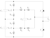 |  | |
| Number of power switches | 8 | 16 | 10 | 9 | |
| Number of capacitors | 2 | 4 | 3 | 2 | |
| Current | iB > 0 | iB < 0 | |
|---|---|---|---|
| Output Level | |||
| 9: V1 + V2 = 4V2 | - | - | |
| 8: V1 = 3V2 | CB1 discharge, CB2 suspend | CB1 charge, CB2 suspend | |
| 7: V1 − V2 = 2V2 | - | - | |
| 6: V2 | CB2 discharge, CB1 suspend | CB2 charge, CB1 suspend | |
| 5: 0 | - | - | |
| 4: −V2 | CB2 charge, CB1 suspend | CB2 discharge, CB1 suspend | |
| 3: −(V1 − V2) = −2V2 | - | - | |
| 2: −V1 = −3V2 | CB1 charge, CB2 suspend | CB1 discharge, CB2 suspend | |
| 1: −(V1 + V2) = −4V2 | - | - | |
| Carrier | 8 | 7 | 6 | 5 | 4 | 3 | 2 | 1 | |
|---|---|---|---|---|---|---|---|---|---|
| Output Level | State | Up (↑) or Down (↓) | |||||||
| 8: V1 = 3V2 | discharge | ↓ | ↑ | - | - | - | - | - | - |
| charge | ↑ | ↓ | - | - | - | - | - | - | |
| 6: V2 | discharge | - | - | ↓ | ↑ | - | - | - | - |
| charge | - | - | ↑ | ↓ | - | - | - | - | |
| 4: −V2 | discharge | - | - | - | - | ↓ | ↑ | - | - |
| charge | - | - | - | - | ↑ | ↓ | - | - | |
| 2: −V1 = −3V2 | discharge | - | - | - | - | - | - | ↓ | ↑ |
| charge | - | - | - | - | - | - | ↑ | ↓ | |
| Parameters | Value |
|---|---|
| The voltage V1 | 300 V |
| The voltage V2 | 100 V |
| The capacitor C1, C2 | 1000 µF |
| The inductor L1, L2 | 2 mH, 1 mH |
| Three-phase balanced grid voltage | 220 V, 220 V, 220 V |
| The balanced load R | 30 Ω |
| Three-phase unbalanced grid voltage | 240 V, 170 V, 200 V |
| Rectifier load RAB | 20 Ω |
Publisher’s Note: MDPI stays neutral with regard to jurisdictional claims in published maps and institutional affiliations. |
© 2021 by the authors. Licensee MDPI, Basel, Switzerland. This article is an open access article distributed under the terms and conditions of the Creative Commons Attribution (CC BY) license (https://creativecommons.org/licenses/by/4.0/).
Share and Cite
Gao, H.; Liu, X.; Ren, M.; Feng, S.; Li, Z. A Novel Multilevel Controller. Electronics 2021, 10, 1222. https://doi.org/10.3390/electronics10101222
Gao H, Liu X, Ren M, Feng S, Li Z. A Novel Multilevel Controller. Electronics. 2021; 10(10):1222. https://doi.org/10.3390/electronics10101222
Chicago/Turabian StyleGao, Hanying, Xiangnan Liu, Mingjie Ren, Shuai Feng, and Zhiying Li. 2021. "A Novel Multilevel Controller" Electronics 10, no. 10: 1222. https://doi.org/10.3390/electronics10101222
APA StyleGao, H., Liu, X., Ren, M., Feng, S., & Li, Z. (2021). A Novel Multilevel Controller. Electronics, 10(10), 1222. https://doi.org/10.3390/electronics10101222