1. Introduction
In the last two decades, there has been an increase in research aimed at different techniques for harvesting energy from the environment, and in particular, those associated with radio frequency (RF) signals known as RF energy harvesting (RF-EH), wireless energy harvesting (WEH) or RF energy harvesting wireless communication (RF-EHWC) [
1,
2,
3]. One of the main objectives of such techniques is to use available energy from the environment to be used to support the node power schemes for wireless sensor networks (WSN) and Internet of things (IoT) systems [
3,
4]. Thus, it is desired to keep the devices running without the use of batteries. The IoT schemes have seen significant research intending to make them more energy-efficient, secure, and affordable. Thus, the concept of green information and communication technology focuses on green RF identification (RFID) technology, green sensor networks technology, green cellular networks, etc. IoT poses a high potential to bolster environmental sustainability and economic with the advancements of enabling technologies [
5].
Dedicated sensors can be deployed in selected areas for data gathering and measuring global and local desired variables. A sensor node contains several small, low-cost, and low-power electronic devices such as a sensing unit, a storage unit, a processing unit, and a communication unit [
5]. However, the footprint and power autonomy for such sensors usually are scarce. However, the sensors still need modules that allow them the sharing of information and the requirement to protect the information that they are sharing, for example, in a wireless sensor network (WSN) [
5,
6]. A tendency is to move the complexity and power demand of dedicated communication units to central entities such base stations or even employ mobile agents to visit the IoT sensors using UAVs to assuage the requirements for power operations [
5]. However, the nodes need to have embedded structures to protect the data since electronic attacks are unavoidable. Device-to-device (D2D) protocols can be adopted in the sensor due to the reduced resources required for its implementation [
6].
Thus, the extraction and efficient use of energy to run all the processes involved in an IoT becomes very important. In this regard, some of the works have focused on using energy from RF signals such as radio, television, cellular phones, and WiFi due to the massification of these technologies [
7,
8]. Among the investigations carried out, there are examples of systems that even make simultaneous use of several frequency bands [
9,
10,
11,
12] to take advantage of a greater spectrum which is reflected in greater energy collected.
Similarly, there are works aimed at energy harvesting in indoor and outdoor environments [
7,
13,
14,
15] where outdoor solutions are generally applied to permanent carrier signals, constant power, or transmission systems of the metropolitan area. In contrast, for indoors, short-range systems and dynamic carrier power are used. This parameter presents the most significant challenges from the design side. Some of the challenges presented in this scenario are low energy levels in the environment, power dependency on the use of the network, and non-linearity in the reception module of a harvester.
It is necessary to consider the different parameters of the target signal to develop an energy harvesting system with RF signals, such as modulation, frequency, and power transmission. In particular, for WiFi, signal emission regulations limit the power transmission from a common access point (AP) or router to 20 dBm maximum, requiring the use of multiple schemes to take advantage of these reduced levels present in the environment [
16]. Besides, evaluating the WiFi signal transmission form establishes strategies that allow better use of the available energy.
Thus, Reference [
17] presents the design, development, and evaluation of a rectifier circuit prototype to apply the energy collection of 2.45 GHz signals, obtaining an RF/DC conversion efficiency of 68% at −10 dBm in simulation and 33% to −5 dBm of the built prototype. Reference [
18] presents the design of an RF energy harvesting system based on three harvesters using three-panel antennas to cover three channels of the 2.4 GHz WiFi band. The output of the three blocks is connected to a voltage multiplier circuit. It uses a supercapacitor as a storage medium, collecting 0.45 V in 6 to 7 h, and then going to a second conversion stage increases the output to 2 V. The work concludes that the proposed system can supply power to electronic devices with a power consumption of less than 1 mW. In [
13], the design of a WiFi energy collector for indoor use is described, which operates at low incident power and conversion efficiency of 61%, managing to collect 1.67 mJ of energy in an operation of 38 h on a 1 mF supercapacitor with a voltage of 1.8 V.
In [
19], a collector is developed to feed a temperature sensor node and a camera at 5 m and 6 m, respectively; but requiring the modification of the router so that it transmits between the silence spaces that occur due to the absence of network traffic, turning the router into a dedicated power generator.
From state of the art, it could be stated that WiFi energy harvesting systems are mainly focused on harvester development. From the authors knowledge, the works do not concentrate on the effects of this technology transmission method, which influences the collector performance and the amount of energy collected.
Thus, the purpose of this work is to consider both sides of the problem. On the one hand, the nature of the WiFi signal is considered to explore approaches to better utilize the energy available without requiring modifications on routers not considered as standard configurations and operation of this equipment. Hence, in particular, the use of routers or APs with multiple SSID is explored to increase the amount of energy harvested in low traffic conditions given the nature of the WiFi technology. On the other hand, the harvesting circuit is addressed to devise a system as simple as possible while maintaining adequate performance. Thus, the so-called rectenna design and the power management system are developed, emphasizing a simplistic architecture featuring low cost and low power consumption. Therefore, at the end, a working prototype is developed to work in an actual environment (houses and buildings) and showing the potential to deliver enough energy to operate electronic devices such as those employed for IoT-type systems even in cases of low-traffic condition on a WiFi network.
2. WiFi Transmission Signal Behavior
It is important to check the WiFi transmission signal behavior to design an energy harvester aimed properly. Thus, for a typical AP or router, the WiFi standard periodically sends a signal called beacon [
20], a packet containing router data information that allows the users to connect to it. This pilot signal can be configured to be sent from the router every 40 to 1000 ms, a time known as the beacon interval (BI). By default, the BI is configured to 100 ms. If there are no users connected to the router, the beacon signal becomes the only signal emitted by the equipment.
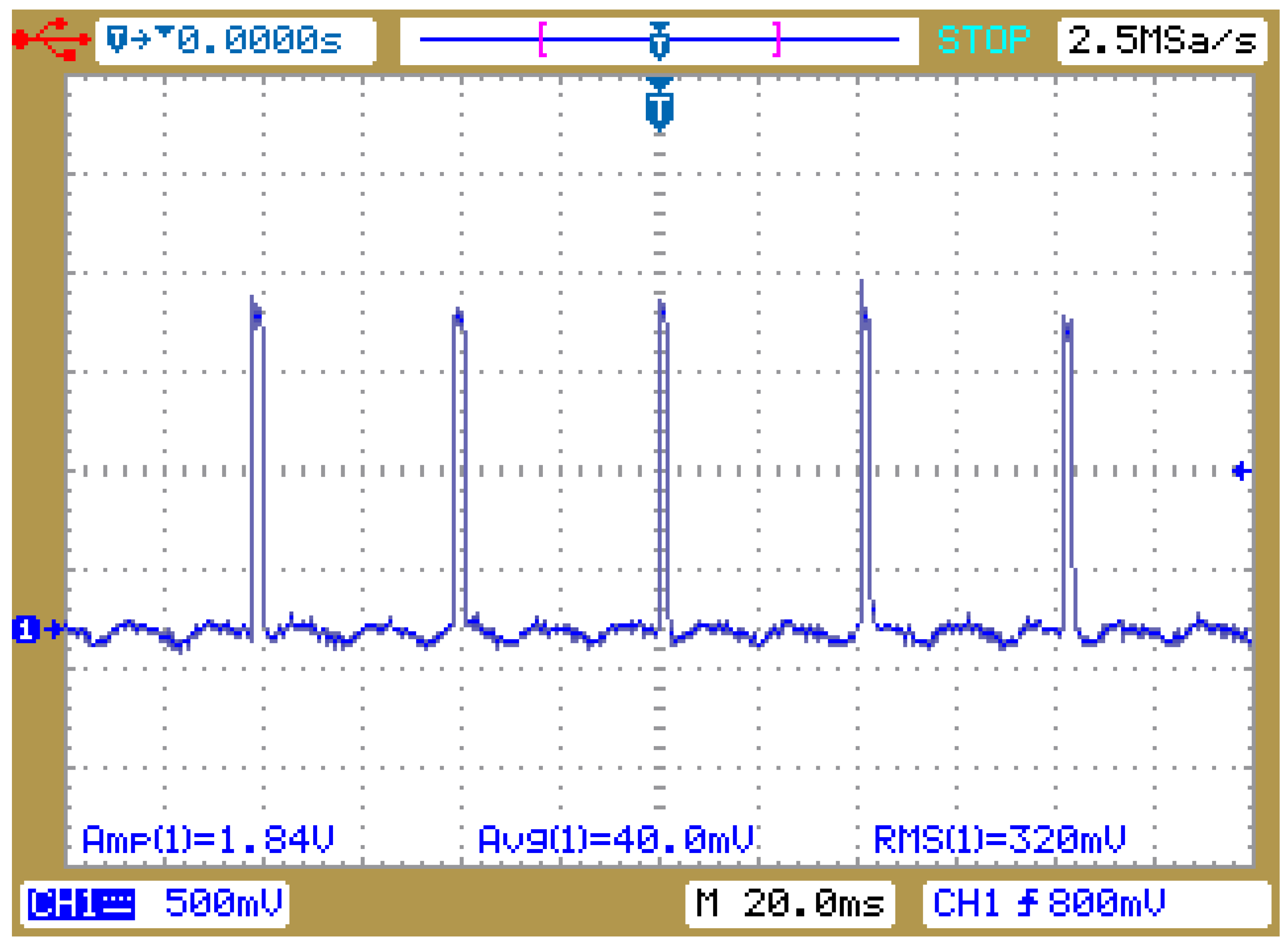
Figure 1 shows a WiFi signal in the time domain where the only observed activity corresponds to the beacon signal since no users are connected to the router. As observed, the BI is set to 40 ms, and with no traffic, they are visible “periods of silence” in the signal. Hence, in terms of available energy to harvest, the amount of it recovered from the environment will be relatively low [
19].
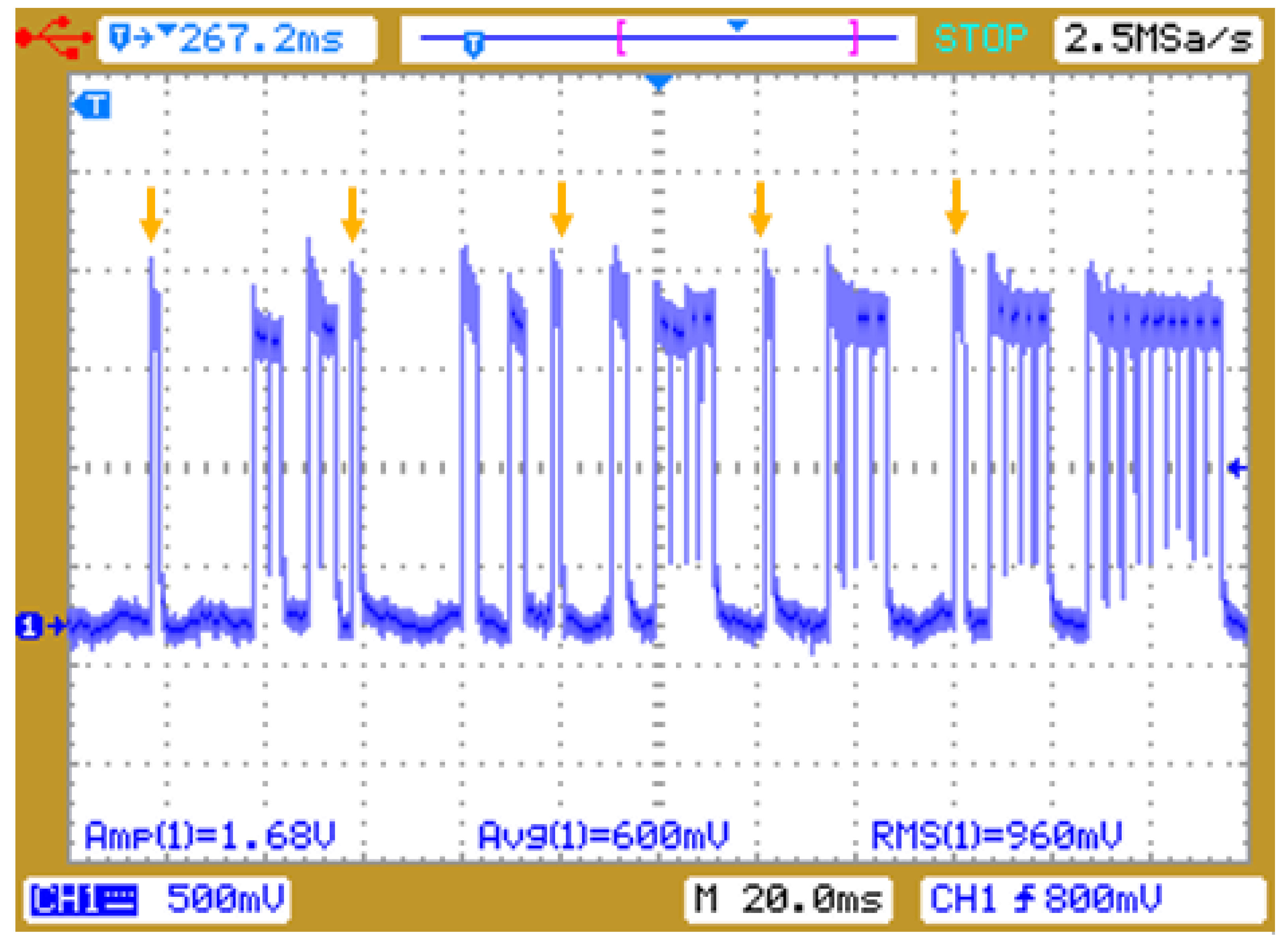
On the contrary,
Figure 2 shows the WiFi signal with the traffic demand by users connected. In this case, the beacon signal is identified by the arrows, where the BI is kept equal to 40 ms. If the BI is taken as the operation window for harvesting, it is clear that the WiFi signal can be viewed as a PWM-like signal; therefore, it can be concluded that more energy can be harvested with a significant amount of network traffic.
Another important parameter in the operation of WiFi technology is that it works by channels. There are 14 channels for the 2.4 GHz band, spaced 5 MHz apart, which distribute them from 2.04 GHz to 2.72 GHz. According to the geographical area, 11 or 14 channels are used. Thus, the configuration of 11 channels is used in America, from which Channels 1, 6, and 11 are primarily used. Usually, working with adjacent channels is not preferred because each channel occupies a BW of 22 MHz; therefore, overlap generates between them.
There is a metric known as RSSI (received signal strength indicator) in terms of received power. An RSSI is defined as excellent to good for data connectivity if its value is between −30 to −60 dBm; medium, between −60 to −75 dBm; low or very low, between −75 to −85 dBm; and no connection if the RSSI is below −85 dBm. However, even excellent and good RSSIs may not be sufficient from an energy-harvesting perspective since a signal of −40 dBm is equivalent to only 100 nW, which cannot be efficiently harvested. The latter is significantly more critical for WiFi technology, where the radiated power is variable according to the transmitted packets and not a constant or stable radiation source (See
Figure 1 and
Figure 2).
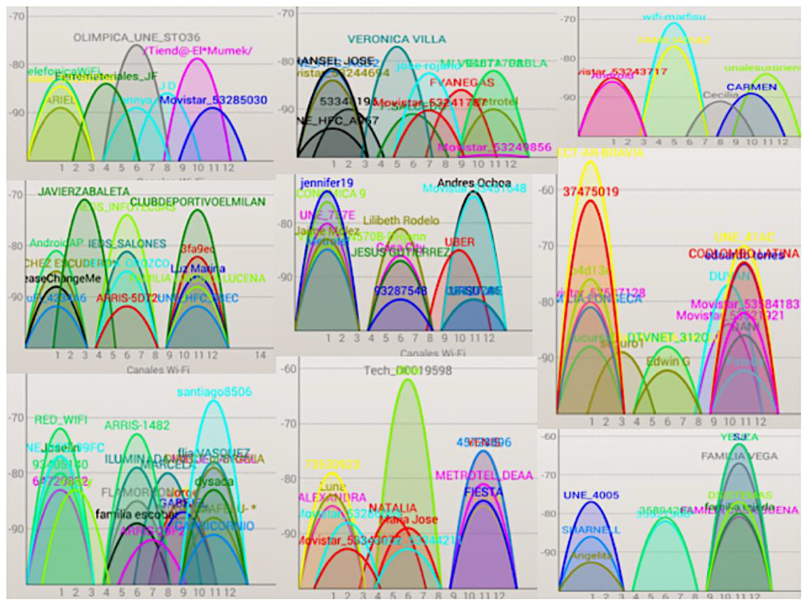
As shown in
Figure 3, the WiFi spectrum is packed for urban environments, and it can be thought that the several WiFi signals would add, allowing harvesting more energy. However, this would be only possible if such signals had considerable power levels and have the same frequency (i.e., constructive interference). It is important to note that levels below −40 dBm or −60 dBm only represent 100 nW to 1 nW. Thus, even if the signals add to each other, it would still be very little energy, a scenario that is illustrated in
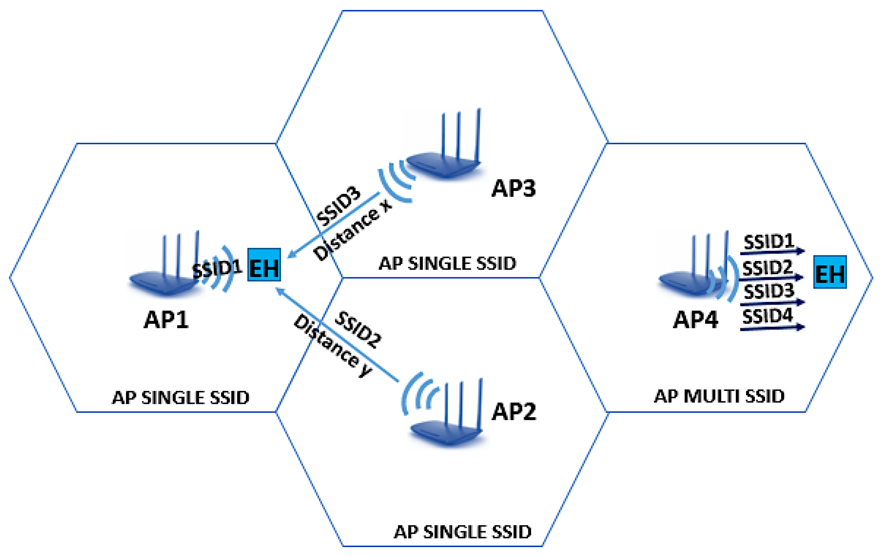
Figure 4 with APs 1, 2, and 3. This is the typical scenario in WiFi energy harvesting since it is unlikely to find APs installed at a single point or very close, making it difficult to take advantage of energy from all the equipment. Likewise, it must be considered that the antennas with higher gain (suitable for energy harvesting) are directive; therefore, not all the signals will fall within their aperture unless there is an arrangement or configuration of several antennas for this purpose.
The above provides a significant opportunity to target routers with multiple SSID characteristics that can simultaneously broadcast several wireless networks, perceiving themselves as 2, 3, or 4 carriers or different RF signals, as shown in
Figure 4 for the AP4. Thus, multiple SSID routers can be used to achieve more energy because signals effectively add up, and it is possible to maintain a level of energy harvesting even when there is no traffic on the network. Thus, if the operation window for harvesting is kept as the BI for a single SSID router (i.e., the operation window is kept the same for comparison); then, the BI for the other SSIDs becomes energy available for harvesting.
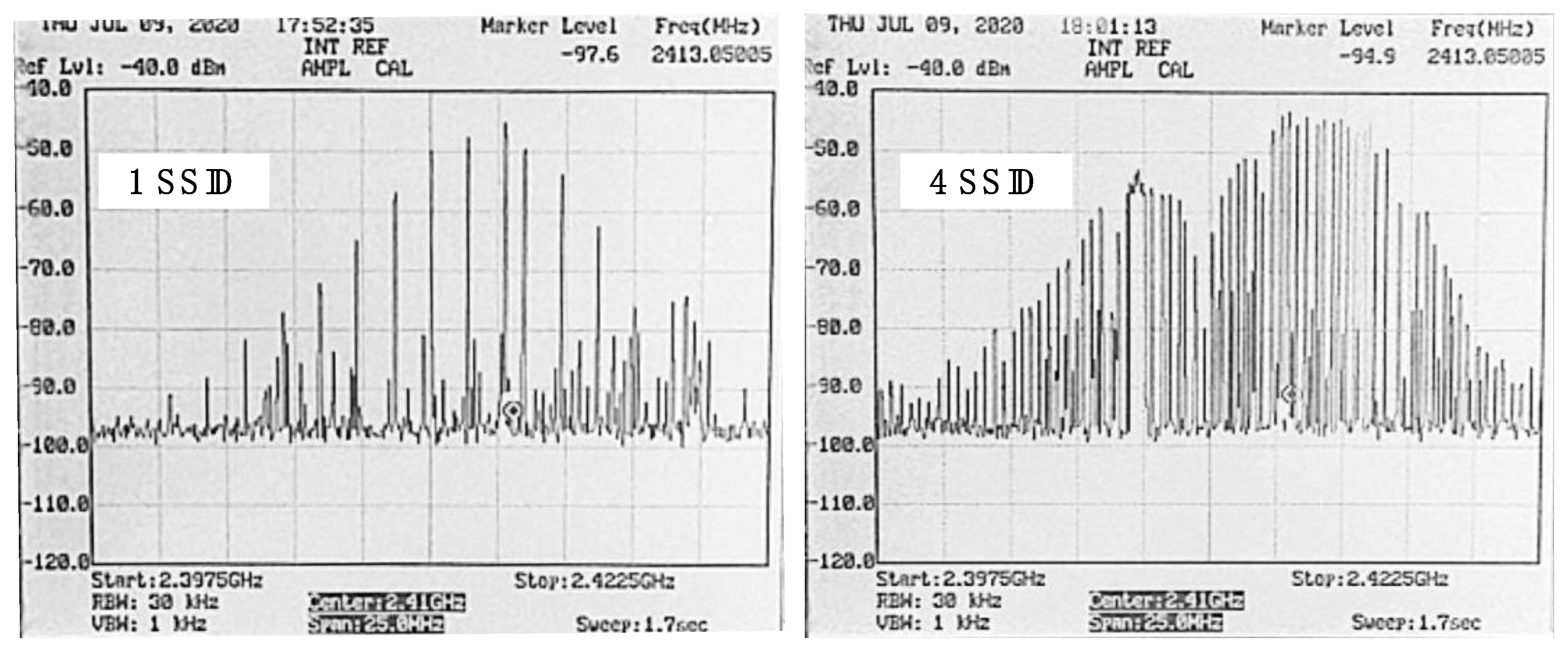
Figure 5 shows the harvester output signal exposed to WiFi signals with 1 and 2, 3, and 4 SSIDs, highlighting that the beacon signal for 4 SSIDs is equivalent to having a constant traffic rate a single SSID AP. This fact can be evidenced in measurements using a spectrum analyzer, as observed in
Figure 6, where a denser frequency spectrum can be observed at the 2.4 GHz band for multi SSIDs routers. The signal originating from a router with multiple SSIDs indicates that more power can be obtained for the same bandwidth.
3. Typical RF-EH Harvester System
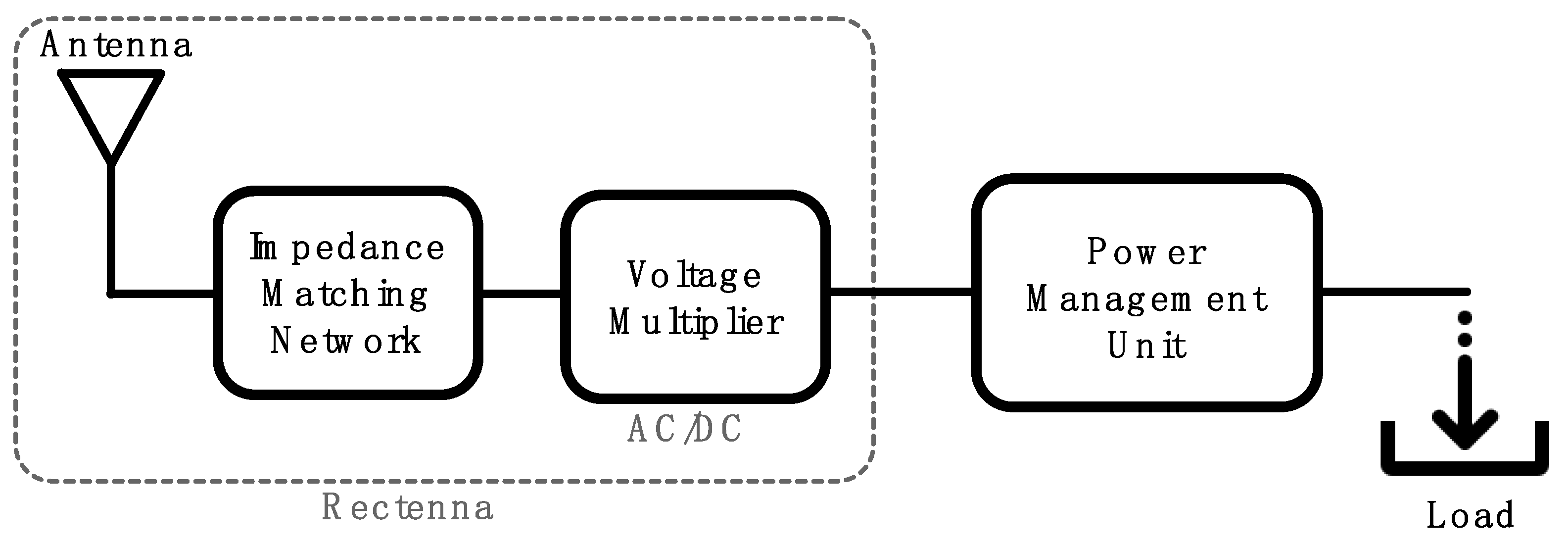
Figure 7 shows the essential components that comprise an RF energy harvesting system: antenna, rectifier, and power management circuit.
The antenna is the component that allows the capture of RF energy from the environment, which makes it the interface element between the harvester and the environment on which the RF energy is captured. For RF-EH systems, the predominant type of antenna is sector type. The most extensive use of these antennas is for mobile communications, such as WiFi, and they are used for limited-range distances. The antenna is designed taking as reference parameters such as gain, frequency, and bandwidth that define the amount of potential energy that could be harvested.
A block called impedance matching network follows, whose function is matching the antenna and rectifier/multiplier impedances looking for reducing the losses due to reflection (i.e., satisfy the maximum transfer power theorem).
Next, a rectifier is employed to single-polarize the perceived signal for DC conversion. Since the obtained DC component is low, the rectifier is complemented with a voltage multiplier (charge pump). The multiplier is described based on sensitivity, number of stages, output voltage, and conversion efficiency. There are several configurations of rectifier-multipliers. Among the most widely used are the Villard, Greinacher, Dickson, and Cockroft-Walton configurations [
21,
22,
23].
The antenna and rectifier/multiplier set are usually referred to as rectenna within the RF-EH literature. Proper design and interoperation of the rectenna blocks are essential to ensure high energy conversion efficiency (i.e., input and output powers as close as possible).
Finally, a power management circuit (PMU) guarantees suitable power conditions for the load given the energy harvested. For example, if the load requires a regulated or specific voltage or the load requires specific running times. According to the design constraints, a commercial or a tailored power management system can be employed. Finally, in terms of the energy storage units, supercapacitors are preferred in EH WiFi systems due to their power density characteristics associated with high loading and unloading speed, long-life cycle, size, and low cost compared to batteries [
24,
25].
3.1. Antenna Design Considerations
A basic antenna used in RF-EH systems based on WiFi is the patch type mainly because of its ease of PCB construction and its adaptability to different applications [
26,
27]. Other types of usable antennas are dipole, periodic log, and strip-loop [
26,
27]. An array of patch antennas can be used to improve the harvester antenna performance. The patch antenna is considered for the present work due to its simplicity of design and manufacture.
For the construction of patch antennas, Equations (1)–(4) are used to determine their dimensions according to the required parameters [
28].
Equally important are the return loss parameters (from the S-parameters), VSWR, and impedance adaptation. On the other hand, it is worth highlighting the effect of the incident power value within the performance of the system, which is defined for a transmission system according to Equation (5):
where
Pr is the power that reaches the receiver,
Pt is the power of the transmission system,
L is the losses associated with propagation in free space,
Gt is the gain of the transmitting antenna,
Gr is the gain of the receiving antenna (in this case the rectenna), λ is the wavelength at the operating frequency, and
d is the distance between the transmitter and the harvester.
Materials such as Rogers RO4350, RO3206, RO6010, and FR-4 [
29] are typically used to manufacture the antenna, the latter preferred due to its low cost and acceptable performance in the 2.4 GHz band [
28].
3.2. Voltage Multiplier Approach
Voltage multipliers are electronic circuits that allow to rectify an AC signal and convert it into a DC signal while increasing its voltage by a factor related to the number of stages of its construction, based on the combination of rectifier diodes and capacitors. The multiplier voltage output is given by Equation (6), where
Vi corresponds to the input voltage to the multiplier and
n to the number of stages that comprises it,
In RF-EH WiFi, the diodes must generate the lowest possible voltage drop to reduce losses. Thus, metal-semiconductor type (i.e., Schottky) diodes are preferred. This diode type is also widely used in RF-EH systems due to its working frequency of up to 24 GHz.
Equation (7) is used to evaluate the antenna and voltage multiplier performance, which corresponds to the power conversion efficiency and is given by the relationship between the incident power on the antenna and the power that can deliver at its output,
Along with the efficiency, the sensitivity is defined as the minimum incident power required for system operation, which is also adjusted to the load requirements [
30].
3.3. Power Management Circuit
An adequate PMU becomes crucial for proper sensor operation. As the total equivalent load changes, the supply system must provide a sufficient amount of power. DC-DC converters are circuits that convert a DC voltage to a different DC regulated level with high efficiency (>80%). According to the application, the DC-DC converters can increase or reduce the output voltage compared to the input voltage. Some are also designed to find the maximum power point (MPP) [
31].
Given the WiFi signal nature, it is expected to require high charging/discharging rates, which imposes speed requirements for a storage unit. Batteries can be an option; however, the load probably could be inoperative for an extended period before use it. In this case, the speed requirement for the storage unit can be satisfied with supercapacitors (SCs), if the loads to be fed with the harvested energy are selected to be ultra-low power. Thus, defining the energy stored by a supercapacitor as
and considering a load working a 3.3 V and a SC equal to 220 mF, it is possible to feed a load requiring 300 μW constantly for an hour. Thus, it is perfectly feasible to feed an IoT temperature sensor with the SC stored energy. It is important to determine if that amount of energy can be obtained from a WiFi signal radiated from an ordinary router (multi SSID, as commented).
4. System Description
4.1. Antenna Design Concept
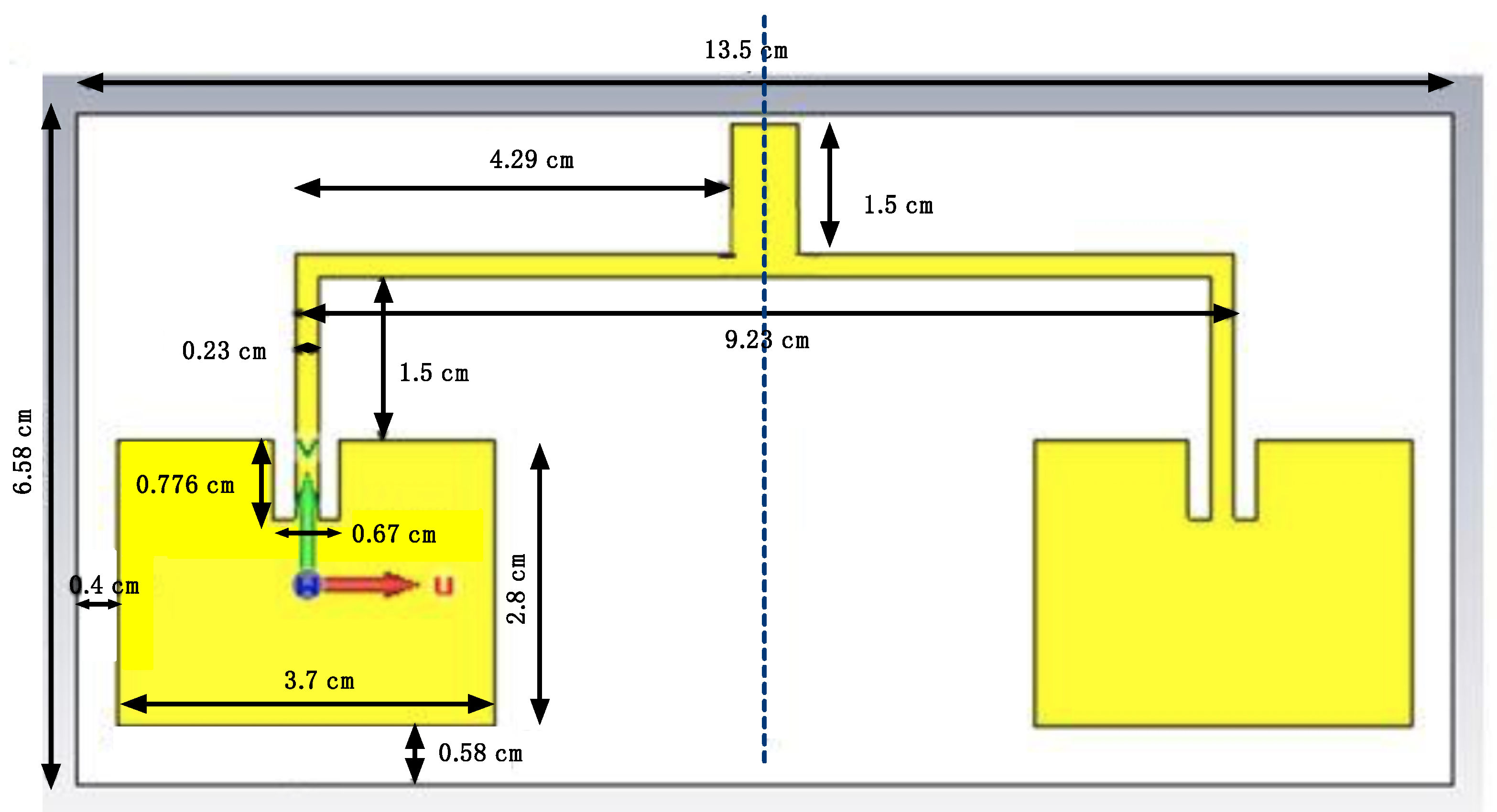
Given the low power received from an ordinary router and the ease of building patch antennas, it is decided to work with a 2 × 1 array to keep the footprint as small as possible. The dimensions and geometry of the array are shown in
Figure 8. The total area for the 2 × 1 array equals 88.8 cm
2.
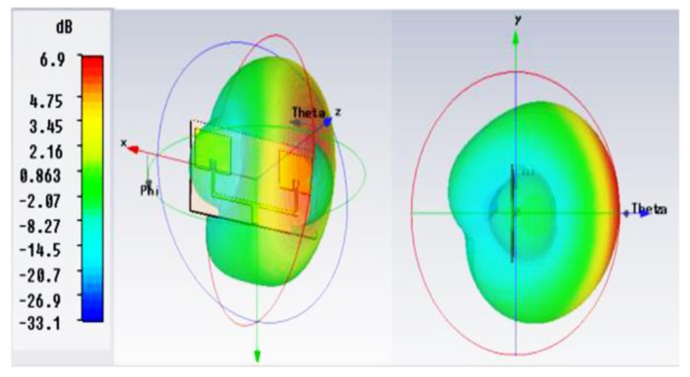
The design of the antenna array is carried out using the CST software. This tool contains a module that allows adjusting antenna dimensions until it centers the desired frequency of operation. The design process started from a rectangular patch obtaining a gain of 3.7 dB; then, configuring an array, a total of 6.9 dB is reached, allowing higher energy harvesting than the single patch (see
Figure 9). Even though more patch antennas can be added to configure a bigger array, extra patches increase the antenna footprint, which cannot be attractive for IoT modules. As observed, the patches are lined up vertically so that it agrees with signal transmission polarization.
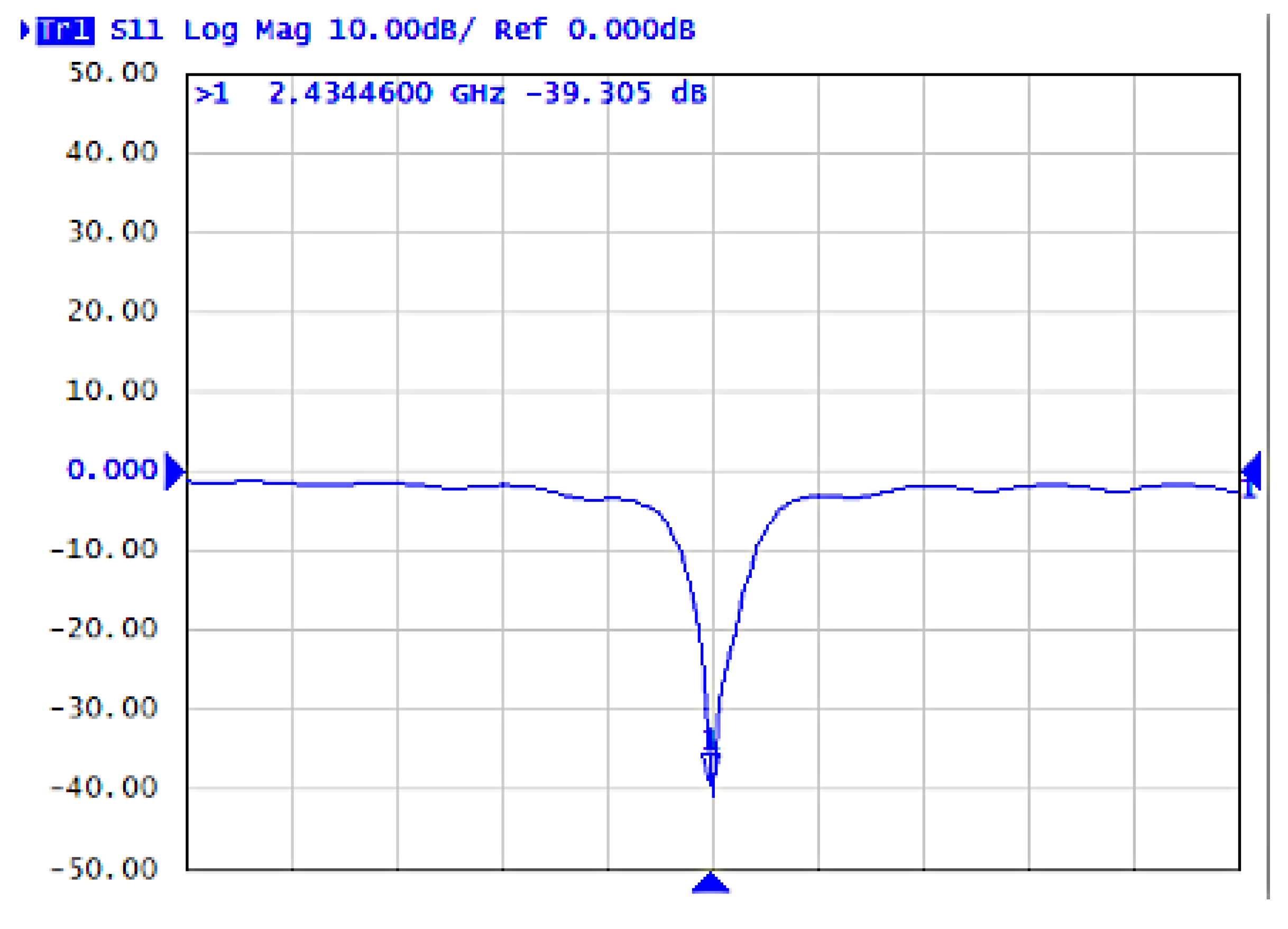
The simulated S
11 parameter shows −43.19 dB, which guarantees the highest incident RF signal capture. It can be observed a 78% coverage of the 2.4 GHz WiFi band defining a −10 dB bandwidth, which allows having optimal behavior in 2.437 MHz equivalent to Channel 6.
Figure 10 summarizes the simulated performance of the 2 × 1 array.
4.2. Multiplier Design Concept
From the literature, it is possible to design the rectenna without an impedance coupling network between antenna and multiplier.
When there are non-linear circuits like the rectifier, the impedance matching becomes dynamic since the impedance of these circuit changes with the input power and frequency. Therefore, the case can be further complicated if the load circuit is also non-linear since its impedance would change with the same parameters. In general terms, the load coupling process is influenced by component-value tolerances, errors associated with manufacturing processes, among others [
32].
A determining factor in the voltage multiplier corresponds to the number of stages that make it up. The output voltage and input sensitivity are defined as the device can harvest energy from the WiFi signal. Therefore, performance evaluation is required according to the frequency of use, incident power, and load. Based on the analysis developed in [
23], from three multiplier topologies (Dickson, Cockroft-Walton, and Greinachert), the Cockroft-Walton type multiplier is chosen.
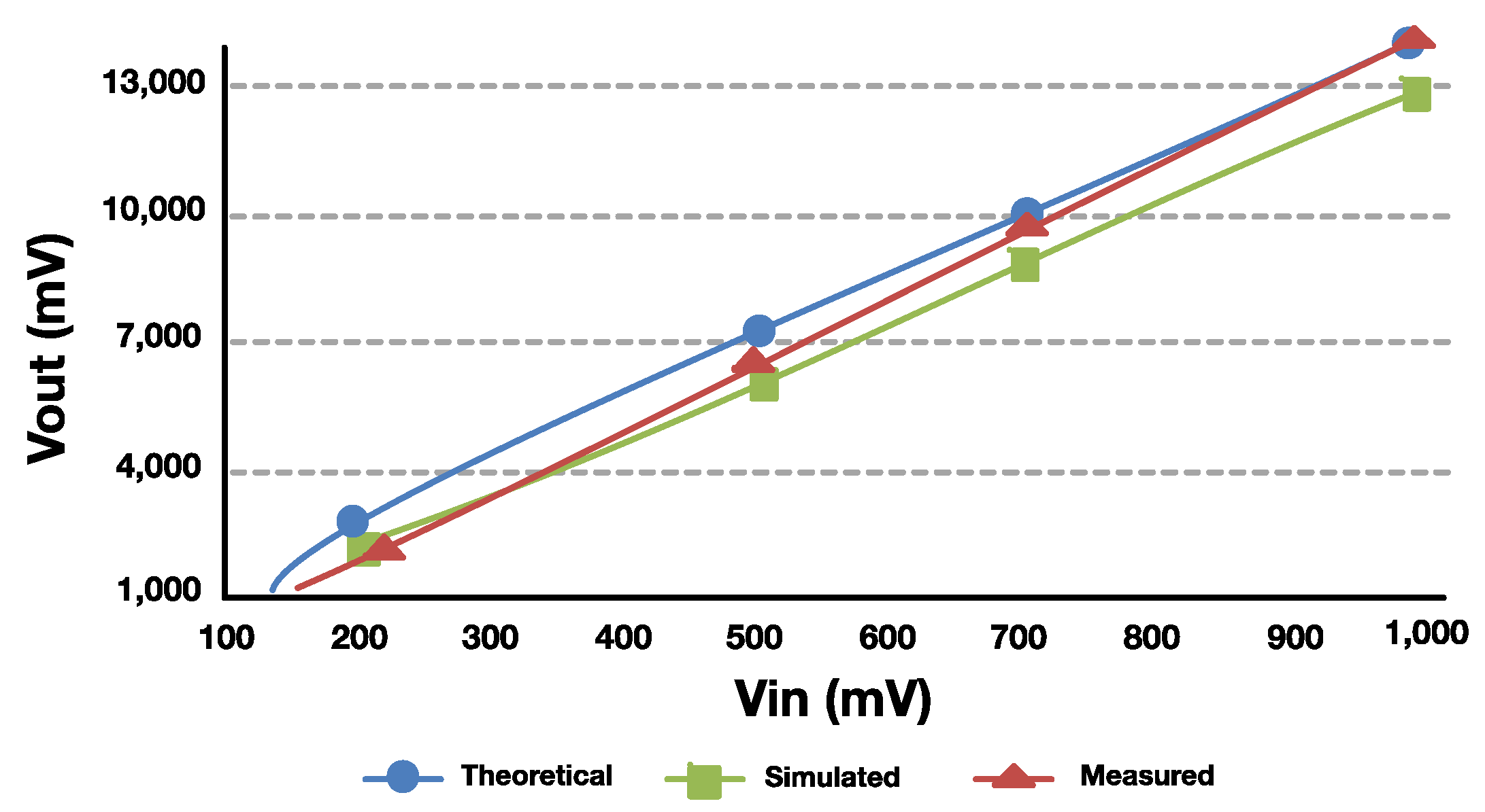
Experimental tests are carried out with voltage multipliers of 4, 5, 6, 7, and 8 stages, and the performance of each one is evaluated to define the number of stages. As commented, Schottky diodes are selected to reduce voltage losses.
According to the simulations, the higher the number of stages, the higher the voltage output; however, in practice, from a determined number of stages, no improvement in the output will be obtained due to the little amount of available energy at the input affecting the conversion efficiency. Therefore, the number of stages with the best possible performance must be determined via testing.
4.3. PMU Proposed Architecture
For the present application, a commercial device could be used as a PMU. These available units have functions such as managing the charging and discharging of storage devices, providing a regulated supply voltage to the components, and even generating an alarm when the energy storage element approaches the end of its useful life [
31]. However, given the WiFi signal behavior, the present work proposes a switching unit using SCs that can maximize the energy from the PWM-like waveform of WiFi and is sensitive enough to respond to reduced time intervals such as the BI. Thus, the energy available for the load or a following PMU, if required, is improved.
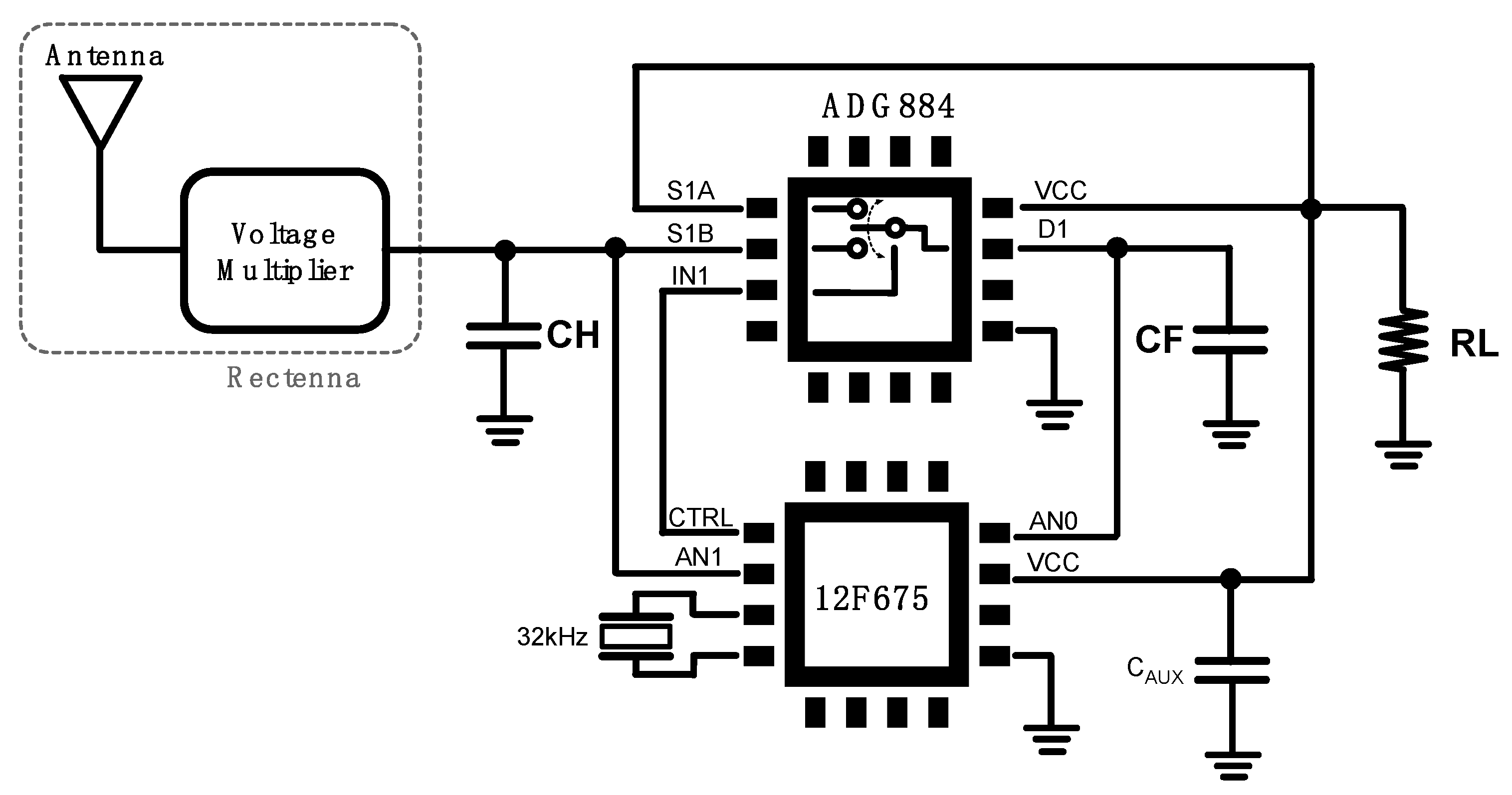
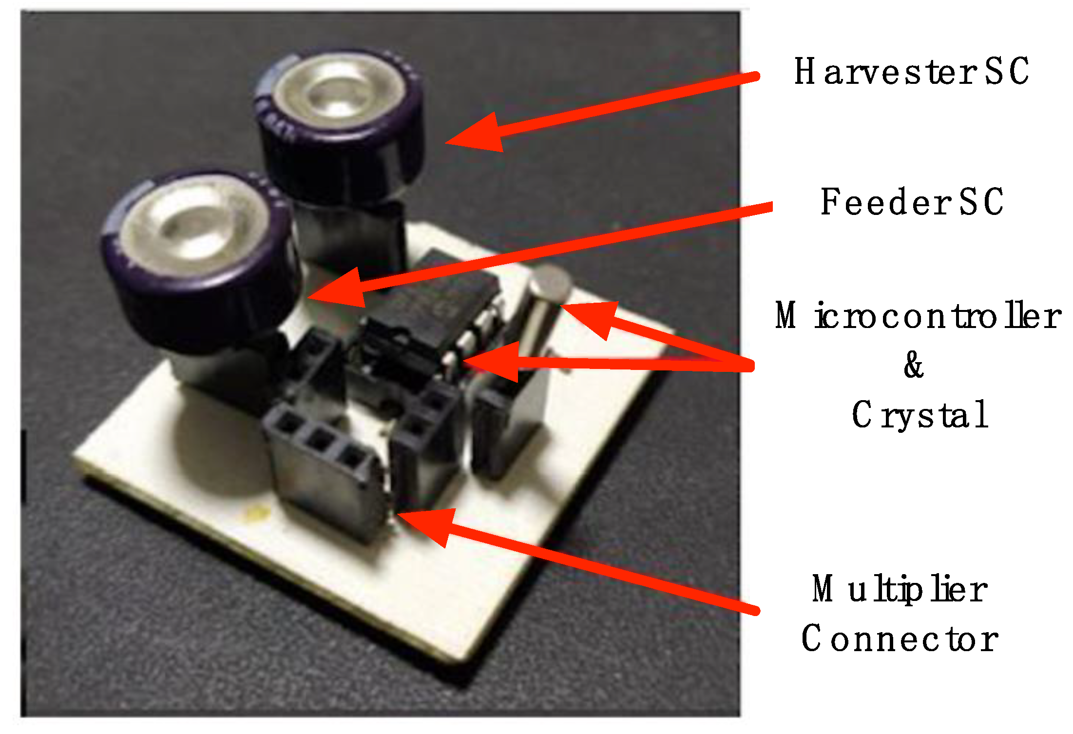
The switching scheme proposed is shown in
Figure 11. The operation of the system is based on the charge-discharge cycle of the two SCs. An SC, identified as
CH or harvester capacitor, remains connected to the rectenna charging with the harvested energy. A second SC, labeled as
CF or feeder capacitor, supplies power to the load (connected at S1A). The two SCs are controlled by an SPDT-type electronic switch (ADG884) governed by a microcontroller (12F675). The microcontroller compares the two capacitors voltage values to generate a switching command to the SPDT to allow the transfer of energy from
CH to
CF when a sufficient amount of energy Δe is available at
CH. For recharging,
CF is disconnected from the load during a time
t (time necessary to guarantee the passage of energy) and connected to
CH. After the time
t has expired, the elements return to their previous connections. Thus,
CH receives power from the rectenna again; however, the charging will not start from zero but the prior-step residual charge.
CF returns to supply energy to the load but with a higher Δe value than the beginning of the commutation.
A microcontroller is chosen to govern the switching process of the two SCs to ease the switching instant selection, allowing greater versatility and future improvements in the load exchange scheme programming. According to requirements, the 12F675 microcontroller is selected due to its low power consumption, availability of a standby mode, voltage comparators, reduced footprint, and pin configuration. The idea is that the use of harvested energy is minimally spent on the operation of the microcontroller. In low power mode (LP), the 12F675 draws a current of about 8.5 μA at 2 V voltage when set to LP mode. Therefore, since the ADG819 switch has a consumption of 500 nA, the consumption estimate for the proposed power management circuit is approximately 18μW.
Thus, according to the typical charging/discharging process,
Figure 12 describes the time-domain behavior of the two SCs (
CH and
CF). As observed, there are two previous processes before the proposed scheme can start normal operation, Charging
CH and Building up in
CF.
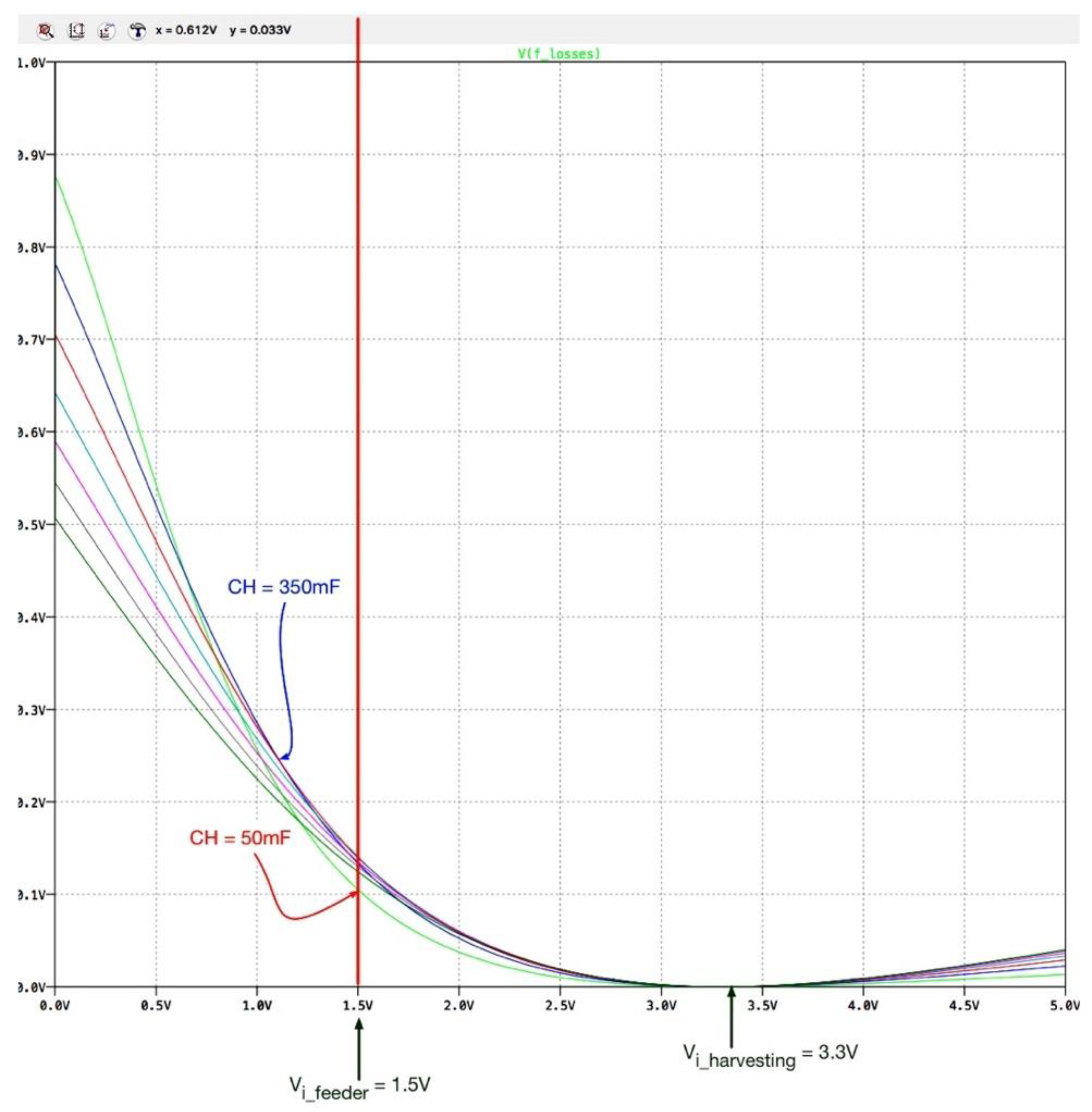
Once the Normal Switching Operation is reached, it can be observed that four parameters need to be defined. Vi_harvesting corresponds to the maximum voltage that it is expected to have during charge in CH; Vf_harvesting is the final voltage observed in the CH after transferring energy. Similarly, Vi_feeder identifies the minimum voltage that can appear in CF after a load supplying cycle is carried out, and Vf_harvesting is the voltage reached after charging from CH. The selection of those parameters is important so that losses in the energy transfer process are minimized.
According to [
33], the fractional losses in the process of energy transfer between capacitors can be expressed as
and Equation (9) applies when the voltage across both capacitors finally is the same. Although the proposed scheme is not expected to reach the same voltage in both capacitors, Equation (9) still provides a design criterium for minimizing losses in the process even if the energy transfer is partial. Reference [
33] shows the generic plot of Equation (9) and states that fractional losses are minimized when both capacitors are the same. However, since the same voltage is not reached in this proposed case, this statement does not apply the same; therefore, it would be shown that different values of capacitors actually produced better results.
Testing will be carried out to evaluate the operation of the scheme, and circuits including LC-like circuits could be employed for improved efficiency. For now, the circuit is kept as simple as possible for demonstration purposes.
6. Conclusions
This work presents an energy harvester for a 2.4 GHz WiFi MultiSSID router, which exhibits an estimated efficiency of 50.18% over an incident power of 0 dBm. The harvester has been designed based on the analysis of WiFi signals, and, through empirical testing, it has been possible to remove an impedance matching network due to the measured impedances for the proposed versions of the antenna and the voltage multiplier. Thus, the system complexity has been reduced without sacrificing performance. The harvester has been completed with a PMU module that simultaneously provides charge to the load and harvests energy from WiFi via a switching scheme. Such scheme is controlled by a low-power microcontroller that can work with supply values as low as 1.5 V and current drawing of about 18 μA. The switching scheme adjusts to the PWM-like nature of the WiFi signal and provides rapid power availability for load operation. The advantage of using a microcontroller-based switching scheme lies in the possibility of adjusting through programming the switching threshold to minimize losses in the charging losses between two SCs that serve as storage units.
The built prototype shows that thanks to a basic analysis of the WiFi signals, it is possible to have the required amount of energy for a sensor operation from a multiple SSID router. It is important to note that the router employed does not require additional modification but the BI to be used as a source generator.
As future work, it is possible to optimize the antenna to reduce its dimensions, increase its gain, and improve the conversion efficiency on power less than −5 dBm. Regarding the PMU, the objective is to continue improving its performance in terms of minimizing losses. This work can be done on three fronts; one, to optimize the selection of capacitors CH and CF; second, to work with adjustable and adaptive switching thresholds; and finally, to explore LC circuits to increase energy transfer efficiency.
Besides, it is also possible the implementation of D2D encryption mechanisms such as the one proposed in [
6] thanks to the availability of an on-board microcontroller.


