Article

Enabling Energy-Efficient Physical Computing through Analog Abstraction and IP Reuse

Electrical and Computer Engineering (ECE), Georgia Institute of Technology, Atlanta, GA 30332-250, USA
*
Author to whom correspondence should be addressed.
J. Low Power Electron. Appl. 2018, 8(4), 47; https://doi.org/10.3390/jlpea8040047
Submission received: 1 October 2018 / Revised: 12 November 2018 / Accepted: 16 November 2018 / Published: 24 November 2018

Abstract

:
This paper shows the first step in analog (and mixed signal) abstraction utilized in large-scale Field Programmable Analog Arrays (FPAA), encoded in the open-source SciLab/Xcos based toolset. Having any opportunity of a wide-scale utilization of ultra-low power technology both requires programmability/reconfigurability as well as abstractable tools. Abstraction is essential both make systems rapidly, as well as reduce the barrier for a number of users to use ultra-low power physical computing techniques. Analog devices, circuits, and systems are abstractable and retain their energy efficient opportunities compared with custom digital hardware. We will present the analog (and mixed signal) abstraction developed for the open-source toolkit used for the SoC FPAAs. Abstraction of Blocks in the FPAA block library makes the SoC FPAA ecosystem accessible to system-level designers while still enabling circuit designers the freedom to build at a low level. Multiple working test cases of various levels of complexity illustrate the analog abstraction capability. The FPAA block library provides a starting point for discussing the fundamental block concepts of analog computational approaches.

1. Motivation and Need for Analog Abstraction

Although developing abstraction of analog is considered an unlikely dream, this paper shows the first step in analog (and mixed signal) abstraction utilized in large-scale Field Programmable Analog Arrays (FPAA), encoded in the open-source SciLab/Xcos based toolset (
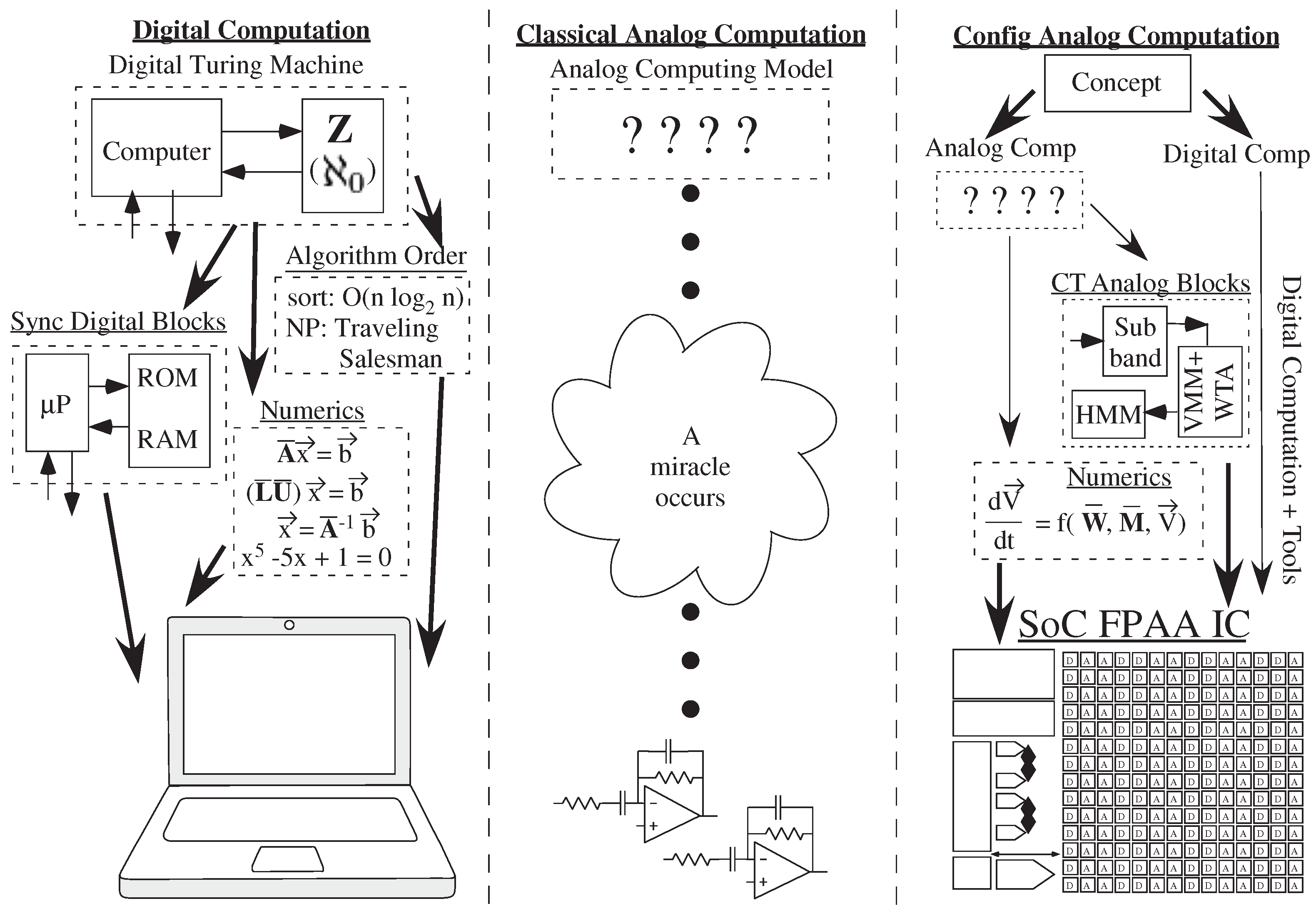
Figure 1). Often, individuals often state confidently that developing a hierarchical representation for analog circuits and systems is incredibly difficult, unlike the simple digital circuit and system representation, even those trained in analog design. Analog systems require so many different circuit combinations, with many detailed and complicated decisions. Digital systems are naturally hierarchical, composed from NAND or NOR logic gates, multiplies and addition units, and a range of processors with associated memories. Digital, as currently taught, naturally moves from device to circuit to Gate to Module to System., and analog just seems nearly impossible to make a similar story.
Are digital systems naturally hierarchical, and is analog processing nearly impossible, or are the perceptions a product of historical development? Digital required hierarchy and a computational framework (e.g., [1]) in its early development (1940s and 1950s) to compete with existing physical (e.g., analog) computing devices, a framework that allowed it to accelerate through the Moore’s law [2,3] and VLSI design [4] eras, in order to become the usual computational choice today (Figure 2). Analog computation was less and less used or taught in education. Without significant analog implementations available, particularly those accessible to some non-analog Integrated Circuit (IC) designers, any discussion of analog computation is effectively theoretical.
Traditional analog system design and computing still resembles its roots in the 1950s and 1960s, where every problem is hand crafted by a circuit expert to create a miraculous solution (Figure 2). The design often tends to be bottom-up, and reuse of previous solutions and approaches is not common. Such approaches don’t enable wide-spread development using these techniques, unlike the wide use of digital design techniques.
Analog computation [5] becomes relevant with the advent of FPAA devices (Figure 2), particularly the SoC (System on Chip) FPAA devices [6] and resulting design tools [7] (Figure 4). FPAA requires an analog computation framework (Figure 2) to reach its large potential. The discussion of resolution and computational noise and computation energy has recently been addressed [8], showing a balance between analog and digital computation, each with their own optimal regions. Analog abstraction and hierarchy, including the capability of top-down analog computing, is fundamental for practical analog computation.
The abstraction and tool framework will focus on the SoC FPAA family of devices, although the techniques would be applicable to other FPAA devices, as well as applicable to general analog implementations and other real-valued (physical) computing systems. Analog abstraction will focus on algorithmic abstraction, such as filtering, subband processing, and classification, as the analog equivalent of multiply and addition tend to be circuits requiring simply one (or a few) transistors per input vector component [9]. These presented techniques are only the beginning of these directions.
This discussion presents the first step in analog (and mixed signal) abstraction utilized in an FPAA encoded in the open-source SciLab/Xcos based toolset. Reviewing the SoC FPAA ecosystem and energy efficiency discussions (Section 2) provides the background for developing abstraction. This background enables developing design approaches for abstraction and resulting library blocks (Section 3). We instantiated abstraction in tools (Section 4) is split into system design (Section 4.1) and circuit level design (Section 4.2) with a transition between levels. The SoC FPAA approach is aimed primarily for system design while still enabling circuit level design. The discussion then proceeds to show the abstraction and complexity of multiple working test cases, illustrating analog abstraction capability (Section 5). We conclude by discussing the FPAA block library (Section 6), discussing the implications for the existing library as well as speculation on fundamental block concepts of analog computational approaches.

2. Energy Efficiency and SoC FPAA Ecosystem

This discussion will develop the start of an analog and mixed signal abstraction resulting from a number tool efforts required for system-level FPAA design. Design tools are a practical instantiation of abstraction (Figure 1). Analog computing enables both improved computational efficiency (speed and/or larger complexity) of ×1000 or more compared to digital solutions (as predicted by [9]), as well as potential improvements in area efficiency of ×100. Multiple analog signal processing functions are a 1000× factor more energy efficient than digital processing, such as Vector-Matrix Multiplication (VMM), frequency decomposition, adaptive filtering and classification (e.g., [6] and references within). Biologically-inspired classifier techniques open the opportunity for configurable biologically-inspired, energy-efficient classifier approaches (1,000,000× over custom digital solutions) [10] for context-aware applications.
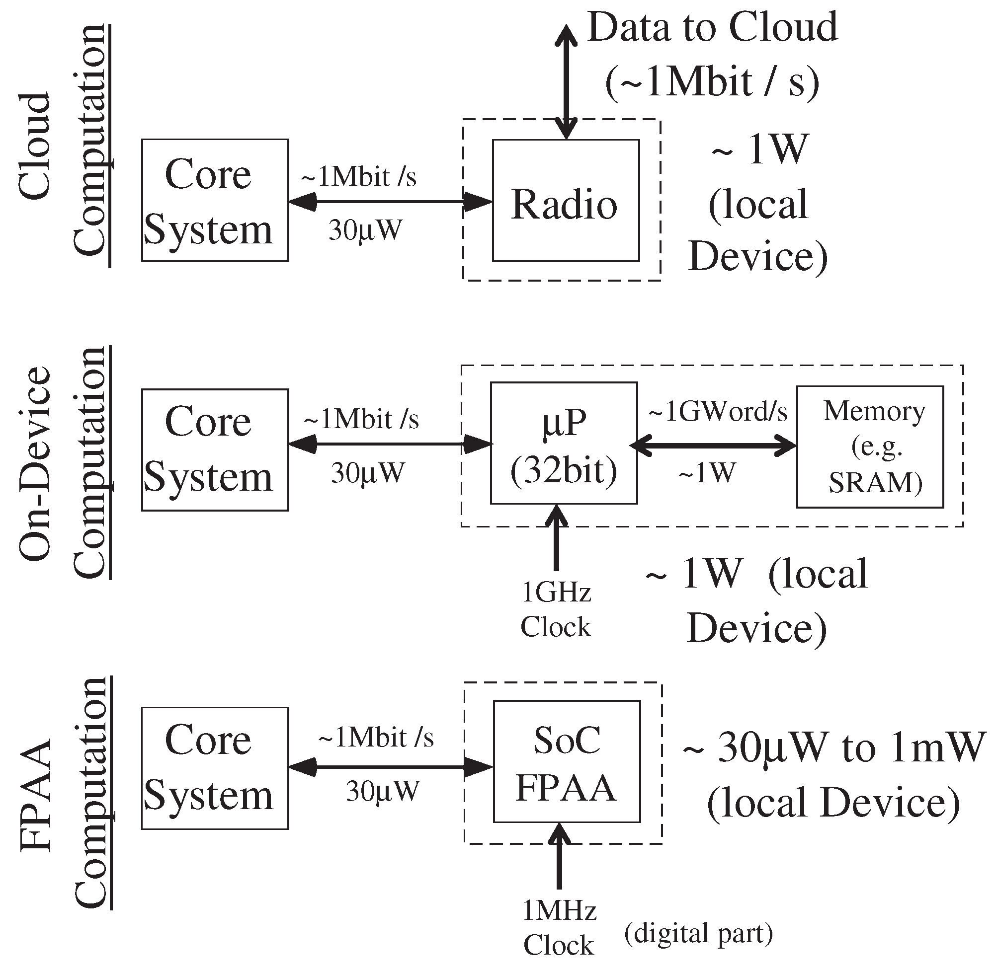
Figure 3 illustrates the energy impact for cloud computation, on-device digital computation, and FPAA assisted computation. Many portable and wearable devices are constrained by their energy-efficiency. Digital communication typically dominates the overall energy consumption [10]. Cloud based computing removes issues of real-time embedded (e.g., fixed point arithmetic) to be done on some far away (and supposedly free) server using MATLAB-style coding, a high-level language utilizing double-precision numerics where the numerical algorithms are already developed. Computation done off of the device is not seen, and considered effectively endless, eventually resulting in energy and resulting infrastructure required still has significant impacts. The host system still must constantly transmit and receive data through its wireless communication system to perform these computations. The network connectivity must have a minimum quality at all times; otherwise, performance noticeably drops. One often assumes that the cloud is nearly free for a small number of users. As the product scales to the consumer market, these assumptions can break down. Although the local digital device computation (for a good wireless network) requires similar energy for cloud and on-device computation (at a 100MMAC(/s) level), physical computation, such as FPAA empowered devices, enables factors of 1000× improvement in the overall power requirements.
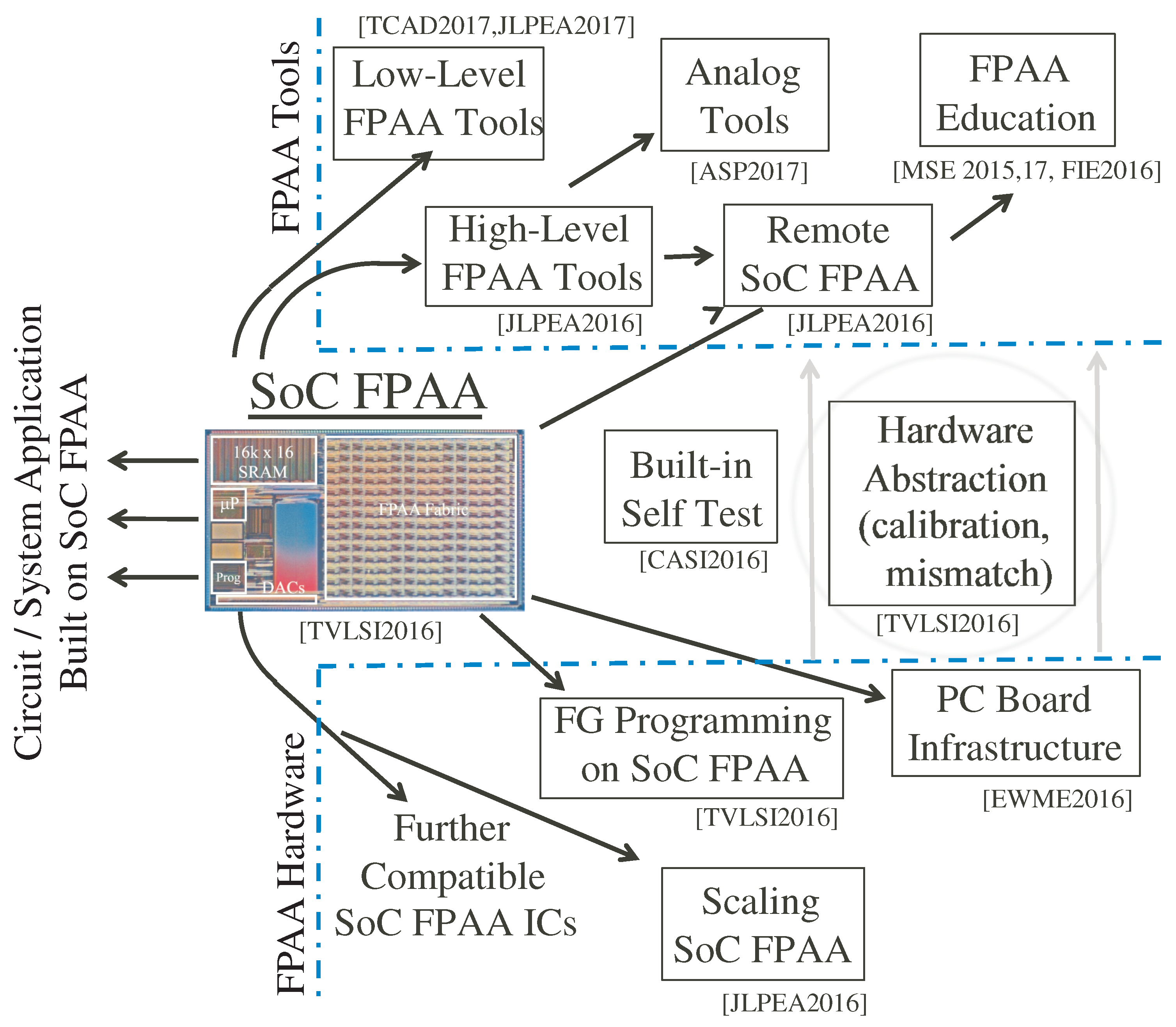
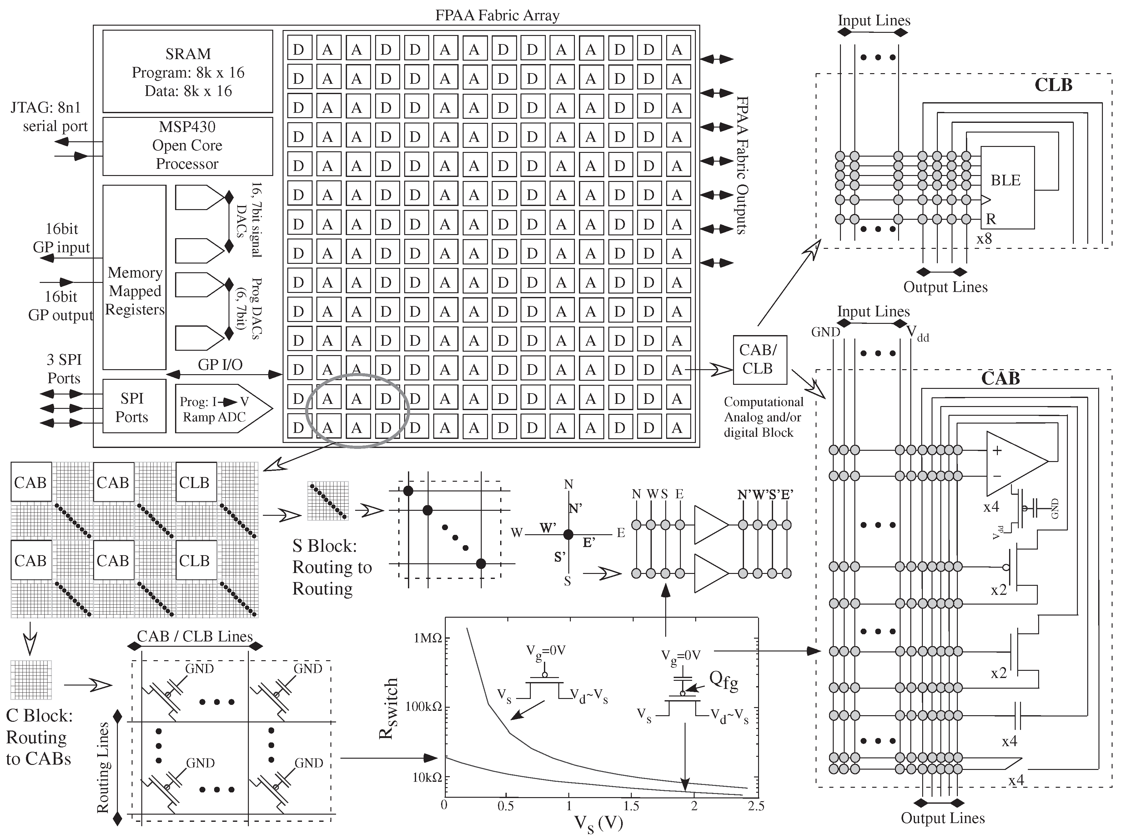
The SoC FPAA ecosystem (Figure 4) is built around the SoC FPAA family of devices, such as [6], providing user-friendly infrastructure for system design. The infrastructure could be utilized for the earliest of FPAA devices (e.g., [11]). These FPAA devices use Floating-Gate (FG) devices for ubiquitous small, dense, non-volatile memory throughout the 350 nm CMOS IC. SoC FPAA devices can scale to smaller IC process nodes with improved energy efficiency, increased bandwidth/clock rates, and reduced system area, all improving quadratically with decreasing linewidth [12] We expect future FPAA devices to be built to this standard. Early recognition of FG switches (e.g., Computational Analog Blocks (CAB) selection crossbars) as computational elements [13] both enabled a wide range of computations (e.g., VMM [14]), as well as brought creative energy to the routing infrastructure (history described in [6]) and resulting system capabilities. In such architectures, the CAB components are often the boundary conditions for the computation, not the core computation.
Over a decade of consistent FPAA development and application design has roughly converged on a typical mixture of several medium level components per CAB (OTAs, FG OTAs, T-gates), along with a few low level elements (transistors, FG transistors, capacitors). Comparing the CABs of early papers [11] to the CAB topology of recent FPAA designs (Figure 5, adapted from Figure 2 in [6]) shows some similar characteristics, validated by numerous circuits designed and measured in these architectures. A few CABs might be specialized for larger functions (e.g., signal-by-signal multipliers [6], sensor interfacing [15], neurons [16]), showing their relative importance in these discussions. Most of these elements have at least one FG parameter that is part of the particular device used. For small to moderate CAB components, the complexity of the resulting device is roughly proportional to the number of pins available for routing. Three terminals of an nFET transistor has similar system complexity to three terminals of an FG OTA. We expect some small shifts in these components in future FPAA devices, such as dedicated current-conveyer blocks, but generally, the CAB level components are stable. The number and size of FPGAs Look Up Tables (LUT) vary from architecture to architecture; FPAA CABs vary similarly.
FG circuits enable a large potential circuit design space that can be tuned around mismatches (e.g., [17]). All Transconductance Amplifiers (OTA) have an FG transistor to set its bias current; the bias current can be directly programmed between 50 pA and 10 μ A with better than 1% accuracy at all current levels [18]. FG OTAs are chosen for programming input offsets (FG charge) as well as programming the linearity (capacitor elements) and open-loop gain of the OTA. For many applications, one considers the OTA devices as a differential-input, voltage-output amplifier.
The SoC FPAA [6] ecosystem represents a device to system user configurable system. An SoC FPAA implemented a command-word acoustic classifier utilized hand-tuned weights demonstrating command-word recognition in less than 23 μ W power utilizing standard digital interfaces [6]. Multiple analog signal processing functions are a factor of 1000× more efficient than digital processing, such as Vector-Matrix Multiplication (VMM), frequency decomposition, adaptive filtering and classification (e.g., [6] and references within). Embedded classifiers have found initial success using this SoC FPAA device towards command-word recognition [6], and accoustic (and biomedical) sensor classification and learning (e.g., [19]) in 10–30 μ W average power consumption. Floating-Gate (FG) devices empower FPAA by providing a ubiquitous, small, dense, non-volatile memory element. The circuits compute from sensor to classified output in a single structure, handling all of the initial sensor processing and early stage signal processing. This ecosystem scales with newer ICs built to this standard, as expected by all future FPAA devices [12]. The μ P is clocked at 20 MHz, and can be clocked at least to 50 MHz, consistent with other digital computation in 350 nm CMOS; at smaller linewidth processes, the highest clock rate increases.
Figure 4 shows a high level view of the demonstrated infrastructure and tools for the SoC FPAA, from FG programming, device scaling, and PC board infrastructure, through system enabling technologies as calibration and built-in self test methodologies, and through high level tools for design as well as education. The current infrastructure enables a discussion of the analog block abstraction.
This ecosystem and abstraction allows us to talk about approaches for future FPAA devices in scaled down technologies (e.g., 130 nm and 40 nm) [12]. Development of FPAA devices in 350 nm CMOS has enabled a powerful platform to iterate on FPAA designs, while still having several engineering applications. One expects future FPAAs in a range of processes for a range of bandwidths and clock frequencies. The development of a 40 nm SoC FPAA device [20] showed that FG enabled analog and digital design is fairly similar to design at the 350 nm node. The FG devices eliminate most issues of threshold voltage mismatch, the primary issue in porting analog and digital designs to 40 nm and smaller device nodes. Avoiding threshold voltage mismatch by FG devices breaks the typical viewpoint that one wants large transistors for analog as opposed to using small transistors for digital operation. Smaller voltage headroom and lower transistor gain need to be considered for any design, where the drop from 2.5 V supply at 350 nm FPAA to a 1 V supply at 40 nm is a small effect, particularly for circuits operating with subthreshold bias currents. Transistors at 40 nm CMOS are mostly operating with subthreshold or near subthreshold bias currents. As a result, one expects little change in device modeling or in system abstraction scaling between 350 nm and 40 nm CMOS that likely continues when scaling to smaller process nodes. The device and circuit modeling would be similar, although the simulation parameters would likely change for a new IC process (350 nm → 40 nm). One can also utilize digital devices to assist with any analog functionality as a result of scaling, just as one can utilize more analog devices to assist with numerical computation.
The open-source toolkit is a developed Analog-Digital Hardware-Software CoDesign environment for simulating and programming reconfigurable systems [7]. The analog (and mixed signal) abstraction is developed in this open-source toolkit used for the SoC FPAAs. This tool simulates, designs, as well as enables experimental measurements after compiling to configurable systems in the same integrated design tool framework. The simulation tool enables current-voltage and individual transistor level simulation, as well as abstracted system-level simulation. High-level software, x2c, in Scilab/Xcos (open-source clone of MATLAB/Simulink) converts high-level block description by the user to a modified blif ( Berkeley Logic Interface Format) format, verilog and assembly language. This tool uses modified VPR [21] code for global place and route while utilizing its own code for local place and route functions. The resulting targetable switch list is targeted on the resulting configurable analog–digital system.

3. Tool, Abstraction, and Initial Block Library Design Approach

One might wonder if fundamental analog building blocks, both in hardware and in the software tools, can be reasonably determined in a similar way one uses look-up tables and flip-flops for FPGA designs. Digital FPGA components did not start off being obvious, starting with Programmable Array Logic (PAL) and Programmable Logic Array (PLA) approaches. The approaches used came from the same individuals who were working on look-up tables and and-or logic components. There was not a methodology, but rather a good approach that when scaled up has been effective. Today, these approaches seem sufficient for most tasks, particularly since FPGA architectures are partially hidden from their users.
Analog computation has not had a similar set of blocks because analog computation did not build up a computational framework [5] to enable transitioning to these higher levels. The rise of FPAA approaches has become the testbed to begin to build this framework. The tools designed to enable a non-circuits expert, like a system applications engineer, to investigate particular algorithms. Analog block library are similar to a high level software definition or library (e.g., we will show later in Figure 6). The analog Scilab/Xcos system is a visual programming language in the same tradition as Simulink, building on aspects of visual programming languages [22,23], and data flow languages [24,25]. Graphical algorithms are popular for Graphical FPGA tools, such as the recent and independently developed open-source tool, Icestudio [26]. Labview is a non-open-source related approach that does have some aspects to connect to physical instruments (e.g., [27]), and with ODE-based infrastructure might be adapted to create a similar flow. The Scilab/Xcos blocks are core blocks where there are not lower level pictures of these components, although many of them are described as part of this discussion. Higher level abstraction is possible with blocks as we will see throughout this technical discussion.
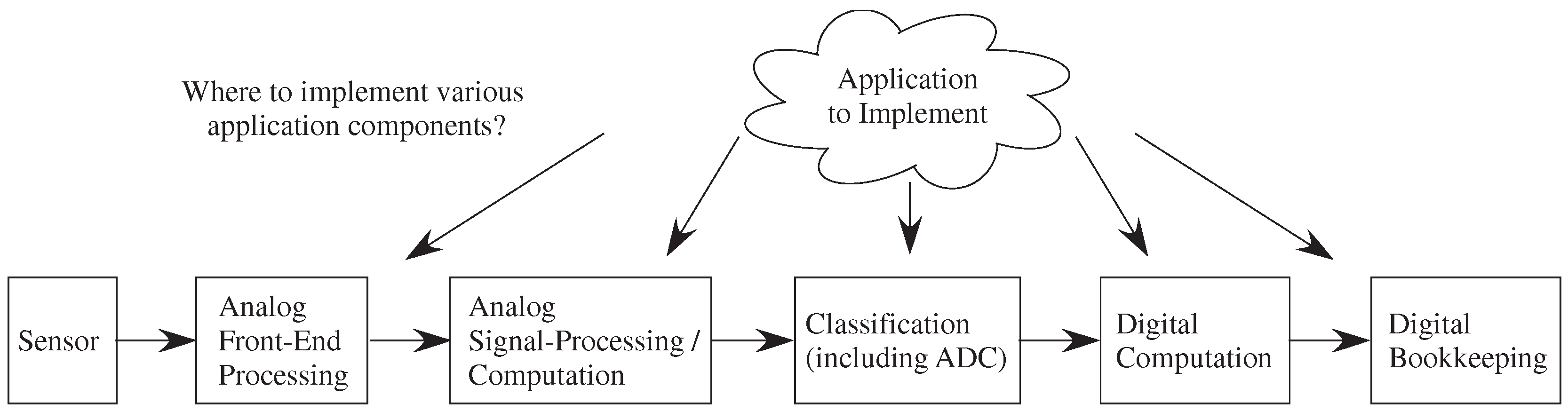
This new capability creates opportunities, but also creates design stress to address the resulting large co-design problem (Figure 7). The designer must choose the sensors as well as where to implement algorithms between the analog front-end, analog signal processing blocks, classification (mixed signal computation) which includes symbolic (e.g., digital) representations, digital computation blocks, and resulting μ P computation. Moving heavy processing to analog computation tends to have less impact on signal line and substrate coupling to neighboring elements compared to digital systems, an issue often affecting the integration of analog components with mostly digital computing systems. Often the line between digital and analog computation is blurred. For example, data-converters, or the more general case of analog classifiers, typically have digital outputs. The digital processor will be invaluable for bookkeeping functions, including interfacing, memory buffering, and related computations, as well as serial computations that are just better understood at the time of a particular design. Some heuristic concepts have been used previously, but far more research is required in building applications and the framework of these applications to enable co-design procedures in this space.
Analog computation directly implements dataflow parallelism. Analog executes as data appears. This representation allows parallel algorithms by design. Analog computation optimally merges data and computation, typical of data flow computation. The event data flow graphs fit well with neural computation/modeling, particularly for low average rate firing systems. Event (asynchronous) and clocked (synchronous) systems would be pipelined data flow systems [25]. The μ P primarily enables event driven processing as well as interfacing to outside synchronous digital world. Tool compilation will state whether enough resources are available, including computational components and data communication. The need for deep FIFOs, as in digital data flow implementations [24], is rarely needed except for final data logging and debugging.

4. System Level (Level = 1) versus Circuit Level (Level = 2) Design Environment

The structure of the Scilab/Xcos FPAA toolset was developed to enable both analog circuit design as well as system level design. The dataflow tool representation allows for a heterogenous mixture of courser-grain system concepts (Level = 1) as well as fine-grain circuit blocks (Level = 2). Figure 8 shows the considerations required for system (Level = 1) design. Definitions separating system level (Level = 1) and circuit level (Level = 2) started with an earlier FPAA structure [28], but only fully realized with the SoC FPAA structure [7]. Previous experience showed that circuit design was not compatible with system designer’s expectations of block diagrams (e.g., Simulink, Xcos); the definitions simplified the design process while not inhibiting either circuit-level or system-level design.

4.1. Level = 2: Enabling Circuit Designers to Build Level = 1 Blocks

Circuit level design (Level = 2) is straightforward for circuit designers, particularly analog designers. The goal of Level = 2 modeling would be to design, test, model, and build Level = 1 blocks that can be used by system designers. Each block represents a circuit element, either an element in the CAB (e.g., transistors, OTA) or a circuit block. Every line represents a single circuit connection providing current–voltage constraints. The tool directly compiles these elements into hardware, as well as simulates these circuits in Scilab/Xcos environment modeling the current-voltage relationships and interactions between blocks. The transistor simulation utilizes the analytic EKV model, only requiring six parameters for simulation; since we know the particular transistor of interest, whether it is 350 nm or 40 nm, and not every possible transistor dimension (e.g., W, L), this modeling is sufficient for these devices [29].
A Level = 2 block design is complete when encapsulated into a level = 1 model. The tools allows the user to graphically macroblock [30] CAB components into a block compiled into a single CAB. Every Level = 1 block uses a macromodel simulation for system simulation [7]. The model should closely correspond to experimental data, often encapsulating the characterization measurements and analysis performed to verify the block. Level = 2 blocks also utilize a tightly modeled macro modeled simulation for its circuit elements (e.g., OTA, FG OTA); the open availability of these models can assist designers in building their own Level = 1 models [29].
A designer Macromodeling circuit behavior enables the analog knowledge to be codified for future users and designers. The steps required in macro modeling are similar to the measurement and parameter fitting required for all successful designs. Macromodeling, starting from an op-amp model in 1974 [31], looks to create a nonlinear model to reproduce circuit responses as close as possible [32] using simpler digital numerical models. Models look to utilize generalized, low-order polynomials around a single fixed operating point [33,34,35,36,37], and some models utilize the nonlinear dynamics of the transistors [29,38,39,40]. These techniques often are coupled with tool design approach, particularly joint verification of digital and analog systems [41,42,43,44].
Our device models are derived to be generally applicable over a wide range of CMOS processes. The abstracted model parameters correspond to measured parameters from a group of SoC FPAA devices [6]. The abstracted model parameters are at a similar level to parameters published in technical papers that do not necessarily indicate any particular IC fabrication process details. Our devices were fabricated on a commercially available 350 nm CMOS process that one SoC FPAA was fabricated [6]. We would approach building models for other SoC FPAA devices along similar lines. One could directly use foundry data or SPICE simulations from foundry information to build these models, although that was not our approach. One taking this approach must be aware of inaccuracies in these models as well as understand the resulting IP restrictions resulting from a particular IC foundry. We expect extracted parameters at the similar level as published simulation data would be acceptable in these cases. Such cases could be valuable when investigating a new IC process when one does not have access to measured data.

4.2. Level = 1: Scilab/Xcos System Design Tools

System (Level = 1) design requires constraining the circuit representations just enough, and no further, for circuit design to directly fit into the data flow representation of Xcos environment. Level = 1 definitions are the minimum definitions required for circuit functionality (Figure 8) to align circuit concepts with Xcos dataflow approaches [24,25]. First, the blocks communicate using voltage signals, and the voltage signals must be abstracted to a single line (e.g., differential signals are represented by one line). Individual blocks can have internal current representations using voltage interfaces. Most blocks using current signals have internal voltage node(s) that can be communicated, so the constraint tends to have minimal issues. These constraints enable simpler and scalable ODE solutions instead of the nested current-voltage Level = 2 numerical ODE simulations. Standard single-ended digital design fits these definitions (e.g CMOS logic gates); the tools compile Verilog descriptions for compiled digital components. Second, lines represent a single or signal vector (signal bus), and each block must allow for the parallelization required for these signals.
Figure 9 shows representative Level = 1 blocks and their circuit representation. Each block represents core function, a more course-grain function [24], built out of FPAA components, that are not viewable in the tool. This practice is similar for digital computation, where few designs are developed at the level of logic gates or multiplication & addition, but rather most design in higher level algorithms (e.g., Cepstrum, Image Filtering, Classification) already encoded into libraries (e.g., MATLAB, Python). System level design should enable the user to build solutions without detailed knowledge of the underlying analog or mixed signal circuits, in the same way most users design digital algorithms without detailed knowledge of the underlying logic design. This abstraction provides a useful comparison between analog computations and digital computations.
Abstraction for graphical languages is necessary for efficient design, both for analog and digital languages. One application of hierarchical design is reducing on-screen complexity in graphical representations. Multilevel abstraction enables efficient graphical descriptions. If you try to graphically or in text keep everything together, it does not work. Deutsch limit can not have more than 50 visual primitives on the screen at the same time [45]. Multiple class projects using FPAA devices at Georgia Tech (e.g., [46,47]), as well as using related graphical tools like Labview for freshman robotics courses (e.g., ECE 1882), verify the need to keep the number of on-screen visual primitives smaller than 50; keeping the number of blocks below 25 seems important for debugging possibilities.
The few early attempts at analog synthesis in highly constrained spaces shows the hope of eventual analog synthesis (e.g. [48]). These systems attempt to do some initial macromodeling [49] and some symbolic representations [50] to eventually generate IC layout [51].
The definition of AMS languages (e.g., Verilog AMS, VHDL-AMS, Verilog-A), with some partial integration into IC design tools of Cadence [52] and Mentor Graphics [53], provide an alternate language framework to eventually implement the concepts we have described, but now in an IC design framework. The primary use of AMS languages is to rapidly include a new physical/analog component or circuit into some form of a SPICE model [54,55]. The AMS model tends to be to for transistor models (e.g., MOS EKV v2.6 [56]), for simple circuit components (e.g., [57] ), for specific abstracted linear system modeling (e.g., [58]), or for high level electrical models of mechanical systems to interface into electrical devices [59]. AMS is primarily a way to add devices into the Cadence analog simulation capabilities. These capabilities are extensions of voltage controlled current sources. Modelica and AMS languages have similar capabilities [60], where one can transfer between the two approaches with some optimization work. Given that Modelica, as part of Scilab/Xcos, is already available and utilized for our lowest level framework (Level = 2) in the tool flow, at a level at least equal to what is used in AMS languages, our approach shows what is possible with the potential of higher analog and mixed-signal abstraction.
Although an AMS language implementation could be utilized as the starting point for abstraction for analog IC design, considerable effort and infrastructure are required beyond the current state of these tools. Our techniques could be utilized with Cadence tools and to extend things if there is interest because our tools and techniques are open source. Although a language definition exists, the language has not been used, developed, etc to have any connection to real hardware or real synthesis. These tools are rarely used for developing frameworks, and when discussed, are entirely theoretical [61,62], effectively being too simple for practical implementations or not based in any physical implementation. These abstraction approaches highly constrains the system to simply analog pre- and post- processing, assuming simple linear system models [62,63]. One might find theoretical discussions of netlist partition strategies, important aspects for synthesis and abstraction, and yet separated from any analog circuit design concepts [64]. One sees a framework, but no synthesis or anything built. There is a strange sense that defining the language means something is built, but does not actually show abstraction; it just gives a framework to be illustrated [63]. AMS languages effectively are still only of limited interest, although models have been available for over 20 years.

5. Illustration of Complexity Available for Analog Abstraction

This section shows multiple examples demonstrating the design of many levels of analog/mixed-signal abstraction, showing the new capabilities and patterns in analog abstraction. The examples start with simple circuit elements and work towards analog computation, showing the complexity as well as abstraction throughout the process. FPAA abstraction, and resulting tool implementation, must involve compilation and simulation. These concepts introduce the abstraction of a complex circuit element, both in its suprising layers of required abstraction, as well as the amount of abstraction required for instrumenting the computation. Analog signal processing using these blocks requires a higher layer of abstraction, and computation, like classification and learning, requires even high layers of abstraction. These blocks show the large number of abstraction layers, and the constant reuse of components. The block abstraction concepts and tool design developed in an ethos of FPAA experimental design and measurement experience. Most of the application circuit implementations were not envisioned until after the SoC FPAA ICs were fabricated.
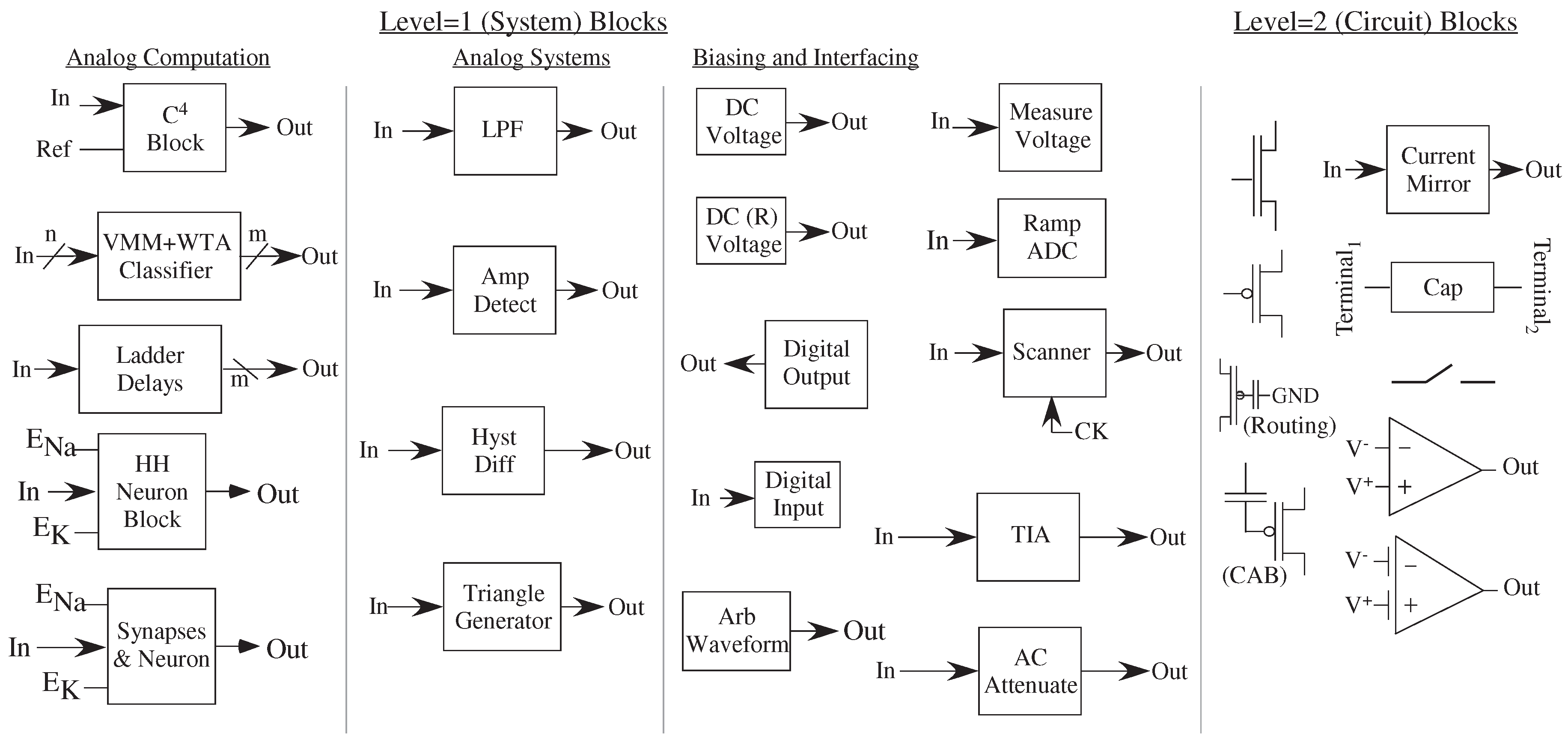
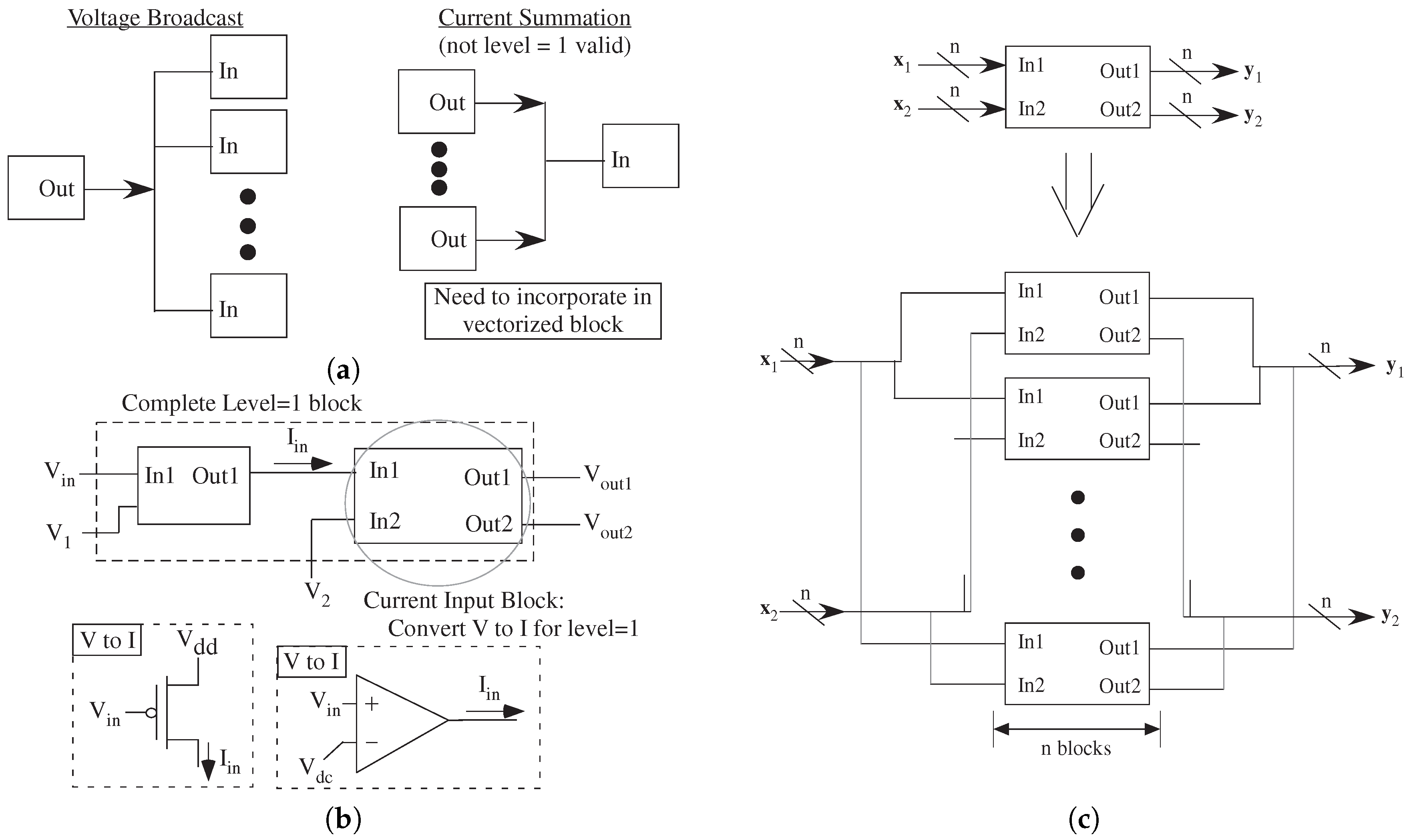
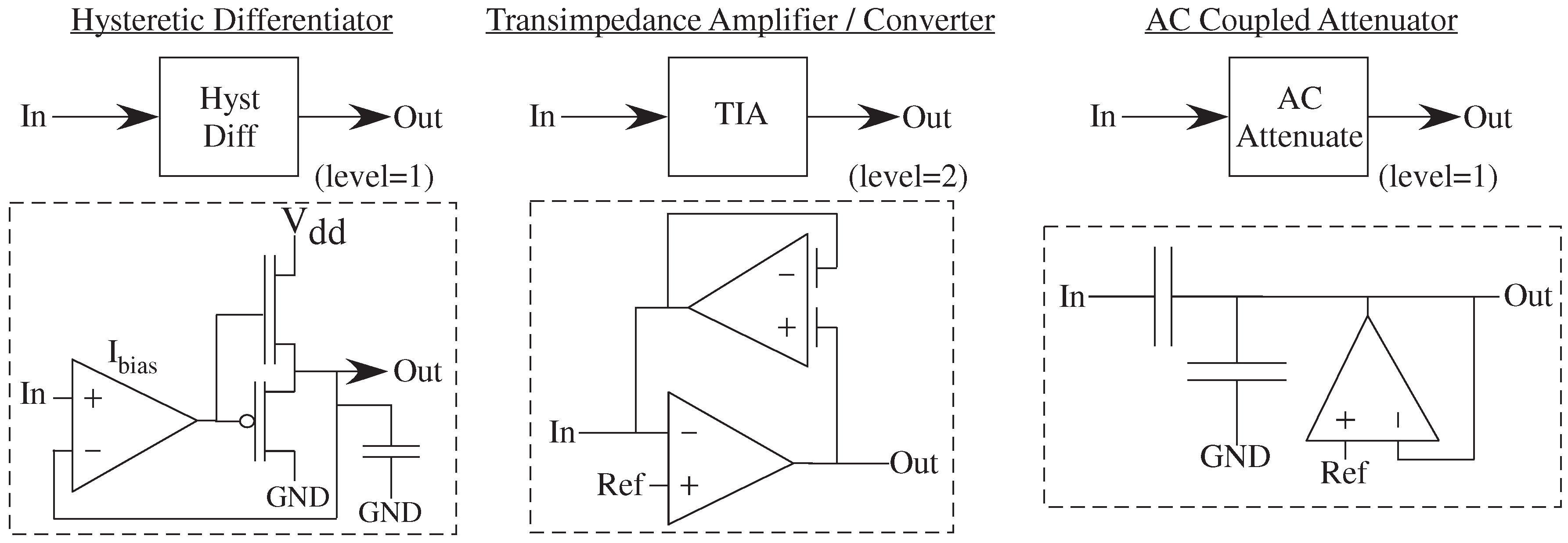
We have already seen a few representative Level = 1 blocks and their circuit representation (Figure 9). These blocks use a small number of components for input signal interfacing (AC Coupled Attenuator), for output signal interfacing (Transimpedance Amplifier), and for a range of linear and nonlinear (Hysteretic Differentiator) functions.
FG OTAs can be used for a number of applications required in analog circuit techniques. One can use these blocks to gain a signal between 10 and 100 around a DC value. Two OTA devices can build a divide by 10 or another value around a DC potential. Analog circuits often need to tune the particular input or output signal range between components. Two OTAs are be used to build the low-pass filter second-order section block definition (e.g., [65]). OTA blocks are important for building on music synthesis blocks [66], including the current block, CurrentStarvedInverter.
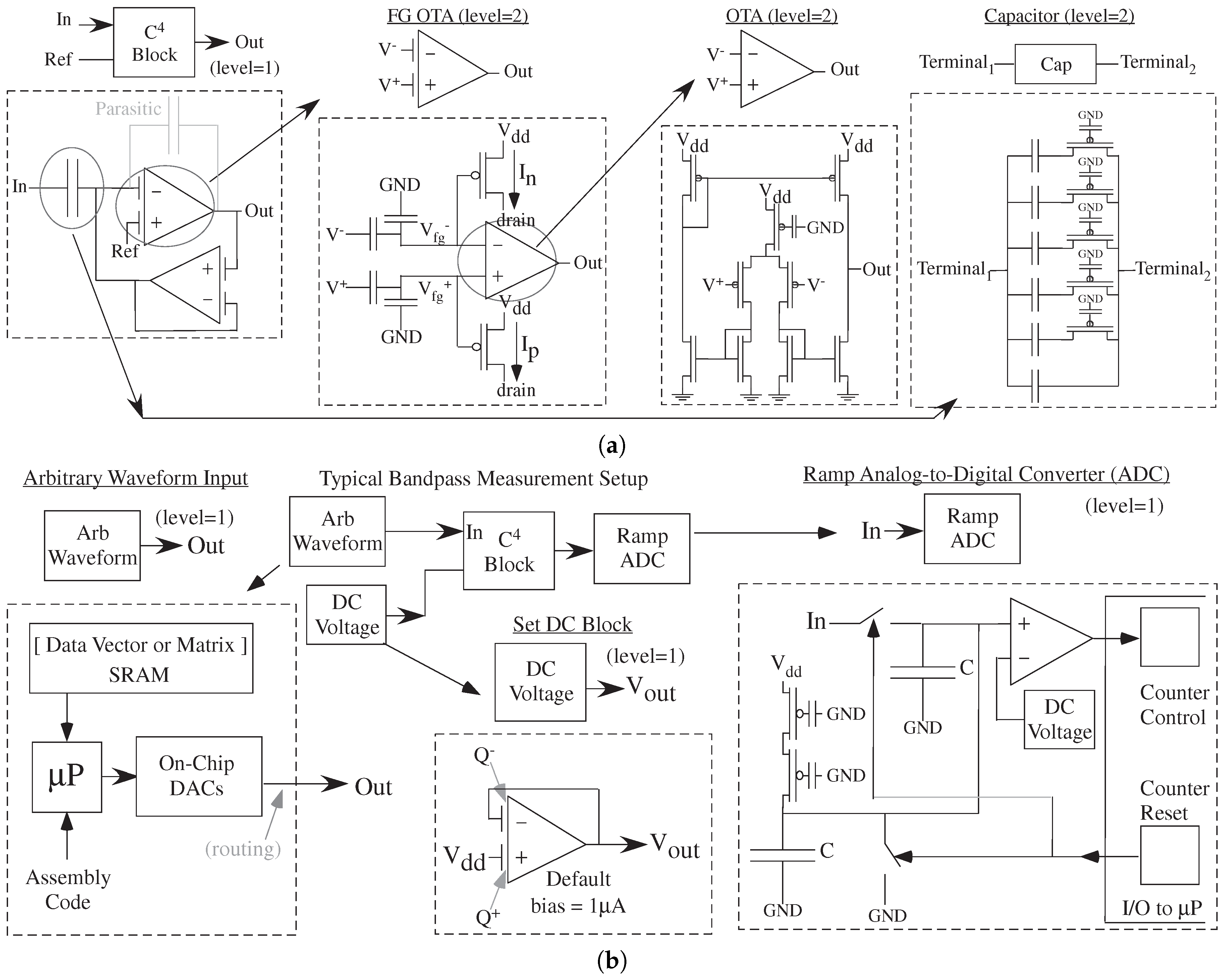
A simple second-order bandpass filter block (simulation and compilation) shows significant analog/mixed-signal abstraction (Figure 10), providing a useful example showing the number of levels of a few fundamental components required for reusable analog elements. The multiple levels of analog abstraction is significant in a typical implementation, levels that can be abstracted from the designer who only needs to use higher level blocks ( blocks in measurement setup of Figure 10b). The bandpass block, a G m -C C 4 bandpass filter topology, is deceptive because underlying the simple block are multiple levels of abstraction where FG elements are used throughout each structure, as well as tunable capacitor banks (Figure 10a). FG elements eliminate biasing issues through programable parameters; programmable parameters are essential for any abstractible physical system. FG enables abstraction by programmable components and abstraction makes users not unnecessarily focus on these details. IC designers want to see circuit details (Figure 10a), and are typically suprised at the detailed levels.
The blocks for testing require additional instrumentation blocks that are all part of the complete compiled system (Figure 10b). The set of blocks is the entire system. The blocks for instrumentation to test a component is part of the computation, illustrating the co-design trade-off in these areas. The DC voltage block is one FG OTA, set in unity gain configuration, and programmed with the required charge to set a DC voltage, eliminating the need for biasing structures (not tunable) or biasing DACs (large elements). The core structure looks like a highly sophisticated analog system design effectively built through a few blocks, simple and robust enough to be a user’s first day potential example. Typically, most analog/mixed-signal systems take a long time to build, and an even longer time to instrument. These techniques immediately show the issues and blocks to build, and eliminates the arbitrary (and unhelpful) lines between design and test.
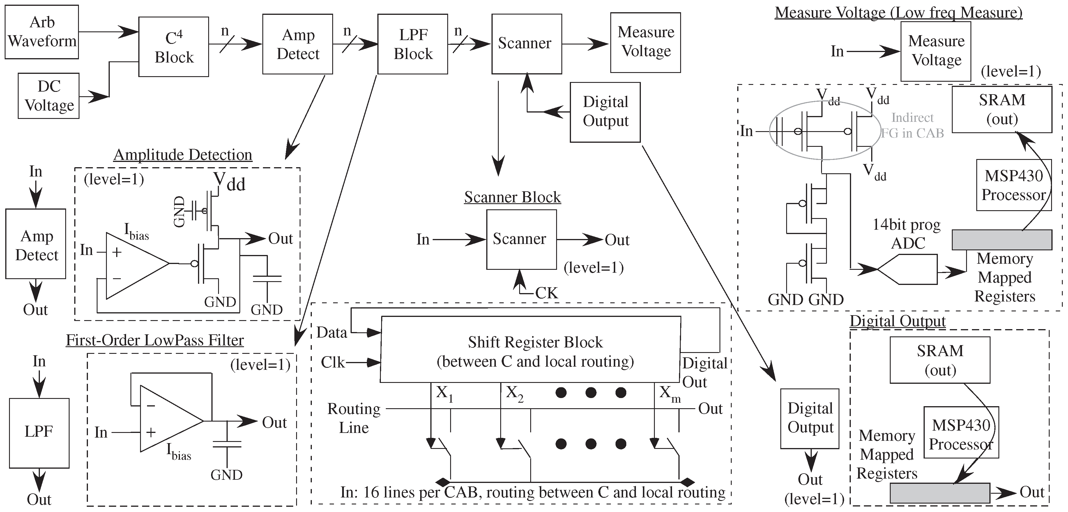
Moving to signal processing applications requires even higher levels of abstraction (Figure 11), particularly when considering computations like frequency decomposition (e.g., continuous-time wavelet transforms). The previous bandpass filters and amplitude detection block are key components for an exponentially scaled wavelet frequency decompostion (Figure 11). The computational chain requires a parallel bank of C 4 , a frequency decomposition, Amplitude Detection, or modulation to baseband, and an LPF. The core block fits into a single CAB and replicated for the number of required bands (Figure 11). Compiling a block into a single CAB results in a modular structure with minimal internal capacitance.
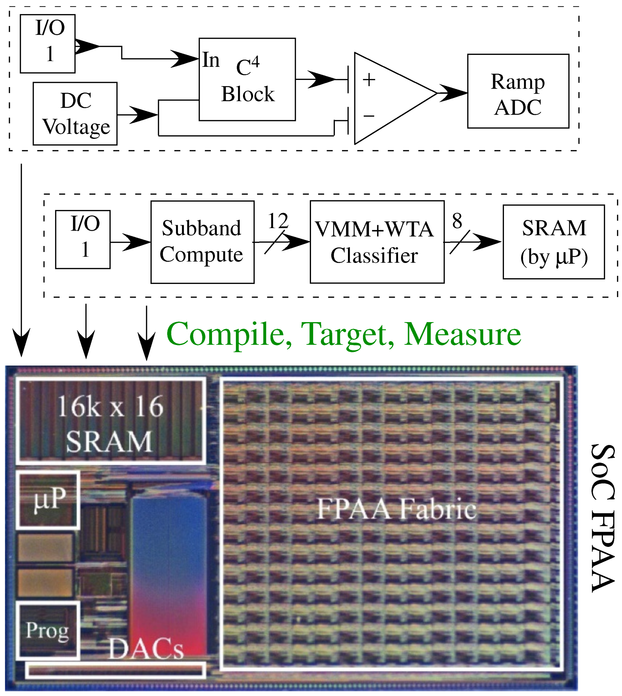
Table 1 summarizes representative available SoC FPAA interfacing blocks. The particular specifications directly affect the measurements possible for the resulting computation. This measurement illustrates the measure voltage block, effectively a slow speed (200SPS), high-resolution (14-bit) voltage measurement. The structure uses the FG programming circuitry, including the 14-bit measurement ramp ADC, still available in run mode. Measured data for this operation is shown in Figure 3 of [6]. The particular voltage measurement location can be multiplexed through the programming selection circuitry.
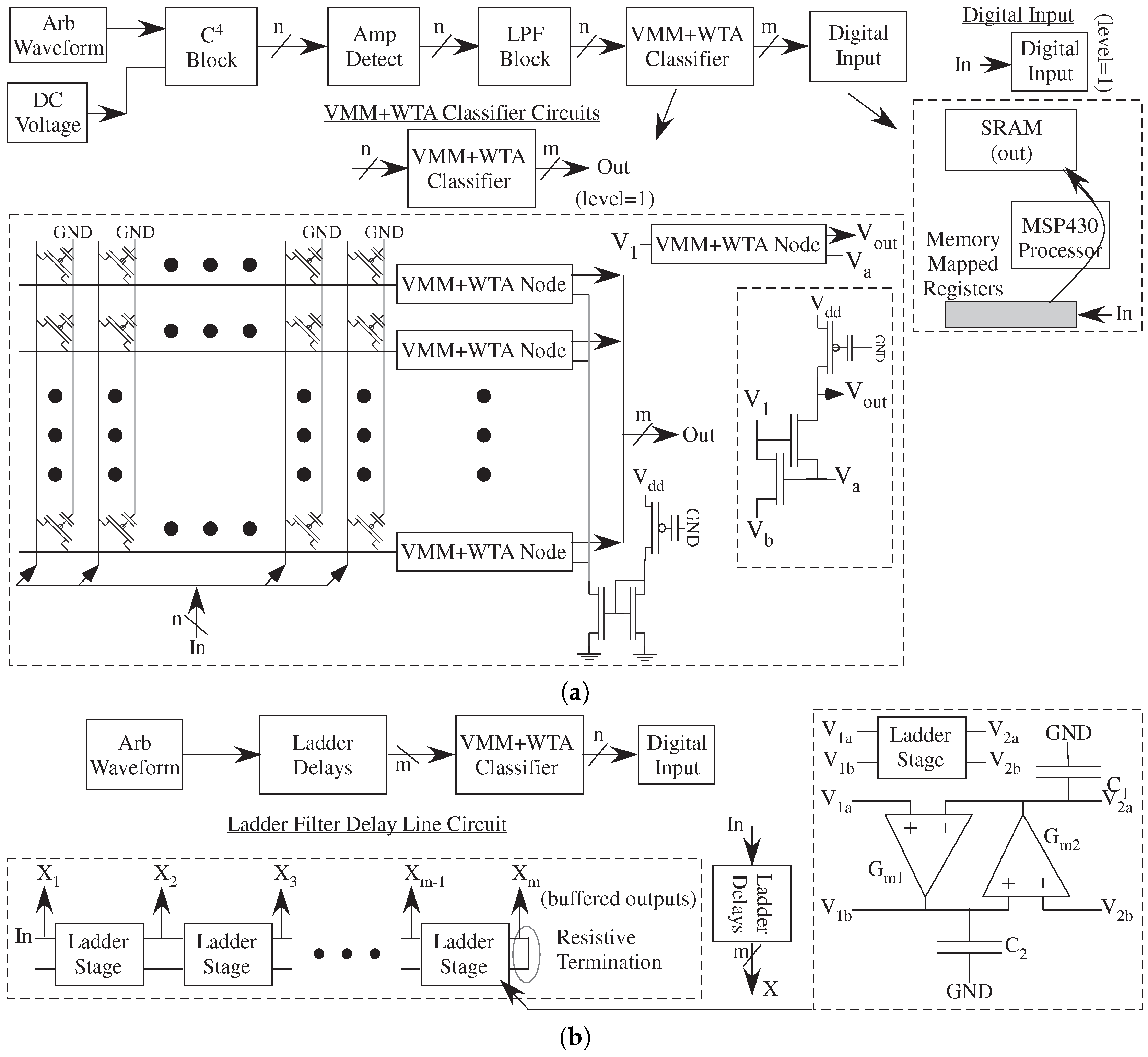
The step towards analog/mixed-signal computation, such as a classifier or learning classifier, requires more additional abstraction levels comprised of multiple modular components (Figure 12). Modular components are essential results for compiling these circuits into an FPAA structure. Six to either abstraction levels, typical of digital computation, are common for implementing this level of computation. These systems allow for sensors to classified symbolic data, a significant challenge for any system and interface design utilizing popular neural network accelerator hardware solutions. The front-end to the classifier stage could be chosen to the front-end frequency decomposition (Figure 11 abstracted into Figure 12a), or a continuous-time delay line approximation (Figure 12b). The choice of a front-end stage can be dependent on the signal classification algorithm as well as other nontechnical factors. The ladder filter basis function uses a number of coupled G m -C components with a similar complexity per output as the bandpass filter frequency decomposition.
Both approaches (Figure 12a,b) perform the final classification using a VMM+WTA classifier structure. The VMM items are FG local routing transistors. Unlike traditional FPGA architectures, which have optimized architectures for multipliers (and adds) and memory access to the computation, VMM in FG enabled FPAA devices is simply routing to the next computation with the non-volatile values locally stored. The structure used a digital input block to move the data from the circuit output into the μ P SRAM. Recent results show that this VMM+WTA classifier is capable of learning, utilizing additional analog circuit, interfacing, and μ P control (more assembly code), in a similar structure [67].
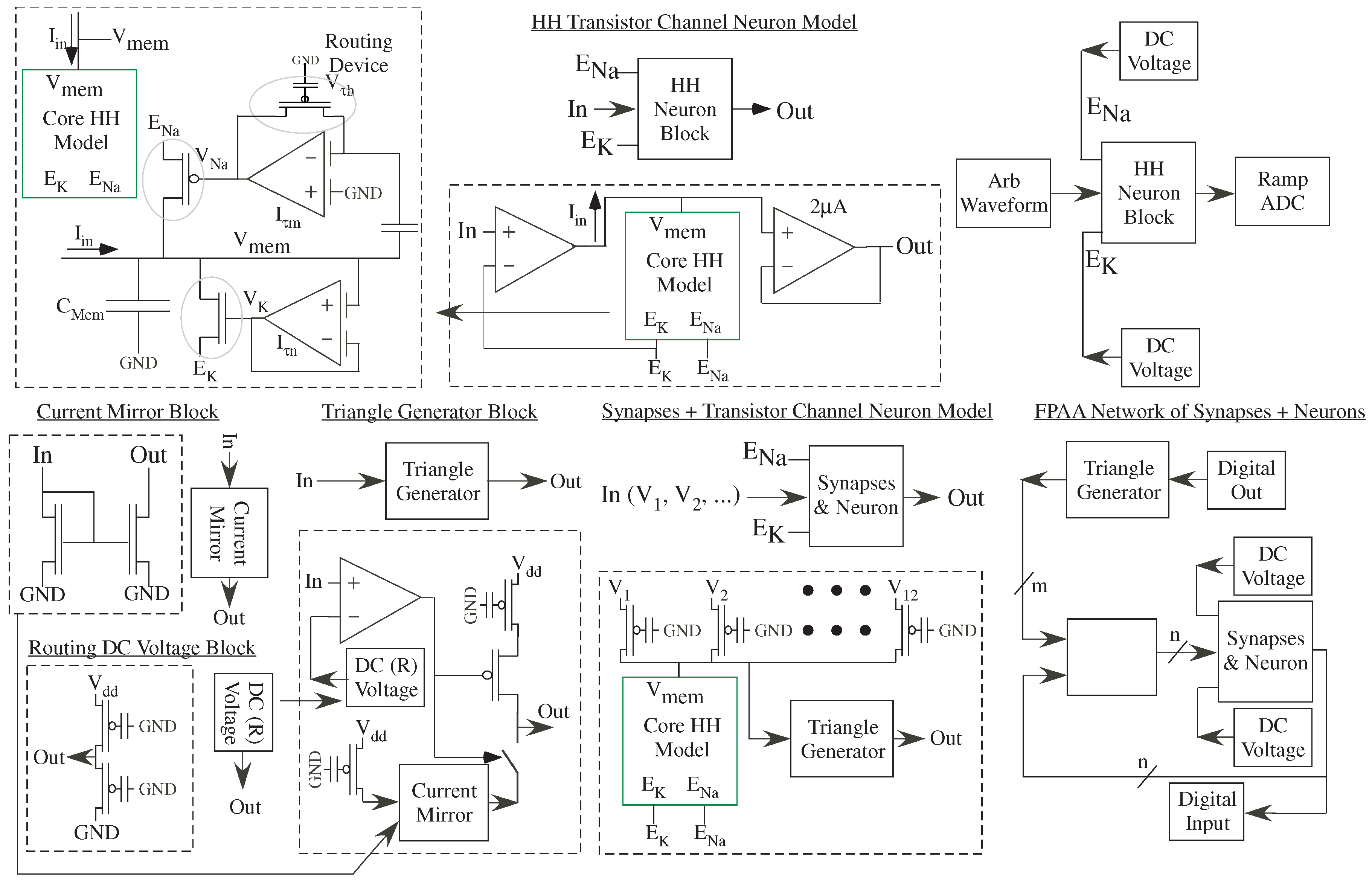
As another Classification and Learning example, abstraction techniques for analog classification can be extended to neuromorphically inspired approaches. The measurement structure shows a full layer of synaptically connected neurons, similar to the dynamics shown in custom ICs [68], with Level = 1 abstraction of neural blocks using the transistor channel model definitions (Figure 13). This block could specify the SoC FPAA [6] compilation of a network of 92 biologically modeled neurons each with 12–14 synaptic inputs and 10–12 network inputs. Learning techniques from the VMM + WTA classifier could be adapted for this network [67]. One could create a software interface to directly utilize the PyNN [69] neural representation for simulation or compilation. PyNN shows promise as a tool to unify multiple groups through an open community type tool used by multiple academics. The approach would extend to other neural network applications and approaches in a straightforward manner.
The core Hodgkin-Huxley (HH) model circuit (Level = 2) is an FPAA adaptation of the original channel neuron circuit [70]. Different applications result in different methods to supply the input current from input voltage(s) creating different blocks. For both cases, all components are chosen to embed the structure in a single CAB, macroblocking the design. One case uses an OTA to transform between voltage input to a single, direct current input into the neuron element(s). The membrane voltage (V m e n ) is buffered to the output. The measurement structure requires similar complexity to other circuits with an input, output, and two DC voltage biases (E k , E N a ) for all circuit instances. E K and E N A are the same biological supply for all neurons and therefore shared between blocks.
Synaptic elements to combine synaptic and neuron activity utilize the local routing FG transistors, adding another level of complexity that is abstracted through the high-level tool framework. The outputs are a triangle ramp that pre-computes the modeled charge concentration reaching the post-synaptic terminal. The number of synapses is limited, in this approach, by the number of local input routing lines. The inputs require a triangle ramp processing from their initial digital events. The ramp element can integrate directly on the line capacitance or can be buffered depending on the resulting synaptic current consumption. The routing DC Voltage block sets DC voltages using only routing fabric, using an FG pFET voltage follower, enabling dense setting of DC voltages. By characterizing one element, one gets a nearly ubiquitous voltage supply circuit that can be routed on any local line. Each CAB has local routing to Vdd and GND lines, so this component is always available with nearly no cost.

6. Collection of FPAA Blocks → Analog Computational Benchmarks

The FPAA block list (Figure 6) opens the discussion of fundamental block concepts of analog computational approaches. The current list of blocks in the Xcos/Scilab FPAA infrastructure (Figure 6) are fundamental circuits and blocks at two levels of depth (Level = 1 and 2). Table 2 summarizes the names of these blocks. Mead’s initial analog VLSI work already mentioned many of these core elements [65]. The addition of analog programmability and configurability enables both system level design as well as realistic systematic building up of these concepts. The block library shown allows for core analog circuit design through high-level applications, including acoustic, speech, and vision processing, as well as computation using networks of neurons which includes applications in optimal path planning.
Reuse of analog blocks (e.g., Figure 6) should reach a way similar to digital blocks, whether in custom circuits or in configurable (e.g., FPGA) platforms. Analog designers are known to be artistic in their craft and in the way they approach their craft. A master painter rarely reuses a part of another artist’s work, but rather the painter will add their artistic skill (e.g., optimizations) to the effort. Many companies (e.g., [71]) have tried to automate the analog design process, but failed because the solution was aimed for analog IC designers. A configurable analog/mixed-signal system-level platform, instead of relying on custom analog design, would create a demand for analog abstraction and automation. Abstracting analog design for system designers increases the chance of automation to be utilized. Reuse of analog blocks, similar to use in digital Verilog or C libraries, is both an opportunity for rapid growth of analog computing systems, as well as essential to the growth of the field. The FPAA system utilizes a number of blocks (Table 1 shows some representatives).
The blocks available give some insight on what we see for abstraction of analog functionality. The block library in Figure 6 is still a subset of blocks currently used. It would be hard to write down every digital algorithm, but both sets of computations usually arrive from a subset of fundamental primitives; specialized applications will always exist. Table 3 illustrates some of the resulting compiled FPAA computations, and some values of their resulting utilization on an SoC FPAA device. Related computations in telecommunications, such as VMM for beamforming and DCT computation, Viterbi and HMM classification, and computation of PDE solutions provide a fairly complete coverage of computations, particularly sensor computations. A computing approach based on large number of coupled ODEs [8] has tremendous potential. The capability for vectorized computations and representations enables system thinking. VMM is a fundamental operation in both analog and digital computation, providing a conceptual bridge between the approaches. Analog VMM implementation in routing fabric results in a huge advantage for analog computing opportunities.
The block library in Figure 6 is still a subset of blocks currently used because new blocks are being generated. Users of these tools have their own creative directions when solving application challenges, resulting in new innovations. These tools enable a similar case to a software library definition, enabling these capabilities for analog and mixed-signal design. The tools support these new innovations, and the authors encourage building up shared library spaces. An open FPAA infrastructure potentially fulfills the possibility of an open configurable architecture, unlike most commercial FPGA devices (e.g., [76,77]). A number of blocks are still not finished, and one expects a list is never completely finished. One expects eventually to have a complete set of ADC blocks, such as successive approximation, algoithmic, and pipeline architectures, a number of image processing blocks, communication circuits, and mixed signal computation such as distributed arithmatic linear phase computation [78].
Benchmark circuits are a way to codify what one means by computing. Defining an analog block library sets the stage to set up benchmarks circuits. The fundamental computation levels show potential parameterized set of benchmark circuits:
  • VMM + WTA acoustic classifier,
  • Neuron + moderate number of Synapses,
  • Analog filter with approximately linear phase constraints,
  • Biomedical signal regression and/or classification,
  • Image convolutions and/or classification,
  • Dendritic Classiciation,
  • Spatio-Temporal PDE solution, such as Path planning of a given network size.
A settled set of benchmark circuits enables both the characterization of existing configurable devices, as well as opening up research into optimal FPAA architectures. Analog benchmark circuits illustrates the meaning of computing.

7. Analog Abstraction: Summary and Implications

We see the first step in analog (and mixed signal) abstraction utilized in FPAA, encoded in the open-source SciLab/Xcos based toolset. The analog (and mixed signal) abstraction developed for the open-source toolkit used for the SoC FPAAs. Abstraction of Blocks in the FPAA block library makes the SoC FPAA ecosystem accessible to system-level designers while still enabling circuit designers the freedom to build at a low level. The test cases in the previous sections show various levels of complexity illustrating the analog abstraction capability. Abstract analog blocks, with digital components, into higher level abstractions enabled by the Scilab/Xcos toolset illuminates the higher-level representations for analog computation.
Although many aspects of analog abstraction are still yet to be discovered, they have hopefully shattered the view that analog devices, circuits, and systems are not abstractable. This abstraction is explicitly implemented in tools that enable CAD design, simulation, and compilable physical design. In no way have we made all of the blocks ever needed, but the framework is established to be evolved with new discoveries. Having any opportunity of a wide-scale utilization of ultra-low power technology both requires programmability/reconfigurability as well as abstractable tools. Abstraction is essential both make systems rapidly, as well as reduce the barrier for a number of users to use ultra-low power physical computing techniques.
In practice, two views are likely for analog computing, first, that analog device, circuits, and systems are just not abstractable like digital systems, and, second, that analog abstraction is incredibly difficult because one can not abstract analog functionality and computation in a similar way to digital computation. As mentioned earlier, sometimes macromodeling is used in larger analog projects to make simulation tractable and related uses, so some level of analog abstraction is considered by a few in the larger design community. Effectively, these two views are two sides of the same viewpoint since the effective perceived difference between these two viewpoints is between nearly impossible and not possible. This work challenges these viewpoints by explicitly demonstrating multiple layers of analog abstraction. These demonstrations lead to developing initial computing blocks libraries that compose a large number of analog signal processing and computation. Designing FPAA applications highly encourages creating reusable abstractable libraries.
The lowest level of analog abstraction occurs at a higher level than the lowest digital abstraction. Digital is built by simple operations, and yet it is constrained by these few operations—typically delays, arithmatic operations, and comparisons in a sampled time environment. Multiply-accumulate is a significant digital structure compared to a 1–10 transistor analog circuit. Analog circuits have a richer set of functions, starting from some common digital functions, as well as additional dynamic components (e.g., low-pass filters). Dataflow architectures become a useful framework for users to utilize these concepts. guiding the user’s intellectual framework, similar to early MATLAB guiding users towards developing vectorized code for higher performance.
Analog/mixed signal can have abstraction built similarly to digital computation, since there are no fundamental limitations of analog abstraction to digital abstraction. Some aspects will be more advantageous than others. Nothing fundamentally constrains analog approaches. Achieving these goals requires wide use of these techniques with a number of component libraries. Abstraction challenges center around developing a community of users developing various analog system level libraries. Growing a community requires effort and time, as well as resources to demonstrate a range of competitive applications. A commercial source of SoC FPAA devices would accelerate the development of these communities. As these libraries develop, code management techniques for the physical modules/routines will need to be developed. We expect that there will be specialized libraries where individuals require these techniques. A larger library helps refine the fundamental components while classifying particular blocks as needed. The abstraction is clear for the 100 s of digital standard cell library elements.
Analog/Mixed signal abstraction development could result in multiple new opportunities. Abstraction would potentially allow for topological optimization (e.g., Genetic Algorithms) to optimize a design for a particular application if appropriate system metrics can be described for the optimization. One can visualize extending these concepts outside of SoC FPAA compilation, or any FPAA compilation, to custom IC design approaches. One could extend the toolset from targeting FPAA devices to generating from the same high-level blocks, as either IC layout or the required files for IC layout, or directly generating IC layout. These correct by design concepts could open up translating FPAA solutions to custom IC solutions utilizing analog and digital standard cells, decreasing the transition cost between these solutions.

Author Contributions

J.H. developed the conceptualization, methodology, analysis, and writing of this paper. She was also involved in the investigation and validation of this effort. A.N. and S.K. primarily developed the software tools as well as were heavily involved in the validation of this work.

Acknowledgments

The authors wish to acknowledge the inspiration of this work’s effort resulted partially from our collaboration with Professor Florian Kolbl in Cergy, France, during the summer of 2017.

Conflicts of Interest

The authors declare no conflict of interest.

References

  1. Turing, R. On Computable Numbers. 1937. Available online: https://www.cs.virginia.edu/~robins/Turing_Paper_1936.pdf (accessed on 5 November 2018).
  2. Moore, G.E. Cramming more components onto integrated circuits. Electronics 1965, 38, 114–117. [Google Scholar] [CrossRef]
  3. Moore, G.E. Progress in Digital Integrated Electronics. IEEE IEDM 1975, 21, 11–23. [Google Scholar]
  4. Mead, C.; Conway, L. Introduction to VLSI System Design; Addison-Wesley: Boston, MA, USA, 1980; ISBN 0-201-24358-2. Available online: http://ai.eecs.umich.edu/people/conway/VLSI/VLSIText/VLSIText.html (accessed on 10 November 2018).
  5. Hasler, J. Opportunities in Physical Computing driven by Analog Realization. In Proceedings of the 2016 IEEE International Conference on Rebooting Computing (ICRC), San Deigo, CA, USA, 17–19 October 2016. [Google Scholar]
  6. George, S.; Kim, S.; Shah, S.; Hasler, J.; Collins, M.; Adil, F.; Wunderlich, R.; Nease, S.; Ramakrishnan, S. A Programmable and Configurable Mixed-Mode FPAA SoC. IEEE Trans. Very Large Scale Integr. (VLSI) Syst. 2016, 24, 2253–2261. [Google Scholar] [CrossRef]
  7. Collins, M.; Hasler, J.; George, S. An Open-Source Toolset Enabling Analog—Digital Software Codesign. J. Low Power Electron. Appl. 2016, 6, 3. [Google Scholar] [CrossRef]
  8. Hasler, J. Starting Framework for Analog Numerical Analysis for Energy Efficient Computing. J. Low Power Electron. Appl. 2017, 7, 17. [Google Scholar] [CrossRef]
  9. Mead, C. Neuromorphic electronic systems. Proc. IEEE 1990, 78, 1629–1636. [Google Scholar] [CrossRef] [Green Version]
  10. Hasler, J.; Marr, H.B. Finding a roadmap to achieve large neuromorphic hardware systems. Front. Neurosci. 2013, 7, 1–29. [Google Scholar] [CrossRef] [PubMed]
  11. Hall, T.; Twigg, C.; Gray, J.; Hasler, P.; Anderson, D. Large-scale Field-Programmable Analog Arrays for analog signal processing. IEEE Trans. Circuits Syst. I 2005, 52, 2298–2307. [Google Scholar] [CrossRef]
  12. Hasler, J.; Kim, S.; Adil, F. Scaling Floating-Gate Devices Predicting Behavior for Programmable and Configurable Circuits and Systems. J. Low Power Electron. Appl. 2016, 6, 13. [Google Scholar] [CrossRef]
  13. Twigg, C.M.; Gray, J.D.; Hasler, P. Programmable floating gate FPAA switches are not dead weight. In Proceedings of the IEEE International Symposium on Circuits and Systems, New Orleans, LA, USA, 27–30 May 2007; pp. 169–172. [Google Scholar]
  14. Schlottmann, C.; Hasler, P. A highly dense, low power, programmable analog vector-matrix multiplier: The FPAA implementation. IEEE J. Emerg. Sel. Top. Circuits Syst. 2011, 1, 403–411. [Google Scholar] [CrossRef]
  15. Peng, S.Y.; Gurun, G.; Twigg, C.M.; Qureshi, M.S.; Basu, A.; Brink, S.; Hasler, P.E.; Degertekin, F.L. A large-scale Reconfigurable Smart Sensory Chip. In Proceedings of the IEEE International Symposium on Circuits and Systems, Taipei, Taiwan, 24–27 May 2009; pp. 2145–2148. [Google Scholar]
  16. Ramakrishnan, S.; Wunderlich, R.; Hasler, J.; George, S. Neuron array with plastic synapses and programmable dendrites. IEEE Trans. Biomed. Circuits Syst. 2013, 7, 631–642. [Google Scholar] [CrossRef] [PubMed]
  17. Kim, S.; Shah, S.; Hasler, J. Calibration of Floating-Gate SoC FPAA System. IEEE Trans. Very Large Scale Integr. (VLSI) Syst. 2017, 25, 2649–2657. [Google Scholar] [CrossRef]
  18. Kim, S.; Hasler, J.; George, S. Integrated Floating-Gate Programming Environment for System-Level Ics. IEEE Trans. Very Large Scale Integr. (VLSI) Syst. 2016, 24, 2244–2252. [Google Scholar] [CrossRef]
  19. Hasler, J.; Shah, S. SoC FPAA Hardware Implementation of a VMM+WTA Embedded Learning Classifier. IEEE J. Emerg. Sel. Top. Circuits Syst. 2018, 8, 28–37. [Google Scholar]
  20. Hasler, J.; Wang, H. A Fine-Grain FPAA Fabric for RF+Baseband. In Proceedings of the GOMAC, Louis, MO, USA, 23–26 March 2015. [Google Scholar]
  21. Luu, J.; Goeders, J.; Wainberg, M.; Somerville, A.; Yu, T.; Nasartschuk, K.; Nasr, M.; Wang, S.; Liu, T.; Ahmed, N.; et al. VTR 7.0: Next Generation Architecture and CAD System for FPGAs. ACM Trans. Reconfigurable Technol. Syst. 2014, 7, 6. [Google Scholar] [CrossRef]
  22. Weis, T.; Knoll, M.; Ulbrich, A.; Muhl, G.; Brandle, A. Rapid Prototyping for Pervasive Applications. In Pervasive Computing; IEEE Computer Society: Washington, DC, USA, 2007; pp. 76–84. [Google Scholar]
  23. Boshernitsan, M.; Downes, M. Visual Programming Languages: A Survey; Report No. UCB/CSD-04–2368, EECS; University of California: Berkeley, CA, USA, 2004. [Google Scholar]
  24. Johnston, W.M.; Hanna, J.R.P.; Millar, R.J. Advances in Dataflow Programming Languages. ACM Comput. Surv. 2004, 36, 1–24. [Google Scholar] [CrossRef] [Green Version]
  25. Wadge, W.W.; Ashcroft, E.A. Lucid, The Dataflow Programming Language; Academia Press: Gent, Belgium, 1985. [Google Scholar]
  26. Evenchick, E. ICESTUDIO: An Open Source Graphical FPGA Tool. 2016. Available online: https://hackaday.com/2016/02/23/icestudio-an-open-source-graphical-fgpa-tool/ (accessed on 2 November 2018).
  27. Elliott, C.; Vijayakumar, V.; Zink, W.; Hansen, R. National Instruments LabVIEW: A Programming Environment for Laboratory Automation and Measurement. J. Assoc. Lab. Autom. 2007, 12, 17–24. [Google Scholar] [CrossRef]
  28. Schlottmann, C.; Hasler, J. High-level modeling of analog computational elements for signal processing applications. IEEE Trans. Very Large Scale Integr. (VLSI) Syst. 2014, 22, 1945–1953. [Google Scholar] [CrossRef]
  29. Natarajan, A.; Hasler, J. Modeling, simulation and implementation of circuit elements in an open-source tool set on the FPAA. Analog Integr. Circiuits Signal Process. 2017, 91, 119–230. [Google Scholar] [CrossRef]
  30. Kim, S.; Shah, S.; Wunderlich, R.; Hasler, J. CAD Synthesis Tools for Large-Scale Floating-Gate FPAA System. J. DAES 2017. submitted. [Google Scholar]
  31. Boyle, G.R.; Cohn, B.M.; Pederson, D.O.; Solomon, J.E. Macromodeling of Integrated Circuit Operational Amplifier. IEEE J. Solid-State Circuits 1974, SC-9, 353–363. [Google Scholar] [CrossRef]
  32. Casinovi, G. A macromodeling algorithm for analog circuits. IEEE Trans. Comput.-Aided Des. Integr. Circuits Syst. 1991, 10, 150–260. [Google Scholar] [CrossRef]
  33. Batra, R.; Li, P.; Pileggi, L.T.; Chien, Y. A methodology for analog circuit macromodeling. In Proceedings of the 2004 IEEE International Behavioral Modeling and Simulation Conference, San Jose, CA, USA, 22 October 2004. [Google Scholar]
  34. Wang, J.; Li, X.; Pileggi, L.T. Parameterized macromodeling for analog system-level design exploration. In Proceedings of the 44th Annual Design Automation Conference, San Diego, CA, USA, 4–8 June 2007; pp. 940–943. [Google Scholar]
  35. Wei, Y.; Doboli, A. Structural macromodeling of analog circuits through model decoupling and transformation. IEEE Trans. CAD 2008, 27, 712–725. [Google Scholar] [CrossRef]
  36. Wei, Y.; Doboli, A. Systematic development of analog circuit structural macromodels through behavioral model decoupling. In Proceedings of the 42nd Annual Design Automation Conference, Anaheim, CA, USA, 13–17 June 2005; pp. 57–62. [Google Scholar]
  37. Ding, M.; Vemuri, R. A two-level modeling approach to analog circuit performance macromodeling. In Proceedings of the IEEE DATE in Europe, Munich, Germany, 7–11 March 2005; pp. 1530–2531. [Google Scholar]
  38. Odame, K.; Hasler, P. A bandpass filter with inherent gain adaptation for hearing applications. IEEE Trans. Circuits Syst. I 2008, 55, 786–795. [Google Scholar] [CrossRef]
  39. Odame, K.; Hasler, P. Theory and Design of OTA-C Oscillators with Native Amplitude Limiting. IEEE Trans. Circuits Syst. I 2009, 56, 40–50. [Google Scholar] [CrossRef]
  40. Odame, K.; Hasler, P.E. Nonlinear Circuit Analysis via Perturbation Methods and Hardware Prototyping. VLSI Des. 2010, 2010, 687498. [Google Scholar] [CrossRef]
  41. Lim, B.C.; Mao, J.; Horowitz, M.; Jang, J.; Kim, J. Digital analog design: Enabling mixed-signal system validation. IEEE Des. Test 2015, 32, 44–52. [Google Scholar] [CrossRef]
  42. Kim, J.; Jerradit, M.; Lim, B.; Horowitz, M. Leveraging designer’s intent: A path toward simpler analog CAD tools. In Proceedings of the IEEE CICC, Rome, Italy, 13–16 September 2009; pp. 613–620. [Google Scholar]
  43. Liao, S.; Horowitz, M. A verilog piecewise-linear analog behavior model for mixed-signal validation. IEEE Trans. Circuits Syst. I 2014, 61, 2229–2235. [Google Scholar] [CrossRef]
  44. Lim, B.C.; Horowitz, M. Error control and limit cycle elimination in event-driven piecewise linear analog functional models. IEEE Trans. Circuits Syst. I 2016, 63, 23. [Google Scholar] [CrossRef]
  45. Sempere, A. Animatronics, Children and Computation. J. Educ. Technol. Soc. 2005, 8, 11–21. [Google Scholar]
  46. Twigg, C.; Hasler, P. Incorporating Large-Scale FPAAs into Analog Design and Test Courses. IEEE Trans. Educ. 2008, 51, 319–324. [Google Scholar] [CrossRef]
  47. Hasler, J.; Kim, S.; Shah, S.; Adil, F.; Collins, M.; Koziol, S.; Nease, S. Transforming mixed-signal circuits class through SoC, FPAA IC, PCB, and toolset. In Proceedings of the European Workshop on Microelectronics Education (EWME), Southampton, NY, USA, 11–13 May 2016; pp. 1–2. [Google Scholar]
  48. Donnay, S.; Gielen, G.; Sansen, W.; Kruiskamp, W.; Leenaarts, D.; Bokhoven, W. High-level synthesis of analog sensor interface front-ends. In Proceedings of the 1997 European conference on Design and Test, Paris, France, 17–20 March 1997; pp. 56–60. [Google Scholar]
  49. Vandenbussche, J.; Donnay, S.; Leyn, F.; Gielen, G.; Sansen, W. Hierarchical top-down design of analog sensor interfaces: From system-level specifications down to silicon. In Proceedings of the DATE ’98 Design, Automation and Test in Europe, Paris, France, 23–26 February 1998. [Google Scholar]
  50. McConaghy, T.; Eeckelaert, T.; Gielen, G. CAFFEINE: Template-Free Symbolic Model Generation of Analog Circuits via Canonical Form Functions and Genetic Programming. In Proceedings of the DATE ’05 Design, Automation and Test in Europe, Munich, Germany, 7–11 March 2005. [Google Scholar] [Green Version]
  51. Donnay, S.; Swings, K.; Gielen, G.; Sansen, W. A methodology for analog high-level synthesis. In Proceedings of the IEEE Custom Integrated Circuits Conference, San Diego, CA, USA, 1–4 May 1994; pp. 373–376. [Google Scholar]
  52. Cadence Verilog-AMS Language Reference. Available online: http://www2.ece.ohio-state.edu/~bibyk/ece822/verilogamsref.pdf (accessed on 10 November 2018).
  53. Cooper, S. System Modeling: An Introduction. November 2007. Available online: www.mentor.com/systemvision (accessed on 21 October 2018).
  54. Nagel, L.W.; Pederson, D.O. SPICE (Simulation Program with Integrated Circuit Emphasis); Memorandum No. ERL-M382; University of California: Berkeley, CA, USA, 1973. [Google Scholar]
  55. Quarles, T.L. Analysis of Performance and Convergence Issues for Circuit Simulation; Memorandum No. UCB/ERL M89/42; University of California: Berkeley, CA, USA, 1989. [Google Scholar]
  56. Lallement, C.; Pecheux, F.; Vachoux, A.; Pregaldiny, F. Compact modeling of the MOSFET in VHDL-AMS. In Transistor Level Modeling for Analog/RF IC Design; Springer: Cham, The Netherlands, 2006. [Google Scholar]
  57. Wang, W.; Carter, H.; Yan, J. A high-level VHDL-AMS model design methodology for analog RF LNA and mixer. In Proceedings of the IEEE Behavioral Modeling and Simulation Conference, San Jose, CA, USA, 21–22 October 2004. [Google Scholar]
  58. Pandit, S.; Mandal, C.; Patra, A. A Formal Approach for High Level Synthesis of Linear Analog Systems. In Proceedings of the GLVLSI, Philadelphia, PA, USA, 30 April–1 May 2006; pp. 345–348. [Google Scholar]
  59. Pecheux, F.; Lallement, C.; Vachoux, A. VHDL-AMS and Verilog-AMS as Alternative Hardware Description Languages for Efficient Modeling of Multi-Discipline Systems. IEEE Trans. Comput.-Aided Des. Integr. Circuits Syst. 2003, 24, 204–225. [Google Scholar] [CrossRef]
  60. Enge-Rosenblatt, O.; Haase, J.; Claus, C. Important characteristics of VHDL-AMS and modelica with respect to model exchange. In Proceedings of the Workshop on Equation-Based Object-Oriented Languages and Tools, Berlin, Germany, 30–31 July 2007; pp. 28–89. [Google Scholar]
  61. Antao, B.A.A.; Brodersen, A.J. A framework for synthesis and verification of analog systems. Analog Integr. Circuits Signal Process. 1995, 8, 183–299. [Google Scholar] [CrossRef]
  62. Antao, B.A.A.; Brodersen, A.J. ARCHGEN: Automated Synthesis of Analog Systems. IEEE Trans. Very Large Scale Integr. 1995, 3, 231–244. [Google Scholar] [CrossRef]
  63. Haase, J. Rules for analog and mixed-signal VHDL-AMS modeling. In Languages for System Specification; Kluwer Academic Publishers: Norwell, MA, USA, 2005; pp. 169–282. [Google Scholar]
  64. Shields, J.; Christen, E. Mixed nets, conversion models, and VHDL-AMS. In Advances in Design and Specification Languages for SoCs; Boulet, P., Ed.; Springer: Berlin, Germany, 2005; Chapter 2; pp. 21–29. [Google Scholar]
  65. Mead, C. Analog VLSI and Neural Systems; Addison Wesley: Boston, MA, USA, 1989. [Google Scholar]
  66. Nease, S.H.; Lanterman, A.D.; Hasler, J.O. Applications of Current-Starved Inverters to Music Synthesis on Field-Programmable Analog Arrays. J. Audio Eng. Soc. 2018, 66, 71–79. [Google Scholar] [CrossRef]
  67. Hasler, J.; Shah, S. Learning for VMM+WTA Embedded Classifiers; Georgia Institute of Technology: Orlando, FL, USA, 2016. [Google Scholar]
  68. Brink, S.; Nease, S.; Hasler, P.; Ramakrishnan, S.; Wunderlich, R.; Basu, A.; Degnan, B. A learning-enabled neuron array IC based upon transistor channel models of biological phenomena. IEEE Trans. Biomed. Circuits Syst. 2013, 7, 71–81. [Google Scholar] [CrossRef] [PubMed]
  69. Davison, A.P.; Broderle, D.; Eppler, J.M.; Kremkow, J.; Muller, E.; Pecevski, D.A.; Perrinet, L.; Yger, P. PyNN: A common interface for neuronal network simulators. Front. Neuroinform. 2009, 2, 11. [Google Scholar] [CrossRef] [PubMed]
  70. Farquhar, E.; Hasler, P. A bio-physically inspired silicon neuron. IEEE Trans. Circuits Syst. I 2005, 52, 477–488. [Google Scholar] [CrossRef]
  71. Barcelona Design. Available online: http://www.barcelonadesign.com (accessed on 15 July 2017).
  72. Natarajan, A.; Hasler, J. Neuron paper Hodgkin Huxley Neuron and dynamics on the FPAA. Trans. Biol. Circuits Syst. 2018. submitted. [Google Scholar]
  73. Shah, S.; Hasler, J. Tuning of Multiple Parameters with a BIST System. IEEE Circuits Syst. I 2017, 64, 1772–1780. [Google Scholar] [CrossRef]
  74. Shah, S.; Hasler, J. Low Power Speech Detector On A FPAA. In Proceedings of the 2017 IEEE International Symposium on Circuits and Systems (ISCAS), Baltimore, MD, USA, 28–31 May 2017. [Google Scholar]
  75. Shah, S.; Hasler, J. VMM + WTA Embedded Classifiers Learning Algorithm implementable on SoC FPAA devices. IEEE J. Emerg. Sel. Top. Circuits Syst. 2018, 8, 65–76. [Google Scholar]
  76. Wawrzynek, J. Should the academic community launch an open-source FPGA device and tools effort? In Proceedings of the ACM/SIGDA FPGA, Monterey, CA, USA, 22–24 February 2011; pp. 2–3. [Google Scholar]
  77. Liu, H.J. Archipelago—An Open Source FPGA with Toolflow Support; Technical Report No. UCB/EECS-2014–23; University of California: Berkeley, CA, USA, 2014. [Google Scholar]
  78. Ozalevli, E.; Huang, W.; Hasler, P.E.; Anderson, D.V. A reconfigurable mixed-signal VLSI implementation of distributed arithmetic used for finite impulse response filtering. IEEE Trans. Circuits Syst. I 2008, 55, 510–521. [Google Scholar] [CrossRef]
Figure 1. Analog Abstraction into fundamental blocks enables implementation into configurable systems, similar to digital counterparts. Analog (or mixed-signal) circuits, such as a classical sensor system with a variable gain amplifier (top), or analog computation, such as an acoustic word classifier (second), are built from a common high-level approach. This discussion is beyond a theoretical discussion because of the existence of configurable devices, such as the SoC large-scale Field Programmable Analog Array (FPAA, die photo shown).
Jlpea 08 00047 g001
Figure 2. Digital Computation builds from Turing Machines as the foundation for computer architectures, computer algorithms, and resulting numerical analysis. All digital computing devices are based on this framework. Although traditional analog computation has little computational framework, recent opportunities in configurable implementation of analog/mixed-signal computation has created interest as well as initial results towards building these systematic design approaches, This effort considers analog and mixed signal abstraction centered around the tool efforts required for system-level FPAA design. These techniques are only the beginning of these directions.
Jlpea 08 00047 g002
Figure 3. Comparison of Cloud computation, on-device computation, and FPAA computation. For cloud computation and for on-device computation, we only consider the energy required for communication. All devices might have an RF radio; we consider just the part required for this core computation. For FPAA computation, we include the entire device. If cloud computation were considered free, then cloud and on-device computation would appear to be of similar complexity. FPAA computation dramatically decreases the resulting on-device computation.
Jlpea 08 00047 g003
Figure 4. SoC FPAA approach consists of key innovations in FPAA hardware, innovations and developments in FPAA tool structure as well as innovations in the bridges between them. One typically focuses on what circuit and system applications can be built on the FPAA platform, but every solution is built up for a large number of components ideally abstracted away from the user.
Jlpea 08 00047 g004
Figure 5. RASP 3.0 functional block diagram illustrating the resulting computational blocks and resulting routing architecture. The infrastructure control includes a microprocessor ( μ P) developed from an open-source MSP430 processor, as well as on chip structures include the on-chip DACs, current-to-voltage conversion, and voltage measurement, to program each Floating-Gate (FG) device. The FG switches in the Connection (C) Blocks, the Switch (S) Blocks, and the local routing are a single pFET FG transistor programmed to be a closed switch over the entire fabric signal swing of 0 to 2.5 V. Eight, four-input Boolean Logic Element (BLE) lookup tables with a latch comprise the CLB blocks. Transconductance amplifiers, transistors, capacitors, switches, as well as other elements comprise the CAB blocks. (Adapted from Figure 2 in [6]).
Jlpea 08 00047 g005
Figure 6. Illustration of several existing FPAA blocks, both level 1 and 2, for infrastructure and computation. Level = 2 blocks tend to correspond to CAB (Computational Analog Block) elements in the FPAA. Not all blocks are shown, but representative samples; the list will grow with further innovations.
Jlpea 08 00047 g006
Figure 7. Enabling programmable and configurable computation from the sensors to the final stored digital results in a huge co-design problem. Unlike the typical co-design concerns between partitioning code between digital computation (e.g., FPGAs) and μ P, this discussion has potentially five layers of heterogeneous opportunities requiring informed decisions for near optimal designs in a finite amount of time.
Jlpea 08 00047 g007
Figure 8. Illustration of Level = 1 requirements. These requirements enable level = 1 solutions to fit a typical graphical dataflow system, as one would expect in Simulink or Xcos. (a) level = 1 requires that block inputs and outputs are voltages, enabling voltage broadcast, and eliminating difficulties with current summation for the tool; (b) a current input (or output) must have another block that converts the signal representation, in a linear or nonlinear manner, to voltage inputs (or output). Common transformations from input voltage to output current include MOSFET transistors or Transconductance Amplifiers (TA), both frequently available on-chip; (c) all signals to the blocks must be vectorized to represent input data buses (n signals), not just individual signals. This requires that block definitions, both in simulation and in hardware targeting, must enable parallelized representations (e.g., n blocks).
Jlpea 08 00047 g008
Figure 9. Example FPAA blocks following Level = 1 definitions. Hysteretic Differentiator block uses nonlineary dynamics to find zero crossings, minimum and maximum signal values. Transimpedance Amplifier (/converter) enables current output circuits to be represented at Level = 1 blocks, such as in VMM computation. The circuit also is important for sensor interfacing applications. An AC coupled attenuator allows for precise level-shifted small signals to be applied to a circuit; selecting the input capacitor affects the input attenuation. Voltage can be amplified using the open loop FG OTA block in Figure 1, where the gain (e.g., 10–50) is chosen by coupling capacitors.
Jlpea 08 00047 g009
Figure 10. Analog Abstraction, abstracted from the typical user, has multiple levels of depth. The measuring a bandpass block illustrate these levels of complexity (the Capacitively Coupled Current Conveyer, or C 4 , G m -C, device). (a) components in the C 4 bandpass filter block. This block is directly parallelizable, so one element is shown for clarity. The filter requires two FG OTAs and one capacitor, corresponding to CAB (Level = 2) elements. The capacitor block allows for scaling the number of capacitors with six equal sized devices. The FG OTA is a dedicated component using selectable capacitive inputs to a regular OTA device found in the CAB elements. The floating-gate charge can be programmed through measurements of I n and I p and abstracted through the tool. The OTA device uses an FG bias current source for a typical 9-transistor OTA topology [65]; (b) typical setup for end-to-end use (experimental measurements) of the bandpass filter block. The blocks for testing show additional instrumentation blocks that are all part of the complete compiled system. The DC Voltage block uses an FG OTA device, configured for unity-gain, programmed (modifying Q + and Q ) for a particular voltage output. The Arbitrary waveform block uses the digital μ P to supply signals on a DAC, routed to the desired input block. The Ramp ADC block also uses μ P control to build a converter from an OTA, T-gate switches (CAB elements), and FG elements available in routing.
Jlpea 08 00047 g010
Figure 11. Tool blocks for acoustic subband computation: bandpass filter bank, amplitude detection, and time window filtering for later processing. Measuring this block introduces the amplitude detection and first-order LPF blocks, both requiring one OTA each. These three elements make up an subband compute block (Figure 1). The structure requires the scanner block, targeted as a set of T-gate switches and shift register in routing between the CABs and C block routing, to multiplex the multiple signals. The scanner is controlled by digital output block taking μ P signals into the CAB. The measure voltage block, a low-frequency (200SPS) block utilizing the 14-bit ramp ADC in the programming infrastructure [18] to connect with the digital system. The approximate gain from In through the ADC is nearly 1 and calibrated on-chip [17].
Jlpea 08 00047 g011
Figure 12. Compilation of classification architectures with full end-to-end sensor to classified data in simple graphical code definitions. (a) signal processing and classification block chain with n input and m output VMM + WTA classifier block. The chain uses a digital input block to get the results from the VMM + WTA classifier; (b) implementation of a classifier network using an approximate delay line. This approximate delay line is an example of a ladder filter network, a G m -C realization of a prototypical LC delay line; other LC filters and PDE approximations (wave guiding networks) would utilize this framework.
Jlpea 08 00047 g012
Figure 13. Blocks based on transistor channel model for neurobiological systems, enabling compilable networks of neurons and synapses. From one core HH model circuit, one can develop a set of parallel neuron blocks, as well as a set of parallel neuron and synapse block in the FPAA fabric. FG switch elements model the programmable synapse elements. Triangle Generator Block creates the presynaptic waveforms required for biological synapse response. The DC voltage block in Routing (R) uses two routing elements, nominally in a voltage follower configuration, to enable a programmed voltage source on any local CAB routing line (and can be routed into the fabric). The nFET current mirror block (Level = 2) corresponds to the nFET current mirror available in the CABs.
Jlpea 08 00047 g013
Table 1. Summary of representative SoC FPAA interfacing blocks.
Summary of Typical Input Devices for the SoC FPAA Structures (20 MHz Clock)
NameTypeBitsRateRange
DCVoltageCompiled Analog Circuit≈14DC-200SPS0–2.5 V
DC_voltage μ P controlled DAC7 0–2.5 V (or 0.2–2.1 V)
ARB Gen μ P controlled DAC7 a p p r o x 1 MSPS0–2.5 V
GPIO_in μ P controlled GPIO16 (bus)10 MSPS0–2.5 V
Summary of Typical Output Devices for the SoC FPAA Structures
NameTypeBitsRateRange
meas_volt (ADC)ramp + FG input14200 SPS0–2.5 V (or 0.1 to 2.4 V)
ADC1/2 2IP block8kSPS0–2.5 V
Ramp_ADCramp8kSPS0.1–2.4 V
Table 2. Summary of important Level = 1 and Level = 2 blocks that include the complete block attributes of compilation, simulation, and documentation.
Computation (Level 1)Signal Processing (Level 1)Instrumentation (Level 1)Components (Level 2)
vmmwtalpfOTARAMP_ADCnfet
SubbandArrayHyst_diffDC Voltagepfet
LadderFilterMin_detectDigital InputFG_pfet
hhneuronMax_detectDigital OutputMITE
InfNeuronOTA_bufArb Waveformnmirror_w_bias
c4_spcommon_sourceMeasure VoltageOTA
common_drainScannerI_SenseAmp
common_drain_nfetTIAwta_new
LPF_SOSVolDividevmm12x1_wowta
Table 3. Compiled SoC FPAA computations.
Block TypeCABCLBI/O CABI/O PortsEnergy/PowerFG Devices
A B ¯ C + AB C ¯  [6]0104 63
Shift register [6]100425 nW55
VMM + Shift register [6]1004400 nW55
DAC + Common Drain + ADC  [30]1011 40
Hodgkin Huxley Neuron [72]1014<2 μ W32
BPF (C4) + Min. detector + LPF (10 kHz) [29]5012≈4 μ W12
12 Parallel BPF + Energy Filter banks (accoustic) [73]12012≈13 μ W144
VMM + WTA Classifier: XOR
(Universal approximator) [6]3042<2 μ W222
Command word recognition [6]1900423 μ W995
Analog classifier [74]1900423 μ W995
On-Chip Accoustic Learning/Classification [19,75]
Total Available in SoC FPAA9898 ≈ 600,000

