Abstract
A highly power-efficient, fully differential Miller op-amp with accurately controlled output quiescent current is introduced. The op-amp can drive both capacitive and resistive load due to the presence of the auxiliary amplifier. This amplifier helps to achieve class AB operation of the proposed op-amp. The fully differential auxiliary amplifier is compact and uses a resistive local common-mode feedback network. It consumes only 6% of the total current of the op-amp. The proposed op-amp has several innovative features. Incorporating the auxiliary amplifier helps to improve the unity gain frequency, power efficiency, slew-rate, and common-mode rejection ratio of the proposed op-amp. It can drive a wide range of resistive (200 Ω–1 MΩ) and capacitive loads (5 pF–300 pF). The op-amp has a large signal dynamic current efficiency of 8.6 and a large signal static current efficiency of 7.9. The small-signal figure of merit is 8.7 for RL = 1 MΩ and 7.3 for RL = 200 Ω.
1. Introduction
Fully differential signal processing is a wise choice to maintain signal integrity in high-speed data acquisition systems such as communications, imaging, instrumentation, and video applications. Analog-to-digital converters [1] are essential components in high-speed data acquisition systems [2]. They need a differential amplifier to drive their differential input. The use of an integrated fully differential amplifier for modern mixed-signal [3] processing applications can provide many advantages such as: (a) increased immunity to external noise, (b) suppressed noise from power supply, (c) increased output voltage swing [4,5] for a given voltage rail, which is ideal for low-voltage systems, and (d) reduced even-order harmonics. Thus, designing a power-efficient fully differential amplifier [6] that can drive a wide range of resistive and capacitive loads is very useful for today’s battery-operated portable electronic equipment, e.g., for the Internet of Things (IoT) [7] applications. The conventional class-A [8] fully differential Miller op-amp has an asymmetric slew-rate (SR) and a current efficiency CE = Ioutpk/ItotQ < 0.5, where Ioutpk is the minimum of the positive and negative peak output currents: Ioutpk = MIN{Ioutpk +, Ioutpk−}. Most approaches to implement class AB output stages incorporate a floating battery between the gates of the output nMOS and pMOS transistors of a Miller op-amp. The popular class AB op-amps with floating batteries can be seen in [9,10]. A push-pull class AB op-amp [11,12,13] can be designed to drive both resistive and capacitive loads. However, the practical implementation of the floating battery is challenging in today’s sub-micron technology, where the supply voltage is a serious constraint. In order to maintain a well-defined constant output quiescent current, IoutQ independent on supply voltage, nominal component values, and technology parameter variations, the floating battery scheme requires an additional IoutQ control circuit. The control circuit can be complex and further increase the supply requirements and power dissipation, which can significantly lower the current efficiency.
In the proposed approach, an improved class-AB op-amp is implemented by utilizing a compact fully differential auxiliary amplifier instead of two floating batteries. This approach significantly improves the figures of merit of the op-amp over fully differential class AB Miller op-amps based on a floating battery implementation. The following section describes the scheme in detail. The op-amp’s performance is measured and compared using conventional: (a) large-signal dynamic current efficiency figures of merit FoMDyn = SR.CL/PQ [14,15], where SR is slew rate, PQ is the quiescent power dissipation, and CL is load capacitance; (b) small-signal figures of merit FoMSS = fu.CL/PQ [14,16], where fu is the unity gain frequency; (c) and authors introduce a new large-signal static current efficiency figures of merit FoMstat = IoutpRL/IQtotal.
2. Proposed Op-Amp
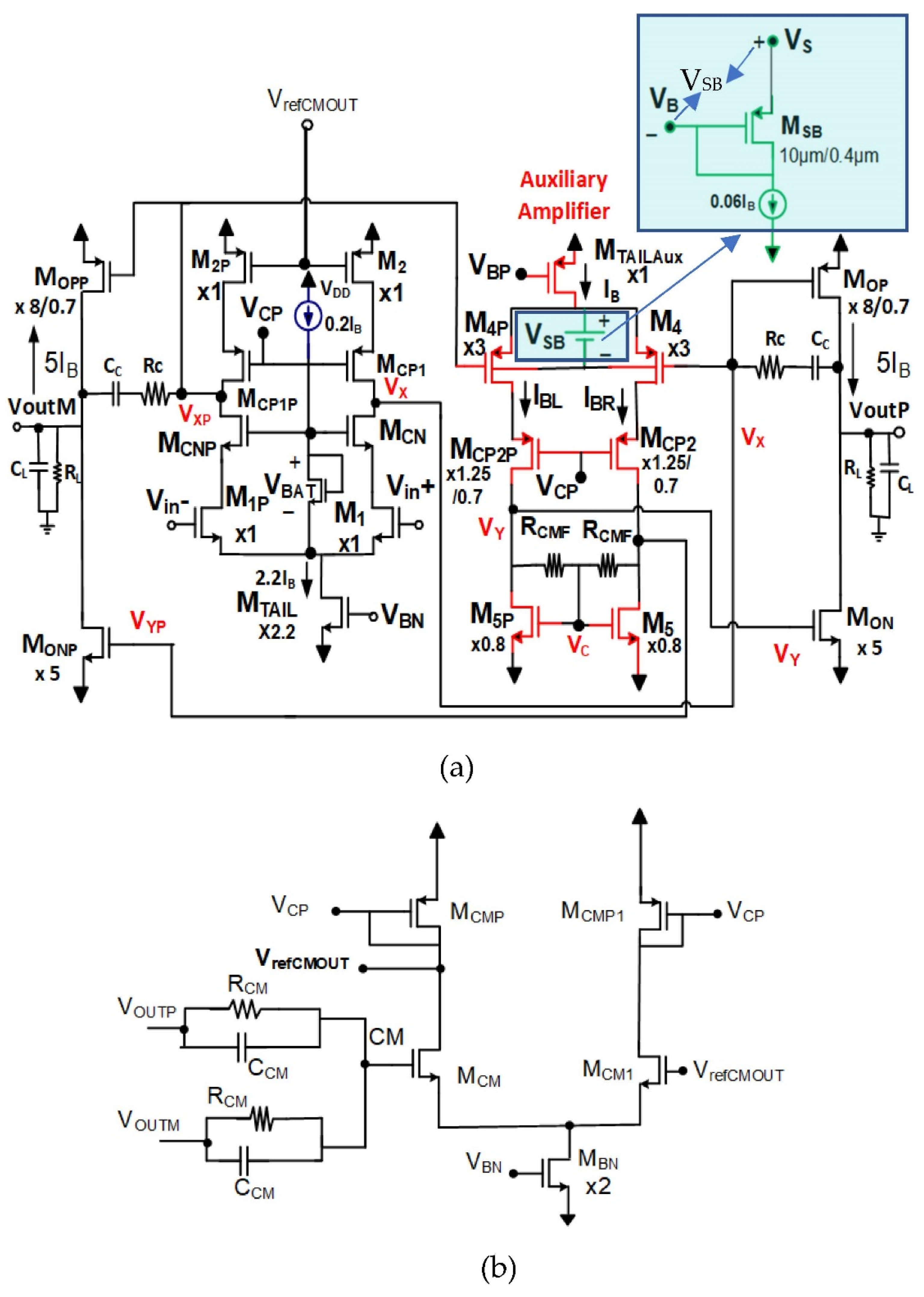
The proposed class-AB op-amp shown in Figure 1 is a fully differential operational amplifier that can drive a wide range of resistive and capacitive loads. The op-amp uses a high gain telescopic input stage to keep a high DC open-loop gain even for low-valued resistive loads (high resistive loading conditions) that degrade the gain of the output stage and push-pull class AB output stages. Conventional Miller compensation is used to achieve stability over a wide range of loading conditions. The main contribution of this paper is the utilization of a compact, fully differential auxiliary amplifier (AuxAmp) that is used to achieve power-efficient class AB operation and improved unity gain frequency fu in the proposed op-amp. As discussed in detail below, this approach offers several advantages with respect to conventional class AB schemes: it generates signal voltages VY and VYP that are amplified versions and in phase with VX and VXP. In order to have enough headroom for the auxiliary amplifier’s input differential pair (M4, M4P), a floating battery VSB is used to reduce the threshold voltage of M4, M4P. This floating battery is implemented using a diode-connected PMOS transistor with a minimal quiescent current, just like VBAT in the input stage is used. In addition, M4 and M4P are scaled up by a factor of three. This is to reduce their drain-source saturation voltage VDSsat. A resistive local common-mode feedback (RLCMFB) network is used as a load in order to obtain moderate gain AAux from the AuxAmp. The non-inverting gain of the auxiliary amplifier is given approximately by . The AuxAmp increases the overall open-loop gain, the unity-gain frequency, and significantly the peak negative output currents and slew-rate of the op-amp. This AuxAmp also assists the proposed op-amp in maintaining an accurate output quiescent current IOutQ minimizing the effect of temperature, supply voltage variations, and technology parameter variations on IOutQ. The quiescent gate voltages VY, VYP of transistors MON,ONP control the quiescent output current IoutQ. Under quiescent conditions, no current flows in resistors RCMF, and the gate-source voltage of MON,ONP is VY = VYP = VGS5P,5Q, independent of the value of RCMF that sets the gain AAux. The AuxAmp consumes only 6% of the total op-amp quiescent current, which helps to keep the op-amp’s current efficiency high.

Figure 1.
(a) Proposed fully differential op-amp. (b) Common-mode feedback network.
2.1. Operation
In the presence of positive input differential signals, the voltage at node VX decreases and at VXP increases, while the voltages at node VY decrease and at node VYP increase by a factor AAux. As a result, MOP will provide a large output positive current and MONP a large negative output current. The drain currents of MON, MOPP will decrease and eventually reach zero. Similarly, MON can provide large negative output currents for negative input signals, and MOPP can provide large positive output currents as the voltage at VXP decreases. In the conventional floating battery scheme where variations VX, VXP are transferred directly to VY, VYP, the maximum negative output current is limited by the relatively small positive excursion of VX, VXP transferred to VY, VYP. In the proposed scheme, the gain AAux increases significantly the excursion of VY, VYP and the peak negative output current. AAux also increases the open-loop gain, common-mode rejection ratio (CMRR), power supply rejection ratio (PSRR), and unity gain frequency of the op-amp.
2.2. Frequency Response
The gain of the telescopic input stage AI is given by (1).
For simplicity, it is assumed that gm and ro are the transconductance gain and output resistance of all unit size NMOS and PMOS transistors, and RX is resistance at nodes VX, VXP.
The single-ended gain of the auxiliary amplifier is given by . RY,YP is the resistance at nodes VY and VYP: where . The value of the RCMF is selected in such a way so that . As a result, RY can be approximated as RY ≈ RCMF. Thus, gain of the auxiliary amplifier can be expressed approximately by (2).
The gain of the output stage is given by (3).
where Rout is . gmOP and gmON are transconductance gains of output transistors MOP and MON.
Thus, the open-loop DC gain AOLDC of the proposed op-amp is expressed by (4).
where .
The dominant pole is at node VX, XP, and is given by (5).
Here, CX is given by .
The gain-bandwidth product (GBW) of the proposed op-amp is given by the expression (6).
Aout is strongly dependent on RL. For very low RL values, it can even take values |Aout| < 1. Besides the dominant pole, the proposed op-amp has two pairs of high-frequency poles: one at VY (VYP) and another at VoutP (VoutM). The output high-frequency pole fPout is given in (7).
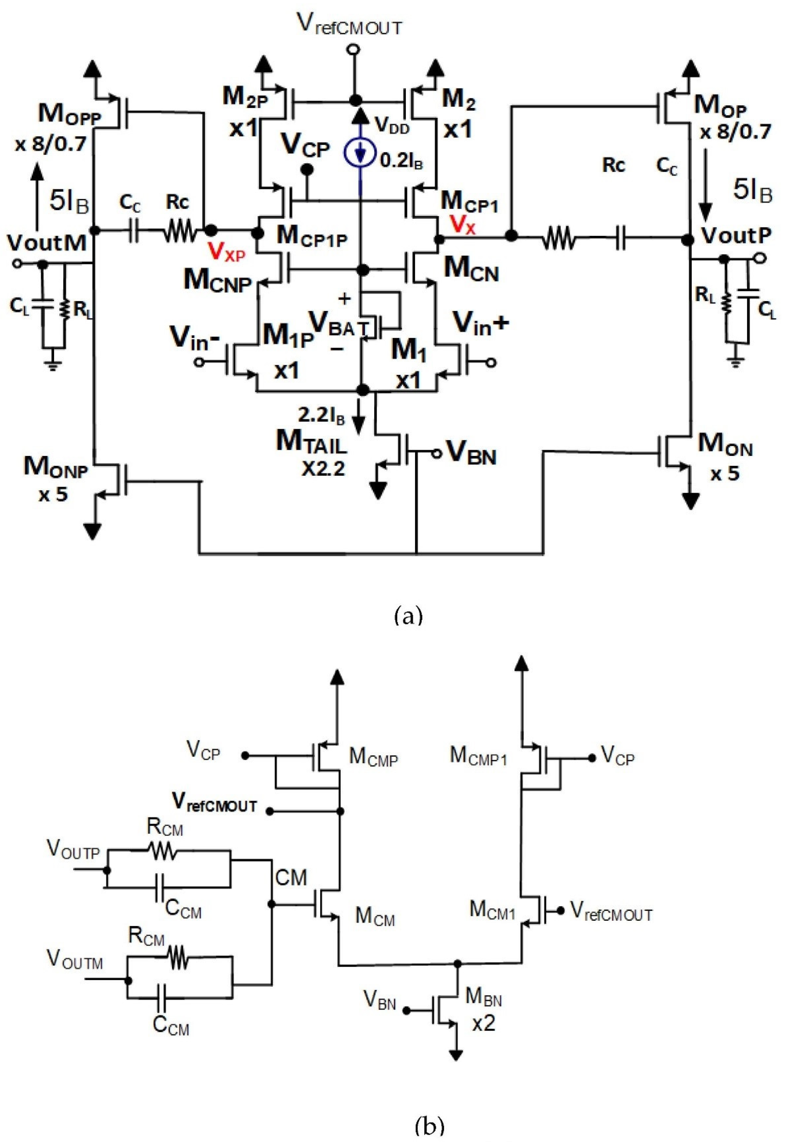
In the proposed op-amp, the auxiliary amplifier causes fPout to be higher than output pole frequency fPout_conv of the conventional op-amp shown in Figure 2. The high-frequency output pole of the conventional op-amp of Figure 2 is given in (8).
where gmOP_conv is the transconductance gain of the output PMOS transistor of the conventional op-amp. The value of fPout of the proposed op-amp for CL = 300 pF and RL = 1 MΩ is 6 MHz, whereas the output pole frequency for the conventional-A op-amp fPout_conv is only 687 kHZ for a similar loading condition.
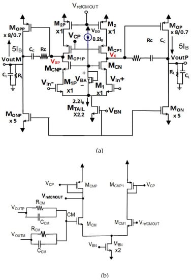
Figure 2.
(a) Conventional Class-A amplifier. (b) Common-mode feedback network.
It can be seen that the auxiliary amplifier in the proposed op-amp shifts the output pole to a higher frequency. Consequently, a higher unity gain frequency can be obtained in the proposed op-amp.
The pole at nodes VY, VYP is expressed by (9).
Here, CY is given by .
From (9), it can be said that the location of the poles (fPY) at node VY,YP depends on the value of RCMF. The high-frequency pole fPY is inversely proportional to the value of RCMF, i.e., . Again from (2), it can be seen that the gain of the auxiliary amplifier depends on the value of RCMF, i.e., . Thus, the selection of RCMF plays an essential role in determining the stability, overall open-loop gain, and slew-rate improvement of the proposed op-amp as the gain of the auxiliary control of the dynamic current of MON,ONP. In the proposed circuit, the value of the RCMF is 60 kΩ. This selection of RCMF helps to place fPY at a higher frequency than the unity gain frequency of the op-amp. The higher value of fpY helps achieve approximately constant gain from the auxiliary amplifier until the proposed op-amp’s unity gain frequency. The value of the fPY in the proposed op-amp is 29 MHz, which is twice larger than the unity gain frequency of the proposed op-amp.
The zero is given by (10).
3. Results
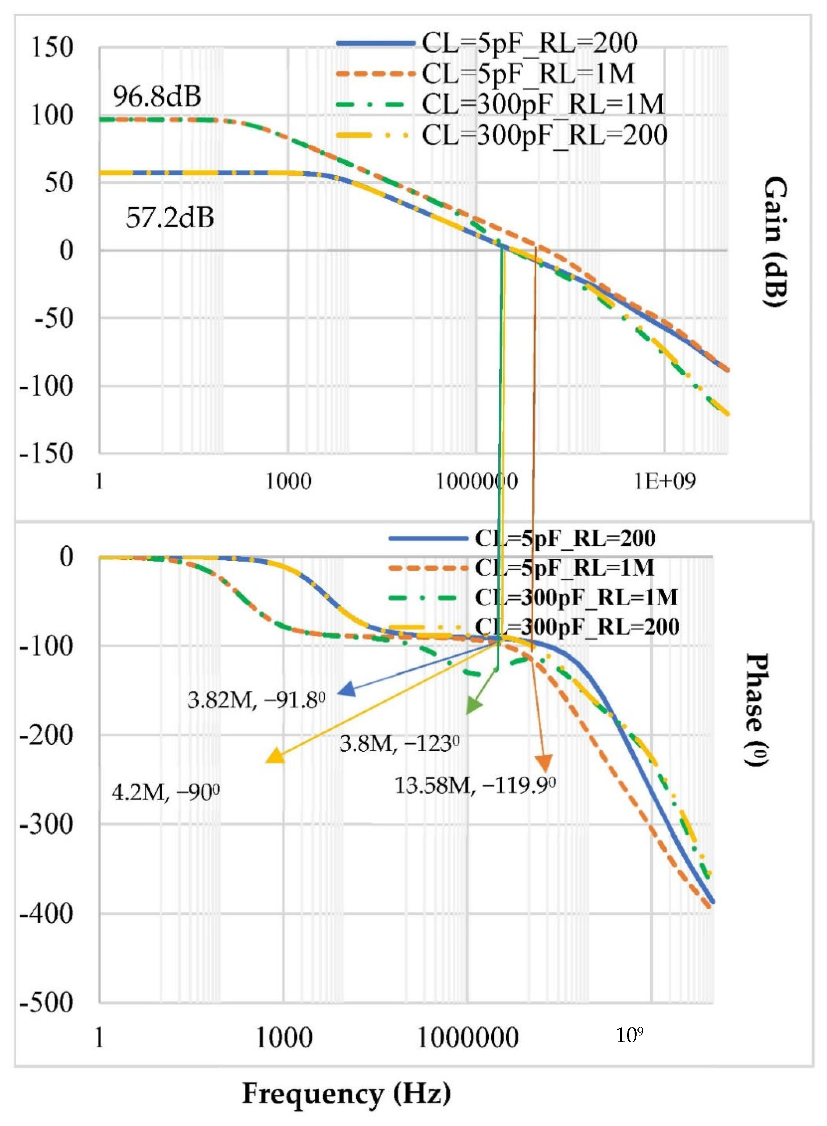
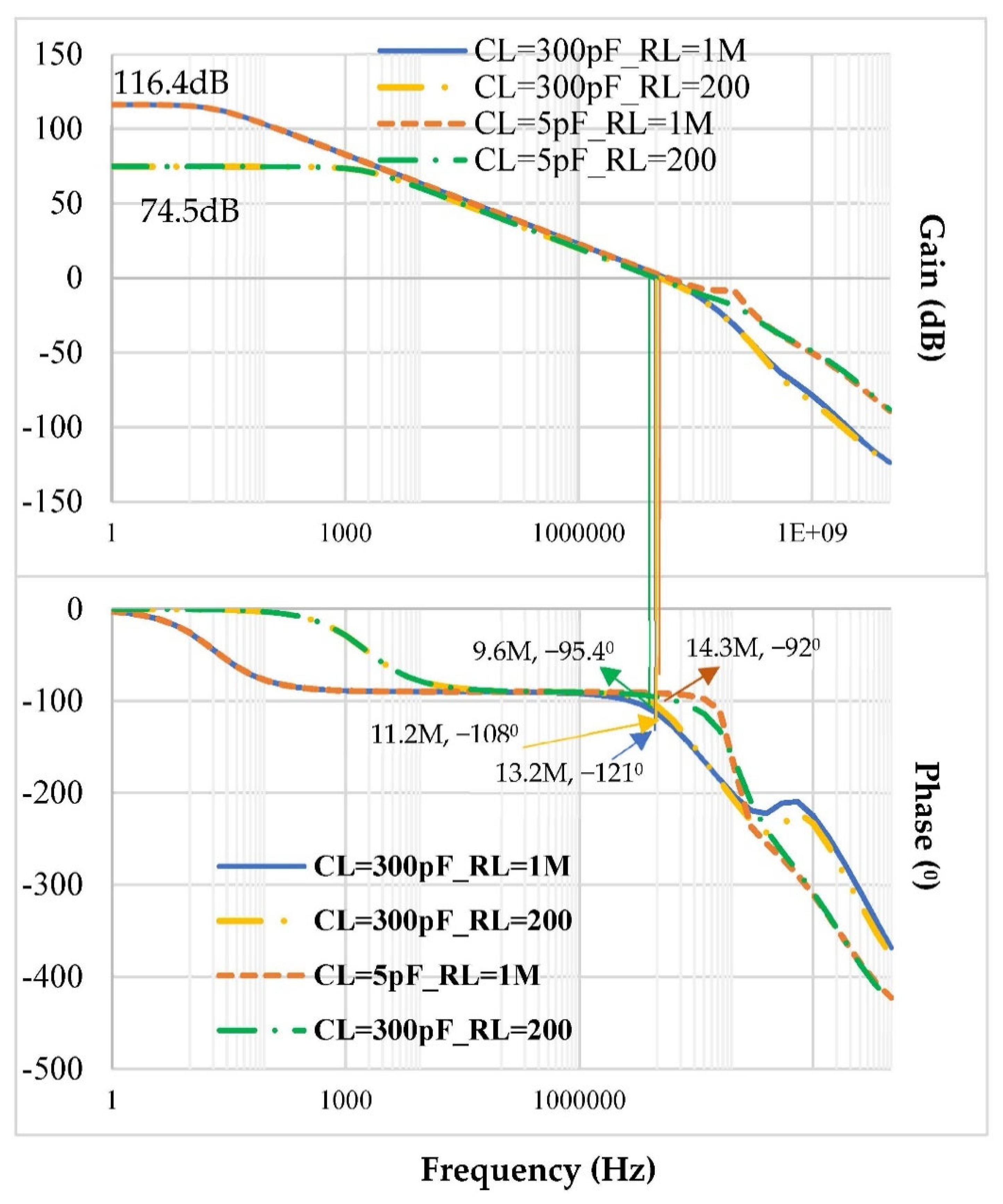
The proposed and conventional class-A (Conv-A) op-amps are simulated with Cadence using TSMC 180 nm CMOS technology parameters. For a fair comparison, equal unit size pMOS and nMOS transistors with W/L = 10 µm/0.4 µm are used in both op-amps. The output nMOS and pMOS transistors are scaled up by the factors 5/1 and 8/0.7 with respect to unit size transistors. The value of the compensation capacitor is 3 pF for both op-amps. The only difference between the proposed and Conv-A op-amp is that the Conv-A op-amp does not have the auxiliary amplifier, which only increases power dissipation by 6%. The schematic diagram of the Conv-A amplifier is given in Figure 2. The value of the RCMF used in the auxiliary amplifier of the proposed op-amp is 60 kΩ. The values of RC in the proposed op-amp are 200 Ω and 6 kΩ for the capacitive loads CL = 5 pF and 300 pF, respectively. For the fixed CL, the selected compensation network can drive RL values from 1 MΩ to 200 Ω, whereas in the conventional op-amp for a similar capacitive load CL = 300 pF and 5 pF, the values of RC are 18 kΩ and 500 Ω. A bias current IB = 17 µA, dual supply voltages VDD = 900 mV, VSS = −900 mV, and a reference common-mode output voltage VrefCM = 0 V are used for the simulations of both op-amps. Figure 3 and Figure 4 show open-loop frequency responses of the Conv-A and the proposed op-amps. It can be seen from the responses that both op-amps are stable for the wide range of capacitive (5 pF–300 pF) and resistive load (200 Ω–1 MΩ). However, the proposed op-amp’s gain is higher and varies from 116.4 dB to 74.5 dB for RL, changing from 1 MΩ to 200 Ω. For similar loading conditions, the Conv-A op-amp has the gain that varies from 96.8 dB to 57.2 dB. The proposed op-amp achieves a higher gain because of the auxiliary amplifier.
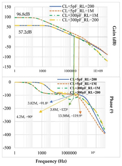
Figure 3.
Frequency response of Conv-A op-amp.
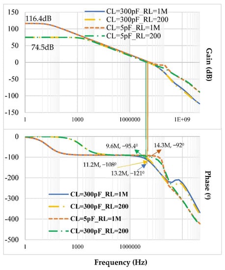
Figure 4.
Frequency response of proposed op-amp.
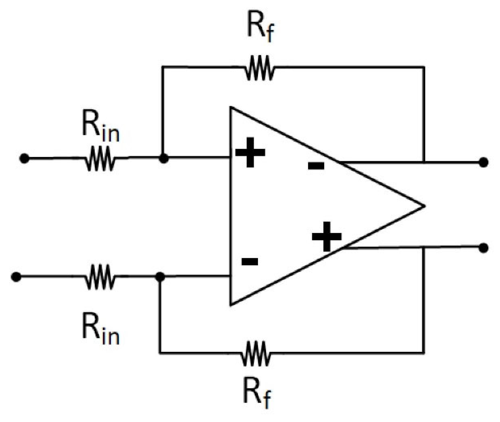
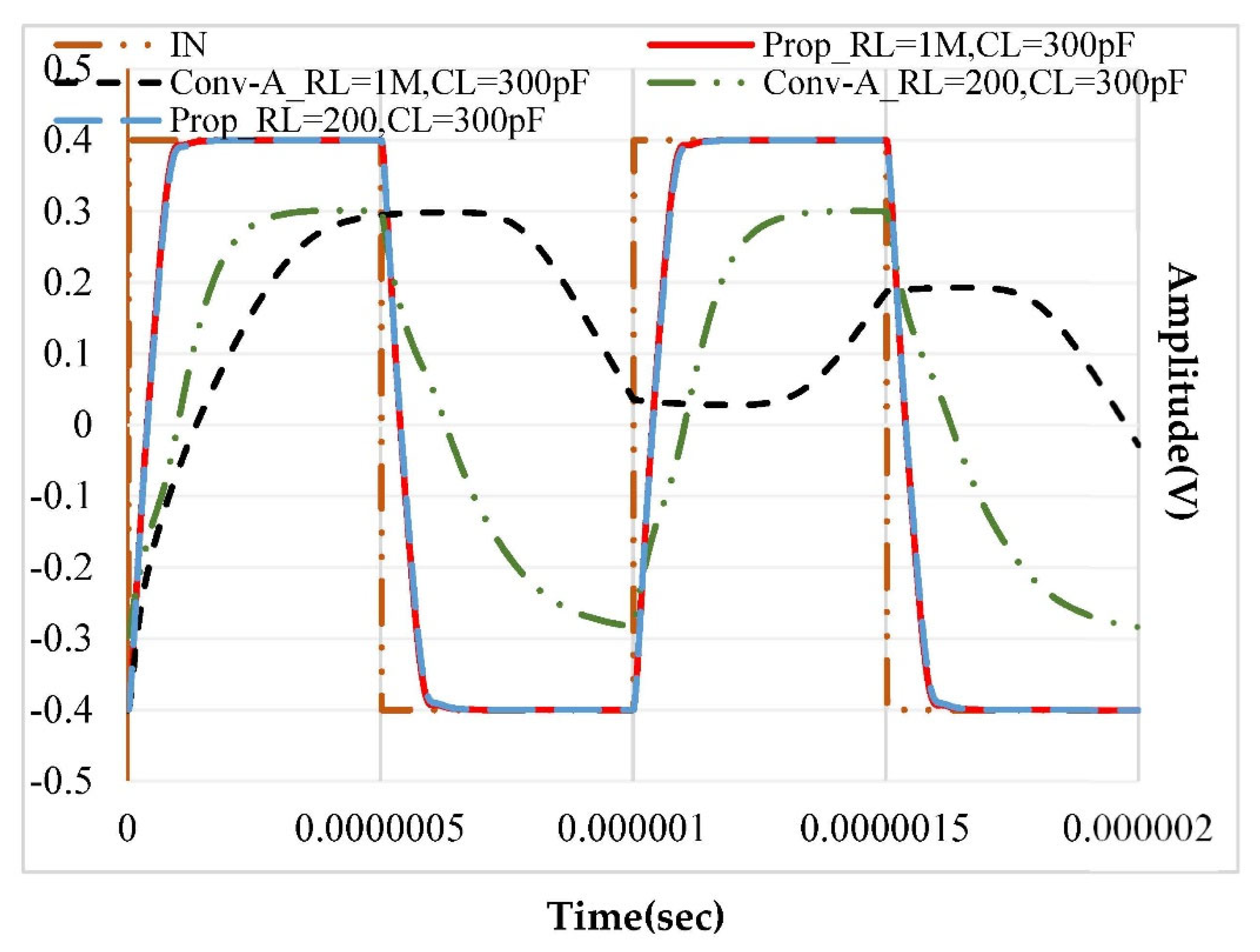
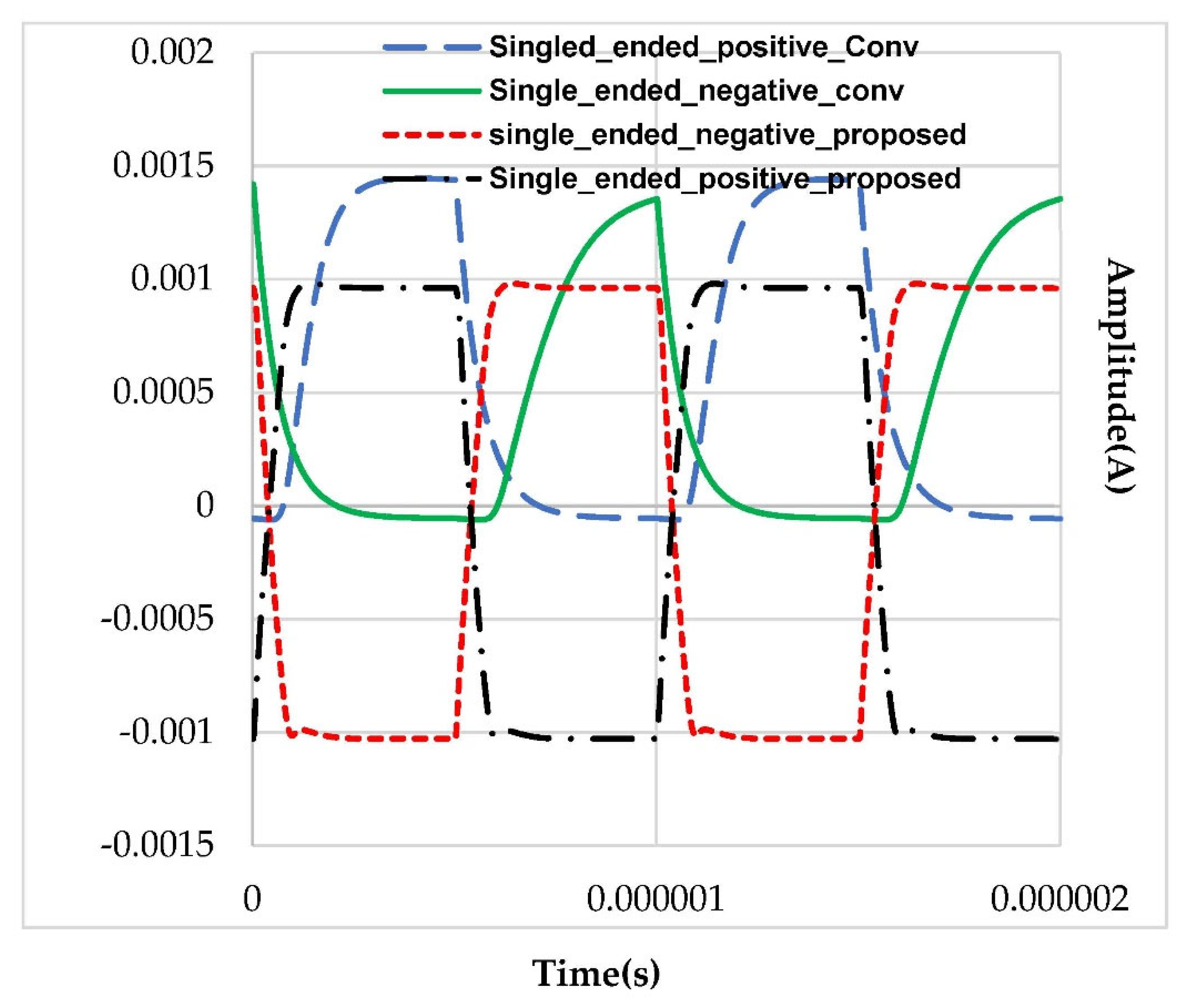
The transient response of the proposed op-amp was simulated using the unity gain closed loop inverting amplifier configuration, shown in Figure 5. Equal Rin and Rf values of 100 kΩ were used in the simulation. Figure 6 shows the transient response of the proposed and Conv-A op-amps in unity gain inverting configuration for a 1 MHz, ±400 mVpp pulse input, with CL = 300 pF and two resistive load values RL = 200 Ω and 1 MΩ. From the pulse response, it can be seen that the Conv-A op-amp cannot follow the input pulse, whereas the proposed op-amp can follow the input for all the considered loading conditions. The proposed op-amp has a slew rate of 13 V/µs, whereas the Conv-A op-amp has a much lower slew rate of 0.9 V/µs. The proposed op-amp can provide ±4.36 mA peak currents to a 300 pF capacitor. On the contrary, the Conv-A op-amp can provide only 58 µA peak negative output currents, which corresponds to the class-A op-amp’s output quiescent current (IoutQ). Figure 7 shows the single-ended output currents of both op-amps in the 200 Ω resistive load for ±400 mV pulse input. It can be seen that due to the substantial limitation of the negative current in the Conv-A op-amp, the outputs cannot follow the negative excursion of the input pulse. As a result, the op-amp cannot provide differential complementary output signals. It can be seen that the peak negative current is –58 μA. On the other hand, the proposed op-amp can provide complementary output signals with equal positive and negative output currents of ±1 mA in the 200 Ω resistive loads for the ±200 mV pulse input.
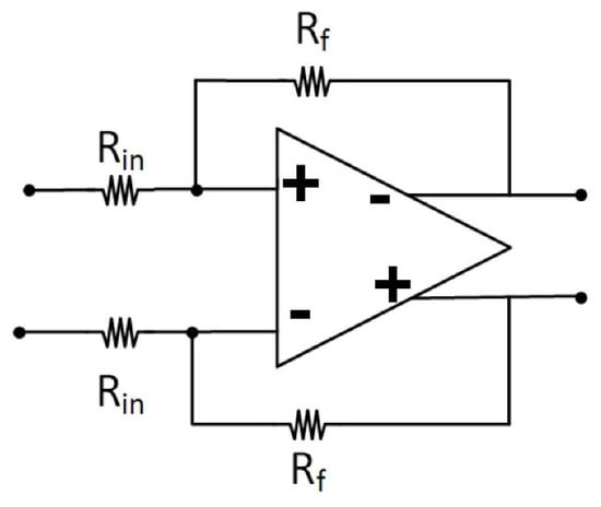
Figure 5.
Unity gain inverting fully differential amplifier.
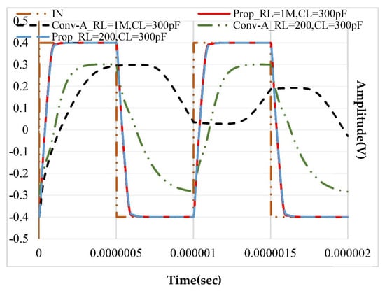
Figure 6.
Pulse response of the proposed and conventional op-amp, CL = 300 pF and RL = 1 MΩ and 200 Ω.
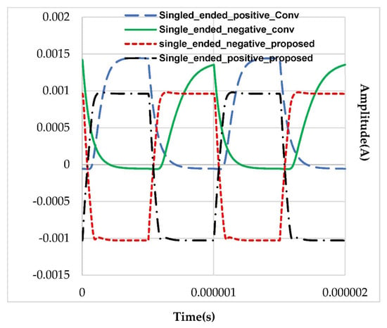
Figure 7.
Single-ended transient current in RL = 200 Ω of the proposed and Conv-A op-amp for ±400 mV pulse input.
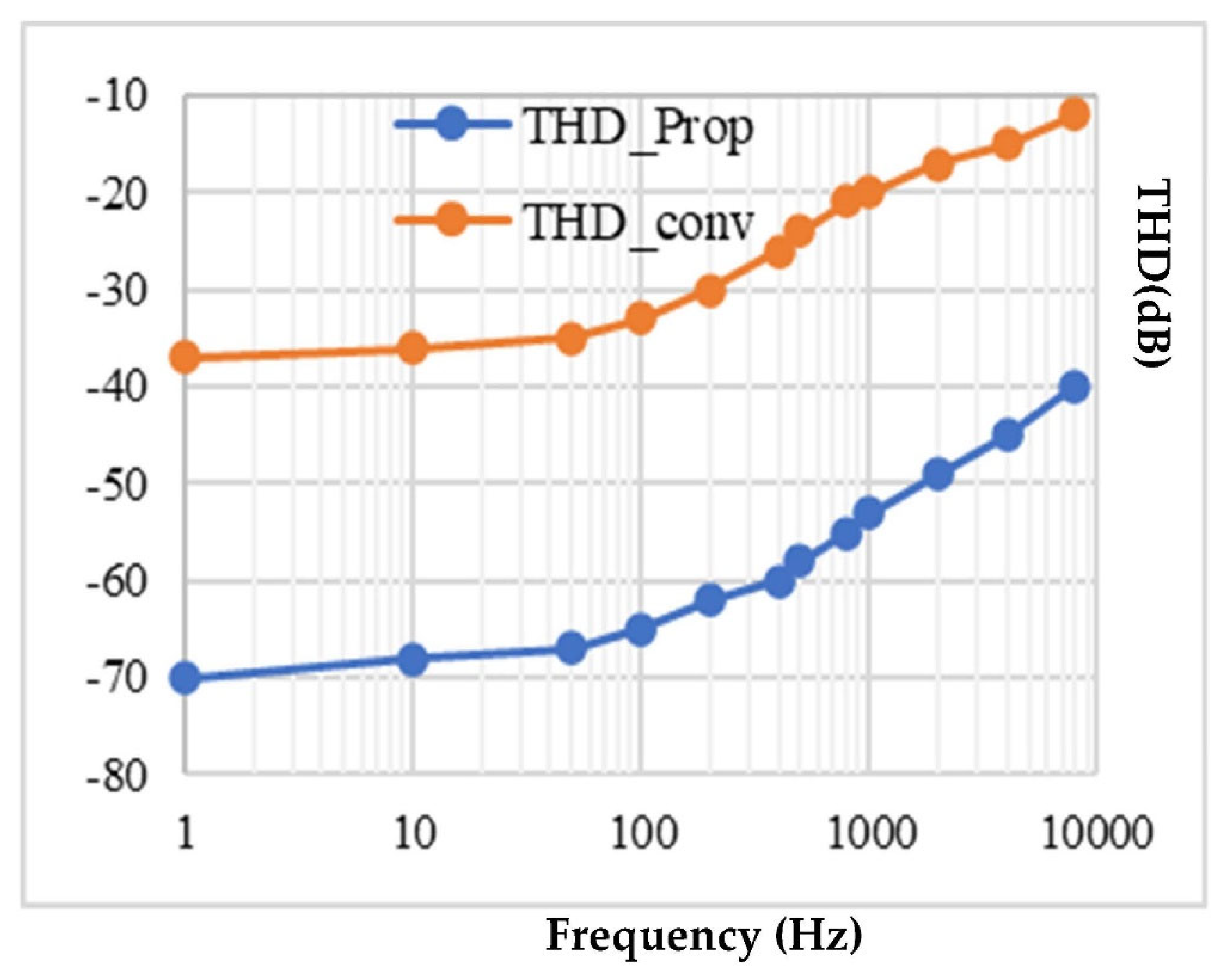
Figure 8 shows the output current of the proposed and Conv-A op-amp for CL = 300 pF, 5 pF, and RL = 1 MΩ for the ±400 mVpp 1 MHz pulse input. The proposed op-amp can provide ±4.36 mA peak currents to 300 pF load capacitors. On the contrary, the Conv-A op-amp can provide only 58 µA negative output, which corresponds to the class-A op-amp’s output quiescent current (IoutQ). Figure 9 shows the total harmonic distortion of the proposed and Conv-A op-amp for a 400 mV amplitude sinusoidal signal whose frequency is varied from 1 kHz to 8 MHz. It can be seen that the proposed op-amp has much lower (35 dB) harmonic distortion than the Conv-A op-amp.
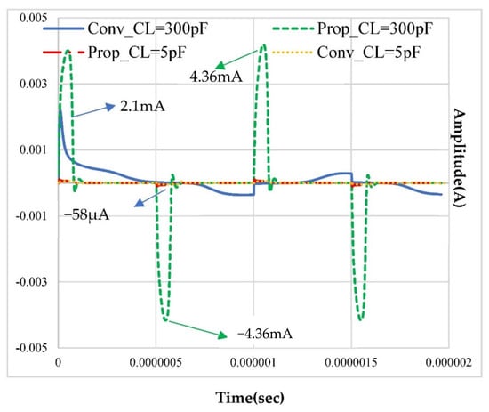
Figure 8.
Output current of the proposed and conventional op-amp for CL = 300 pF, 5 pF and RL = 1 MΩ for the ±400 mVpp, 1 MHz pulse input.
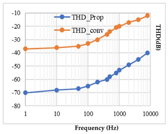
Figure 9.
THD of the proposed op-amp at different frequencies for 400 mV amplitude sinusoidal signal and RL = 200 Ω, CL = 300 pF.
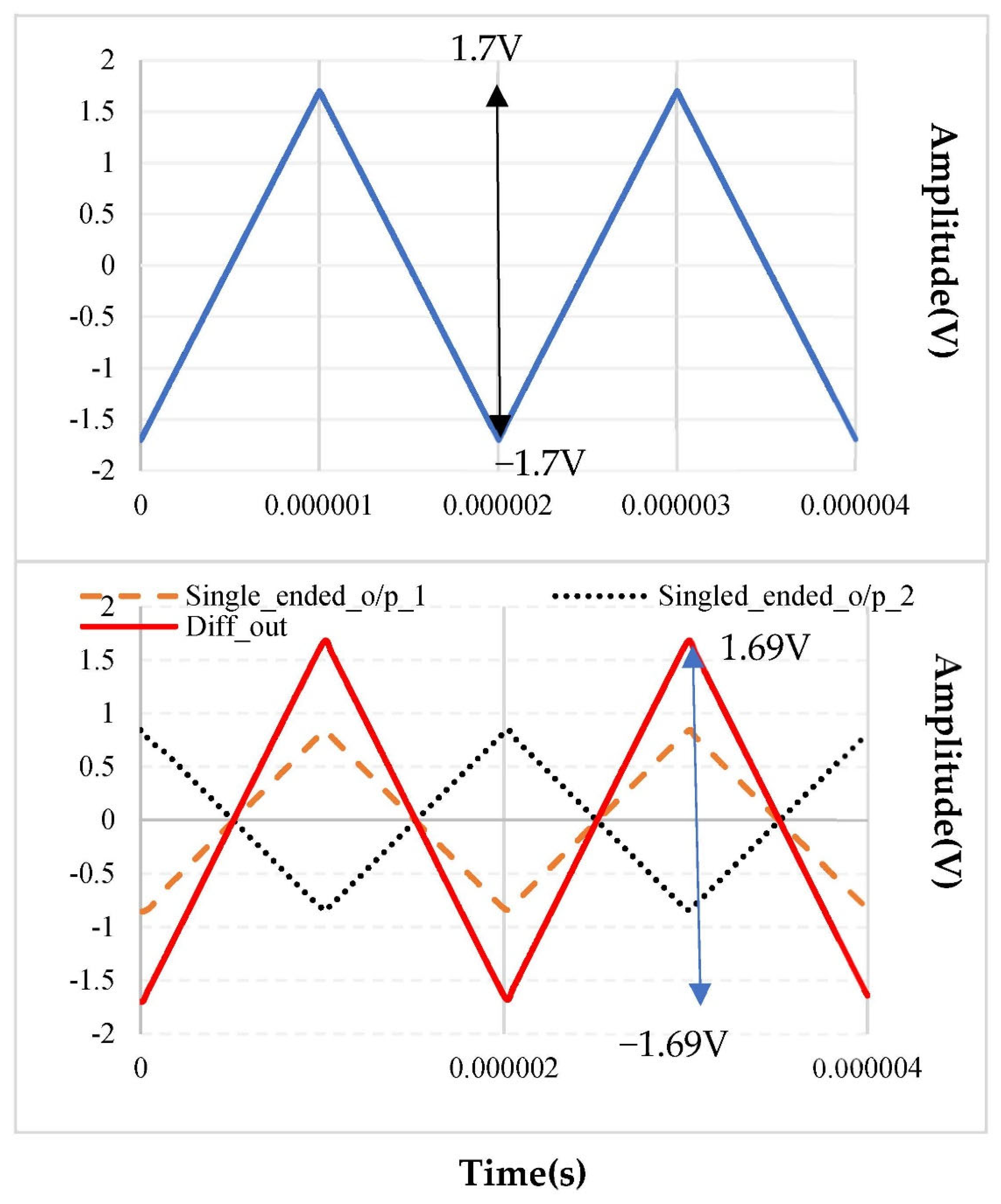
The proposed op-amp has close to rail-to-rail output swing from −1.69 V to 1.69 V for a ±1.7 V, 0.5 MHz triangular input signal. It can be seen in Figure 10. Table 1, Table 2 and Table 3 show the corner analysis of the proposed op-amp at different temperatures. It can be asserted that the proposed op-amp is robust against the variation of process technology and temperature. The standard deviation (Std.) for each parameter at different corners is calculated for each considered temperature and given in the table. The common-mode rejection ratios (CMRRs) and power supply rejection ratios (PSRRs) are measured, including 2% typical mismatches between the differential pair transistors in both op-amps. The positive and negative PSRRs are 95 dB and 92 dB. The CMRR of the proposed op-amp is 96 dB. Table 4 shows comprehensive simulation results of the proposed op-amp and comparisons of the performance with state-of-the-art works. The proposed op-amp has the highest static and dynamic current efficiency figures of merit.
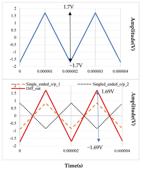
Figure 10.
Determination of close to rail-to rail output swing using a ±1.7 V, 0.5 MHz, triangular input signal.

Table 1.
Corner analysis of op-amp at T = −20 °C.

Table 2.
Corner analysis of op-amp at T = 27 °C.

Table 3.
Corner analysis of op-amp at T = 120 °C.

Table 4.
Summary of the simulated results and performance comparison.
4. Conclusions
The proposed fully differential op-amp can drive a wide range of resistive (200 Ω–1 MΩ) and capacitive (5–300 pF) loads. A compact auxiliary amplifier is used in the op-amp. This sets a well-controlled output quiescent current and increases the op-amp’s unity gain frequency, significantly the peak negative output current. The proposed op-amp has high dynamic and static current efficiencies as well as a large and small-signal figure of merit. The auxiliary amplifier consumes only 6% of the total op-amp current, making the proposed op-amp highly power-efficient.
Author Contributions
Investigation, writing, review, and editing were completed by A.P., J.R.-A., H.V.-L., J.H.-C. and A.D.-S. All authors have read and agreed to the published version of the manuscript.
Funding
This research received no external funding.
Institutional Review Board Statement
Not applicable.
Informed Consent Statement
Not Applicable.
Data Availability Statement
Data is contained within the article.
Conflicts of Interest
There is no conflict of interest.
References
- Walden, R.H. Analog-to-digital converter survey and analysis. IEEE J. Sel. Areas Commun. 1999, 17, 539–550. [Google Scholar] [CrossRef] [Green Version]
- Karki, J. Fully differential amplifier design in high-speed data acquisition systems. Analog Des. J. 2002. Available online: https://www.ti.com.cn/cn/lit/an/slyt034/slyt034.pdf#page=35 (accessed on 26 December 2021).
- Kobayashi, H.; Kushita, N.; Tran, M.T.; Asami, K.; San, H.; Kuwana, A.; Hatta, A. Analog/Mixed-Signal/RF Circuits for Complex Signal Processing. In Proceedings of the 2019 IEEE 13th International Conference on ASIC (ASICON), Chongqing, China, 29 October–1 November 2019; pp. 1–4. [Google Scholar]
- Gray, P.R.; Hurst, P.J.; Lewis, S.H.; Meyer, R.G. Analysis and Design of Analog Integrated Circuits, 5th ed.; Wiley: Hoboken, NJ, USA, 2001. [Google Scholar]
- Spinelli, E.M.; Haberman, M.A.; Guerrero, F.N.; García, P.A. A High Input Impedance Single-Ended Input to Balanced Differential Output Amplifier. IEEE Trans. Instrum. Meas. 2020, 69, 1682–1689. [Google Scholar] [CrossRef]
- Banu, M.; Khoury, J.M.; Tsividis, Y. Fully differential operational amplifiers with accurate output balancing. IEEE J. Solid-State Circuits 1988, 23, 1410–1414. [Google Scholar] [CrossRef]
- Hassan, A.H.; Mostafa, H.; Salama, K.N.; Soliman, A.M. A Low-Power Time-Domain Comparator for IoT Applications. In Proceedings of the 2018 IEEE 61st International Midwest Symposium on Circuits and Systems (MWSCAS), Windsor, ON, Canada, 5–8 August 2018; pp. 1142–1145. [Google Scholar]
- Razavi, B. Design of Analog CMOS Integrated Circuits, 1st ed.; McGraw-Hill: New York, NY, USA, 2001. [Google Scholar]
- Monticelli, D.M. A quad CMOS single-supply op amp with rail-to-rail output swing. IEEE J. Solid-State Circuits 1986, 21, 1026–1034. [Google Scholar] [CrossRef] [Green Version]
- Langen, K.D.; Huijsing, J.H. Compact low-voltage power-efficient operational amplifier cells for VLSI. IEEE J. Solid-State Circuits 1998, 33, 1482–1496. [Google Scholar] [CrossRef] [Green Version]
- Pang-Cheng, Y.; Jiin-Chuan, W. A class-B output buffer for flat-panel-display column driver. IEEE J. Solid-State Circuits 1999, 34, 116–119. [Google Scholar] [CrossRef]
- Gregorian, R.; Temes, G.C. Analog MOS Integrated Circuits for Signal Processing, 1st ed.; Wiley Series on Filters: Design Manufacturing and Applications; Wiley: Hoboken, NJ, USA, 1986. [Google Scholar]
- Aloisi, W.; Giustolisi, G.; Palumbo, G. A 1-V CMOS output stage with high linearity. In Proceedings of the 2003 International Symposium on Circuits and Systems, 2003. ISCAS’ 03., Bangkok, Thailand, 25–28 May 2003; p. I. [Google Scholar]
- Grasso, A.D.; Palumbo, G.; Pennisi, S. Advances in Reversed Nested Miller Compensation. IEEE Trans. Circuits Syst. I Regul. Pap. 2007, 54, 1459–1470. [Google Scholar] [CrossRef]
- Sutula, S.; Dei, M.; Terés, L.; Serra-Graells, F. Variable-Mirror Amplifier: A New Family of Process-Independent Class-AB Single-Stage OTAs for Low-Power SC Circuits. IEEE Trans. Circuits Syst. I Regul. Pap. 2016, 63, 1101–1110. [Google Scholar] [CrossRef] [Green Version]
- Kuo, P.Y.; Tsai, S.D. An Enhanced Scheme of Multi-Stage Amplifier With High-Speed High-Gain Blocks and Recycling Frequency Cascode Circuitry to Improve Gain-Bandwidth and Slew Rate. IEEE Access 2019, 7, 130820–130829. [Google Scholar] [CrossRef]
- Basumata, U.; Mondal, A.; Das, S.; Rahaman, H. Design of Two-Stage Fully-Differential Driver in SAR ADC with Indirect Feedback Compensation Technique. In Proceedings of the 2021 International Symposium on Devices, Circuits and Systems (ISDCS), Vellore, India, 3–5 March 2021; pp. 1–5. [Google Scholar]
- Ahmed, M.; Shah, I.; Tang, F.; Bermak, A. An improved recycling folded cascode amplifier with gain boosting and phase margin enhancement. In Proceedings of the 2015 IEEE International Symposium on Circuits and Systems (ISCAS), Lisbon, Portugal, 24–27 May 2015; pp. 2473–2476. [Google Scholar]
- Shamsi, H.; Anisheh, S.; Abbasizadeh, H.; Dadkhah, C.; Lee, K.-Y. A 84 dB DC-Gain Two-Stage Class-AB OTA. IET Circuits Devices Syst. 2019, 13, 614–621. [Google Scholar] [CrossRef]
- Neag, M.; Kovács, I.; Oneț, R.; Câmpanu, I. Design options for high-speed OA-based fully differential buffers able to drive large loads. Microelectron. J. 2021, 114, 105115. [Google Scholar] [CrossRef]
- Renteria-Pinon, M.; Ramirez-Angulo, J.; Diaz-Sanchez, A. Simple Scheme for the Implementation of Low Voltage Fully Differential Amplifiers without Output Common-Mode Feedback Network. J. Low Power Electron. Appl. 2020, 10, 34. [Google Scholar] [CrossRef]
Publisher’s Note: MDPI stays neutral with regard to jurisdictional claims in published maps and institutional affiliations. |
© 2022 by the authors. Licensee MDPI, Basel, Switzerland. This article is an open access article distributed under the terms and conditions of the Creative Commons Attribution (CC BY) license (https://creativecommons.org/licenses/by/4.0/).

