Abstract
The energy of real-time systems for embedded usage needs to be efficient without affecting the system’s ability to meet task deadlines. Dynamic body bias (BB) scaling is a promising approach to managing leakage energy and operational speed, especially for system-on-insulator devices. However, traditional energy models cannot deal with the overhead of adjusting the BB voltage; thus, the models are not accurate. This paper presents a more accurate model for calculating energy overhead using an analytical double exponential expression for dynamic BB scaling and an optimization method based on nonlinear programming with consideration of the real-chip parameter constraints. The use of the proposed model resulted in an energy reduction of about 32% at lower frequencies in comparison with the conventional model. Moreover, the energy overhead was reduced to approximately 14% of the total energy consumption. This methodology provides a framework and design guidelines for real-time systems and computer-aided design.
1. Introduction
Power consumption has become an important factor, especially for real-time systems (RTSs) for embedded usage that must meet task deadlines. The computational node in such systems often works intermittently with a certain interval. Reducing leakage power consumption in sleep mode has become a major concern as technology feature size continues to scale.
RTS energy efficiency has been extensively studied, and several techniques have been developed for saving energy, including dynamic power management (DPM) [1] such as power gating (PG) [2] and dynamic voltage scaling (DVS) [3]. Although these techniques improve energy efficiency, they often require a significant amount of power, since they must directly control the system supply voltage. When the supply voltage is in the near-threshold region, the range of power-supply scaling is restricted [4]. Moreover, the application of PG results in the loss of th e data in the memory element. Thus, PG often introduces serious problems in embedded systems.
Body bias (BB) control is attracting the attention of designers as a means of controlling the tradeoff between leakage power and performance without affecting power supply [5,6]. It is especially efficient in fully depleted silicon-on-insulator (FD-SOI) technology [7,8,9], which is commonly used for low-power systems.
Previous studies on dynamic BB control [5,10,11] have two limitations. First, they were not based on a model of BB switching-voltage overhead. Most of them ignored it or included the energy consumption in the active state. Second, a method has not been proposed for finding the optimal BB voltage and the optimal supply voltage for meeting task deadlines.
Some Internet of Things (IoT) devices work with a long interval and thus have a task deadline of more than a few seconds. The overhead of switching the body bias (BB) voltage is hence trivial. On the other hand, since the GPS time period is millisecond-order, the deadline for locating mobile devices is often millisecond-order. Some factory automation tasks also require a millisecond-order deadline. Precise power optimization techniques are thus required to cope with such newly developed applications. We have devised a standard full switching impulse voltage (double exponential) expression [12,13,14], and a mathematical expression of the transient for estimating the switching energy. We also devised an interior point method (IPM) based on this power model that can be used to obtain optimality in nonlinear programming (NLP). The main contributions of this study can be summarized as follows:
- A mathematical model for calculating energy overhead based on the double exponential equation,
- increasing the accuracy of the energy overhead calculation model, and
- a method for optimizing energy consumption by optimizing the BB voltage and supply voltage by applying NLP.
This methodology provides a framework and design guidelines for RTSs and computer-aided design (CAD).
This paper is organized as follows. Section 2 describes BB, FD-SOI technology, and related work on energy reduction. Section 3 explains the mathematical power model and introduces the concept of the double exponential waveform. In addition, it introduces the term for increasing the accuracy of the energy overhead. The energy consumption optimization method is described in Section 4. The experimental results are presented, analyzed, and discussed in Section 5 along with the method for increasing the accuracy of the energy overhead calculation model. Finally, Section 6 concludes the paper and mentions future work.
2. Background
2.1. BB for Silicon on Thin Box
Our target technology is silicon-on-thin-box (SOTB) technology, a novel FD-SOI technology [7]. It features latch-up immunity, high temperature tolerance, high performance, radiation hardness, and high BB sensitivity due to its insulating buried oxide layer, which is widely used in SOI devices [8,9]. These body-driven characteristics enable high-level energy reduction using BB. Unlike conventional FD-SOI devices, an SOTB device is formed on an ultra-thin box layer (about 10 nm thick), as shown in Figure 1, enabling a wide range of BB control. Consequently, SOTB technology ensures more efficient reduction in leakage current using BB control than conventional metal-oxide semiconductor field-effect transistors (MOSFETs).
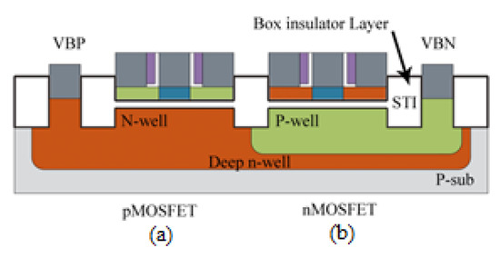
Figure 1.
Cross-sectional view of silicon-on-thin-box (SOTB) metal-oxide semiconductor field-effect transistors (MOSFETs): (a) pMOS and (b) nMOS.
The SOTB states are classified in accordance with the nMOS BB voltage , the pMOS BB voltage , and the supply voltage . As with other FD-SOI technologies, the default state of a given MOSFET ( and ) in SOTB technology is called zero body bias (ZBB). If a lower voltage is applied to the nMOS body (VBN<0) and a higher voltage is applied to the pMOS body (VBP>VDD), the depletion width increases; thus, the threshold voltage increases. This condition is known as reverse body bias (RBB). With RBB, since the threshold voltage is higher, the leakage current is lower at the expense of an increase in the delay time, so performance is degraded.
In contrast, if a higher voltage is applied to the nMOS body (VBN>0) and a lower voltage is applied to the pMOS body (VBP<VDD), the depletion width decreases; therefore, the threshold voltage decreases. This condition is known as forward body bias (FBB). With FBB, since the threshold voltage is lower, the delay is reduced at the expense of an increase in the leakage current. We use balanced BB such that , which normally results in the best performance per energy [11]. Thus, BB is represented simply as hereafter.
2.2. Related Work
Since energy efficiency is essential in embedded RTSs, several techniques have been developed for saving energy, and much research has been carried out on saving energy by controlling the power supply and clock frequency. The DPM technique reduces the energy dissipation of RTSs with low-power idle states [1]. However, when the power supply is cut off during the idle state, volatile data are lost. Hence, when data need to be preserved, a certain level of voltage must be supplied as a power supply, which restricts the leakage power reduction. The DVS technique can drastically reduce the dynamic power due to the quadratic power supply dependency [3]. However, the range for power supply scaling is highly restricted when the power supply voltage is near the threshold region [4].
Several studies evaluated the use of BB control combined with DVS [5,10]. The models developed can calculate an optimal power supply and BB voltage for each operational frequency. They are based on the assumption of ideal voltage regulators that can output any voltage obtained from the models. However, actual voltage regulators have certain output voltage resolution limitations. Akgul et al. proposed a power-management method that takes into account such voltage constraints [10]. They assumed discrete power supply voltages and succeeded in reducing the energy despite the restrictions on leakage power reduction and power supply scaling. However, these studies were not based on parameters from real chips, and the overhead of adjusting the BB was not considered.
Several approaches have been proposed for improving energy efficiency. When considering overhead conditions or analyzing idle regions, all of these approaches are based on circuit-level information [15,16,17,18,19]. Since we do not have any circuit-level information for the target processor, we must instead measure the real chip. Our goal is to obtain a realistic model just by the parameters from a simple evaluation of the real chip and process parameters.
Without power-saving control, a task is executed in time and finishes at the given deadline. The frequency and voltage are constant up to the deadline, so power is wasted in the idle region, as shown in Figure 2a.
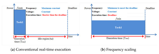
Figure 2.
Real-time execution. (a) Frequency and voltage are set to maximum; hence, the task finishes before deadline. Since frequency and voltage remain constant, power is wasted in the idle region. (b) Frequency scale is set to minimum and remains constant, enabling the task to finish at the deadline, saving power.
A previous study [20] focused on two possible scenarios for executing a given task on an RTS while considering a predefined deadline. In the first scenario, the system works at the minimum frequency at which task execution finishes at the deadline. This means that the minimum and voltages are supplied with a minimum frequency to satisfy the deadline (for example, 10 MHz), as illustrated in Figure 2b. This scenario is our baseline. In the second scenario, shown in Figure 3, the is optimized to boost the frequency in accordance with the alpha power law, so the task is executed in much less time than in the first scenario. This is our test scenario. During the time remaining until the deadline, RBB is applied to reduce the leakage power. If the BB voltage is fixed and the substrate has been charged, almost no current is required for giving the biasing. If the voltage changes dynamically, energy is lost due to substrate charging and discharging.
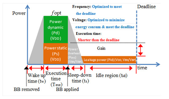
Figure 3.
Case scenario evaluation: Dynamic power management (DPM) with body bias (BB) at maximum frequency. Dynamic and static energies are consumed only during execution. Switching overhead occurs when we apply/remove BB and leakage current occurs in the idle region. Details and characterization of the switching waveform are discussed in a later section.
We previously established a functional mathematical model for power and timing that uses parameters extracted from real chips [6,11]. Moreover, we performed several of the first studies that included energy overhead parameters extracted from real chips [20,21,22]. By using our power and timing model to control BB, we reduced energy consumption by 15.3% at 40 MHz for a deadline of 3 ms and an optimal for the RBB voltage (−500 mV) compared with the baseline. The overhead for dynamic BB switching occupied a considerable part of the total energy required; thus, we had to evaluate the overhead for real chips. Although we identified the optimal point, we used a brute-force coarse-grain search with a limited range of values: From −200 to −700 mV with 100 mV steps for and from 20 MHz to 60 with 10 MHz steps for the frequency [20]. Hence, exploring BB voltages other than the evaluated values was impossible. To overcome these problems, we have now devised a model that includes BB switching overhead, and it is suitable for optimization methodologies.
3. Proposed Energy Consumption and Overhead Calculation Models
3.1. Baseline Model
In our previous work [6,11,20], we developed a power and timing model using BB control. It is based on real-chip measurements of leakage current, switching current, and maximum operating frequency. We measured the target chip at 25 °C. We again assume that the execution time of the target task is fixed and can be estimated, as described in a previous paper [20]. Here, execution time is represented as . The total energy () is the sum of the static energy (), dynamic energy (), energy overhead of the sleep-down transition (), and idle energy ():
This equation can be represented as
where I is the leakage current, A and B are the coefficients of the exponential terms for and , respectively, and is the coefficient of dynamic energy corresponding to the switching activity factor at capacitance C. is the clock cycles per instruction and represents the number of cycles that an instruction needs to be executed; the target system is a V850 E-Star microcontroller (described in Section 5). is the sum of the and energies when we apply BB (Figure 3). Although this paper focuses on for simplicity, the evaluated value includes both energies. Only the sleep-down energy is considered here, since it represents current charging, while the wake-up voltage represents current discharging. The Figure 4 illustrates the device-circuit level connection. We must adjust to the optimal value for each target application and deadline.
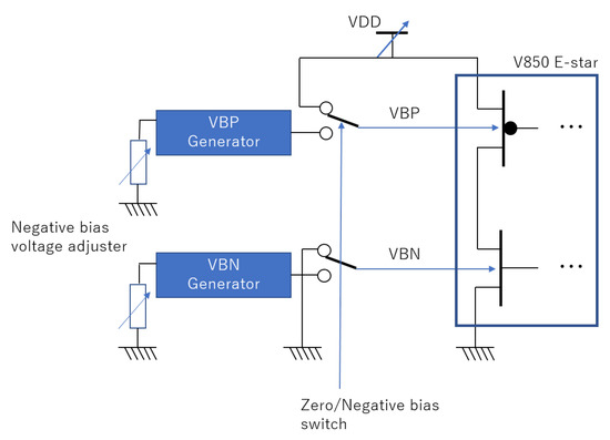
Figure 4.
Device-circuit level connection for the target system: V850 E-star. (supply voltage) is adjusted to the optimal value for each target application and deadline, and not changed during the execution. / (nMOS BB voltage/pMOS BB voltage) are also adjusted to the optimal BB value and switched dynamically to/from zero bias.
Additionally, we must adjust / to the optimal BB value and switch dynamically to/from zero bias. The energy consumed by a / generator itself is not included in . Various types (analog or digital that could work at the near-threshold region) of charge pump circuits/DACs with various tradeoffs have been proposed for VBN/VBP generators [23,24,25,26], and considering the total system including them is beyond the scope of this paper.
As stated above, the execution time for a given task is defined as ; the task is executed with N instructions. The idle time is defined as .
Additionally, should satisfy:
where D is the deadline at which the critical task must be completed, and is the time needed to establish the necessary and when switching to and from active and idle states. can be defined as the sum of the wake-up and sleep-down times, and :
Some of these parameters are obtained from real-chip evaluation, and the others come from the characteristics of the SOTB device. The details of obtaining the parameters were described in our previous paper [20]. However, there was no way to mathematically represent in Equation (2). That is why we could not apply an optimization method to the above expressions. Although there are several models for representing transition behavior [15], they are mostly for controlling the PG supply voltage. Hence, we propose using a double exponential expression, a conventional method in power electronics.
Before going into detail, we show the overall workflow of this study in Figure 5.
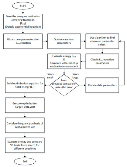
Figure 5.
Overall workflow of the BB control optimization investigation.
3.2. Double Exponential Waveform Expression
We use the double exponential waveform expression to model . We consider an electrical transient to be a temporary disturbance in a power system caused by voltage switching, so a minimal level of transient energy is expected regardless of the circuit. The electrical transients have the shape of a standard full switching impulse (SI) waveform or a double exponential waveform; in our case, this transient occurs after we finish the task execution and we apply BB, as shown in Figure 3. We analyze this transient period from the real chip current measurements.
SI waveforms are characterized by three parameters: The rise time (), which is the time it takes to reach the maximum current amplitude, the current amplitude (,) and the tail time (), that is, the time it takes to settle.
We use these parameters to model to fit into the double exponential waveform [27]. The SI waveform is expressed as
where gamma () and delta () are related to the and times, respectively, and kappa () is the amplitude-modifying factor used to compensate for interaction between the two exponential terms. The factor is related to , and and can be calculated using Equation (6) [28]:
Finally, to get the energy overhead, we need to integrate Equation (5) from time 0 to so that can be expressed as
Furthermore, we assume that changes instantly between constant values. If the voltage source has an inner resistor, the voltage drop must be taken into consideration. Since some charge pump circuits used in VBN controllers have a large inner resistor, it may need to be considered. Here, we assume an ideal battery and a constant / in order to separate the analysis from battery issues.
3.3. Switching Impulse Waveform Model Coefficients
To find appropriate coefficients for the target chip, we use real-chip measurement results with several predefined values of .
The proposed method for modeling is based on known physical parameters, and , and the voltage variation (−200 to −700 mV) that we established from our previous evaluation of an SOTB device [20]. First, we use the Nelder–Mead algorithm to calculate the analytical function parameters of the SI waveform (, , and ) from the known measurements ( and ) of [29]. The following approximations are used to initiate the algorithm:
Next, we calculate with Equation (6) and then Equation (7) using the computed coefficients and evaluate the results by using the mean absolute percentage deviation. Finally, we adjust , , , and as required to optimize the fitting and recalculate . We used this fitting process in each VBN step of our evaluation.
This fitting process is repeated until coefficients are obtained with a minimal error in accordance with the extracted real-chip measurements made in our previous work; for those measurements, we used an SG-4322 function generator to provide BB. Both and were changed simultaneously. The energy and timing overheads were measured using a Keysight MSOX 4104A oscilloscope and N2820A current probe [20]. This process was done to enable comparison of the calculated results with the measured ones and was used as a reference to fine-tune the analytical parameters; that is, real-chip measurement was required only once.
To check the validity of our proposed method, we compare the measured and calculated results in Figure 6 for the worst-case (the largest and smallest of ) evaluation. This fitting process yielded time parameters and with an average error of 10.5%. We present the results of using the model in Table 1. Although the maximum error was about 14%, the impact on the total energy required was about 1.6%, as explained below. This seems to be a reasonable error. The and analytical function parameters were fully evaluated through optimization (Section 4) and through the scenario, as shown in Figure 3 (Section 5). The mean error for these settings is discussed in a later section.
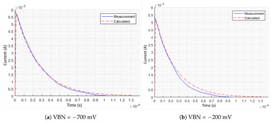
Figure 6.
Comparison of calculated and previously measured current–time profiles for largest and smallest values of : (a) −700 mV; (b) −200 mV.

Table 1.
Energy overhead: Real-chip measurement vs. model analysis results.
4. Optimization
4.1. Problem Definition
There is a tradeoff between power savings and switching overhead. While a high RBB saves a significant amount of static power in the idle state, the switching overhead is larger. Several variables are involved in this tradeoff. Moreover, there is a considerable number of tradeoff possibilities. Let us consider the tradeoff of BB characteristics mentioned in Section 2.1. We control the RBB characteristics by using several electrical parameters concurrently.
More advanced analyses are required to weigh the tradeoffs among all of the variables involved. Therefore, we aim at optimizing selection of the RBB and supply voltage while simultaneously considering the given task deadline, with minimal energy switching penalties and energy waste.
Consistent with the tradeoff information mentioned above, we can describe the problem as a single-objective optimization problem: Given an application, optimize the energy consumption and performance of the given task when there are concurrent options for RBB and the supply voltage.
We use Equation (10) to model this optimization problem. We catalog the variables and coefficients involved into four groups, as summarized in Table 2. The system coefficient variables (I, A, B, , and C) are acquired in accordance with the method described in [6].
Table 2.
Group variables involved in the optimization problem.
Here, the problem is the optimization of energy consumption by finding the optimal and voltages, constrained by the switching overhead penalties and energy waste. This is thus a problem of finding the minimum constrained nonlinear multi-variable equation.
4.2. Interior Point Nonlinear Programming Model
The Newton–Raphson method is commonly applied to engineering problems due to its swift and robust convergence characteristics. Nonetheless, if a given problem has saddles, multiple roots, or the initial condition is not a starting point (since, from a geometrical point of view, selection of the starting point is arbitrary), the algorithm might get caught in a suboptimal solution or may not even converge. It is thus essential that the convergence condition is ensured; therefore, we use a more robust method, the interior point method (IPM). By using the IPM, we can reach and guarantee convergence to the optimum solution by traversing the interior region described by the double exponential waveform rather than around its surface, as done by the Newton–Raphson method. The IPM has been proven to achieve an optimal solution efficiently for these types of optimization problems [30,31].
Its convergence advantage and computational efficiency make IPM an excellent problem-solving method for NLP [31]. Therefore, the objective function is the equation for total energy (Equation (10)) as a function of and . Hence, the optimization problem is
minimize
subject to
The goal is to minimize . To do so, we minimize and in the objective function (Equation (11)) while satisfying the voltage variation constrained for (12) and (13); these constraints are based on our previous analysis of an SOTB device [20]. Another crucial constraint is the frequency, since is related to frequency by the alpha power law; the system must work at a minimum frequency while attaining the performance required to avoid wasting energy. Furthermore, the frequency must be calculated in accordance with its . This relationship is described in the next section. We established an evaluation framework [20] from 20 to 60 MHz with 10 MHz steps and calculated the from this frequency range.
We must ensure that our model complies with the device for its operational time and rising time when applying BB. To demonstrate this, we assume a hypothetical scenario of a 3 ms deadline, which is the independent variable.
We developed a program in MATLAB [32] to compute the objective function with the IPM–NLP algorithm. The target optimization variables for the algorithm are and . We map the coefficients and the formulas to compute the variables of Equation (11). Next, the program calculates the variables and sweeps across the coefficients. For each iteration, the program evaluates each variable with the possible combinations. In this manner, we keep the relationships among variables. It iterates the objective function evaluating and until it converges. The results for our scenario were a of −449 mV and a of 397 mV.
In reality, the and operational frequency are discrete values; however, both have various tradeoffs between cost and accuracy, depending on the available BB generators and clock frequency controllers. Since our method can find a continuous optimal value, we can set the most promising discrete values close to the optimal one in consideration of the available BB generators and clock controllers [23,24,25,26]. We compiled the optimization model with MATLAB R2019a 9.6.0.1174912 on an HP notebook computer (Windows 10 64-bit, Intel i7-8550U CPU 1.8 GHz, RAM 16 GB). The IPM–NLP computation time was 0.474 s.
To evaluate the efficiency of our methods, we estimated the computation time for a brute-force fine-grain search, whereas we used a brute-force coarse-grain search (real-chip measurements) for the evaluation and results. We used a configuration with a voltage variation of −200 to −700 mV with 100 mV steps and a frequency range of 20 to 60 MHz with 10 MHz steps as well as its associated in accordance with the previously reported method [20]. Now, we estimate the computation time for the brute-force fine-grain search. We used the same ranges as for the coarse-grain search but with unit step granularity for each case (, , and frequency) and swept through every combination. The computation time for the search was 4.265 s. Our proposed optimization method outperformed in ≈90% of the brute-force fine-grain search. Moreover, it guarantees an exact optimal solution.
This optimization process is suitable for a compiler or design CAD tools if the execution time of the target program and the deadline are fixed. If they are changed due to a change in requirements, optimization must be done in the run-time system. The execution time of 4.265 s is short enough for optimization to be performed in an edge system. This optimization is needed only when a new task is introduced into the system, which is assumed to happen infrequently and severely influences the energy consumption. Thus, the energy for optimization itself was omitted.
4.3. Optimal Frequency
Once we find the optimal , the next step is to find the optimal frequency f. The gate delay in MOSFETs is expressed using the alpha power law [33]:
where is the process parameter, is the velocity saturation coefficient for the MOSFET, and 1 ≤ ≤ 2 (2 in the case of SOTB technology) [6,33]. The frequency is proportional to the reciprocal of . Therefore, we can determine f by using – optimization:
where F is a coefficient related to frequency and is the threshold voltage, which varies due to the back gate biasing. It can be linearly approximated using:
where is the threshold voltage with ZBB and is a constant given by the technology process coefficient (back gate biasing).
Table 3 summarizes the power model coefficients obtained from real-chip measurements [6]. Using the coefficients in the table in Equation (15), we obtained = 38.02 MHz and = 38.72 MHz for the core and memory, respectively. The variation between and is very small; therefore, as a rule of thumb, we use the slowest one.
Table 3.
Proposed power model coefficients extracted from real-chip measurements.
5. Results and Discussion
5.1. Target System: V850 E-Star
To explore the capabilities of the proposed methodology, we evaluate the break-even time (BET) and optimize the energy for several deadlines. BET is important because, if it exceeds the given deadline, the proposed methodology cannot be used (is not effective). Instead, the device should remain active to cope with the short deadline.
To evaluate the efficiency of the methodology, we used a V850 E-Star microcontroller consisting of a processing unit and a memory module as the target system [34,35,36]. It is a 32 bit RISC microcontroller with a simple in-order five-stage pipeline, 46.2 k gate logic cells, and 128 kb instruction/data memory modules for car electronics developed by Renesas Electronics. The V850 E-Star basically executes one instruction per clock cycle; hence, CPI = 1. The chip is implemented with an LEAP 65 nm FD-SOI SOTB technology node. As mentioned above, the evaluated results include both the and energies.
Additionally, the local memory is the most significant part in the V850 E-Star, because it takes a large part of the leakage power and is also on the critical path. To choose the coefficients to build our model, we consider the memory as the worst-case scenario.
5.2. Break-Even Time
We evaluate the BET using Equation (7), which is the proposed energy overhead calculation model. It is calculated using
where is the static power consumed during the active state and is the power consumed during the idle state. In our previous work [22], we characterized the efficiency of dynamic BB scaling and established the working region of the voltage framework. We set the base of this comparison as the nominal = 600 mV, which is a typical supply voltage for the SOTB used for the V850 E-star. Here, we use this working region as a baseline. For the optimization phase, we use a deadline of 3 ms. Moreover, we use the optimized voltage conditions for and computed using Equation (11). As shown in Figure 7, the BET of the optimized is found at the midpoint of the working region. We obtain 0.28 ms. This is consistent with the 0.25 ms for a −500/−400 mV brute-force search, with ≈10% error.
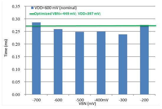
Figure 7.
Break-even time (BET) comparison: Nominal voltage brute-force search vs. optimized – (nominal = 600 m). BET = 0.28 ms for deadline = 3 ms.
5.3. Optimized VBN–VDD
First, we focus on the active state. We set BB at zero bias, and D and are given. The number N of instructions is determined from the baseline scenario with CPI = 1. As mentioned, the V850 E-Star executes one instruction per clock cycle [35,36]. Since the operational frequencies with the settings given above are higher than that of the baseline, the instruction execution of each task finishes prior to the deadline. Furthermore, when a periodic real-time task finishes execution, the system is put into the idle state by the next active state.
We use the optimized voltage conditions for and derived from Equation (11). Additionally, we calculate the optimal frequency from Equation (15). We set the optimized and keep it fixed during the active and idle periods. We do not change it dynamically because this increases the cost.
Next, when the task execution finishes, we put the system into the idle state by applying RBB with the optimized . This creates an electrical transient, which is calculated using Equation (7).
As an example of this optimization, we evaluate the test scenario illustrated in Figure 3 using Equation (10) for a deadline of 3 ms. Figure 8 shows the energy consumption at the optimal and the change in energy consumption with different coarse voltages for different frequencies. The baseline scenario is represented by the dotted line (frequency of 10 MHz). The optimal point of energy reduction, represented by the continuous line, is at 38.06 MHz with an energy consumption of 3.07 J on average, corresponding to 76.22% of the baseline.
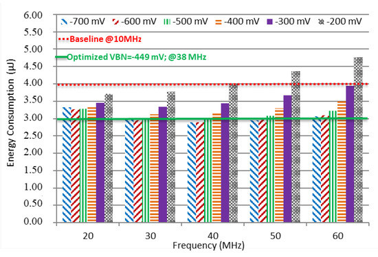
Figure 8.
Total energy consumption including energy transition. Brute-force coarse-grain search vs. optimization IPM–NLP: = 3.07 J, mV, mV, frequency = 38.06 MHz, deadline = 3 ms.
Figure 9 depicts the total energy breakdown by element: , , , and . The graph is grouped by coarse VBN voltages and frequencies. The optimized scenario breakdown energy regions are delimited by horizontal lines. The largest energy reduction is 23.78% for the 38.06 MHz case. These results demonstrate that we can cut the element (from the VBN coarse voltage step) from 20% (−700 mV worst case) or 6% (−200 mV best case) to an optimal 14% of the total energy.
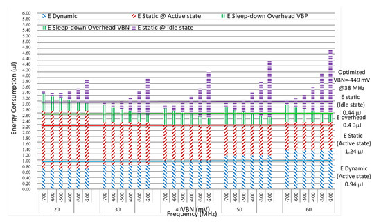
Figure 9.
Total energy breakdown by element, explicitly showing the amount for each element. The with optimized value = −449 mV, = 397 mV shows a cut down to 14%. Deadline = 3 ms.
For further analysis using the same approach used to evaluate the optimized VBN–VDD voltages for a 3 ms deadline (Figure 8), we use this validation approach for deadlines of 2 ms, 3 ms, 4 ms, 12 ms, and 1 s, and use the optimized voltages for and accordingly. As shown in Figure 10, the shorter the deadline, the higher the frequency needed to meet the deadline. The optimized VBN–VDD is on the right side of the graph. The reduction ratios are 18.61%, 23.78%, 26.59%, 32.11%, and 53.19% for 2 ms, 3 ms, 4 ms, 12 ms, and 1 s, respectively. Each reduction ratio is significantly higher than the coarse voltage counterpart. Since the has no significant variation, we can expect that energy reduction is lower for shorter deadlines and higher for longer deadlines. At 1 s, for example, using a lower supply voltage and a lower frequency, it achieves a significant energy reduction. Table 4 summarizes the optimized configurations obtained using interior point nonlinear programming.
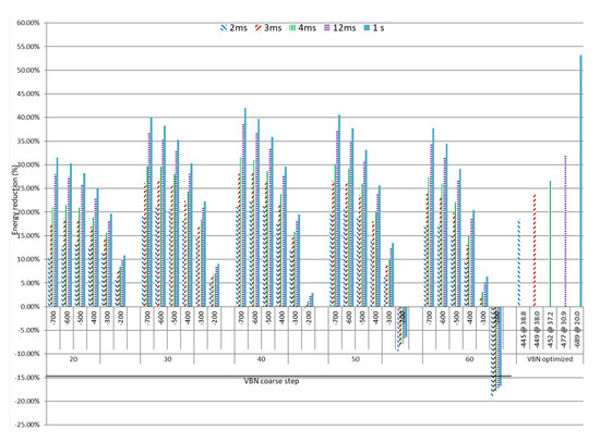
Figure 10.
Energy reduction ratio vs. baseline for deadlines of 2 ms, 3 ms, 4 ms, 12 ms, and 1 s considering leakage current in the idle state and optimal frequency. The shorter the deadline, the higher the frequency needed to meet the deadline.
Table 4.
Supply voltage, reverse body bias (RBB) voltage, and frequency-optimized results by deadline, using interior point nonlinear programming.
5.4. Model Accuracy
The energy overhead calculation model presented in this paper is based on the power and timing model described in Section 3. In Section 3.1, we presented the model for , , and . In Section 3.2 and Section 3.3, we introduced the SI double exponential model, Equation (7). This equation introduces double exponential waveform analytical function parameters (, , and ). These are the fitting parameters for the SI waveform. We use the Nelder–Mead algorithm for its estimation. This is a well-proven algorithm for estimating these parameters. We consider the following errors.
- Mean error. We calculate the error for each VBN coarse voltage, as shown in Table 1. Despite the difference between the real device and the ideal model, the model depicts a close approximation. We achieve a mean error between the analytical model and the real-chip measurement of 10.5%.
- Effect over the model. Although the model uses the time, the error is a function of the VBN voltage. The time duration of changes slightly; however, it does not have a major effect on the waveform. In contrast, the VBN voltage has major changes (every 100 mV); thus, it affects the result. The maximum error is about 14%, whereas the effect on total energy is about 1.6%. Even though the model has a mean error of about 10%, the energy reduction is substantially increased. As we can see in Figure 10, the energy reduction ratio increases from 17.97% to 18.61%, from 21.86% to 23.78%, from 23.81% to 26.59%, from 27.71% to 32.11%, and from 29.64% to 53.19% for 2 ms, 3 ms, 4 ms, 12 ms, and 1 s, respectively, for decreases in the supply voltage, RBB voltage, and frequency. Thus, the effect of the error over the model is negligible.
Additionally, the coefficients of the target device are dependent on the chip temperature. Nevertheless, as in [37], for the FD-SOI SOTB, the coefficients have an accuracy of 93.8% at 25 °C, and at 50 °C, the accuracy is maintained at 91.6%. However, in the worst case, the highest commercial temperature, 65 °C, the accuracy decreases to 79.5%. Thus, the same variations are expected for the proposed model.
6. Conclusions and Future Work
In this paper, we proposed an analytical approach and methodology for optimizing the reverse body bias and supply voltage using interior point nonlinear programming for real-time systems.
We devised an equation for estimating the overhead energy that includes analytical function coefficients. We computed these coefficients using the Nelder–Mead algorithm, thereby transforming the physical parameters of the double exponential waveform into analytical function coefficients. We incorporated this mathematical model into the complete total energy model to improve RTS energy efficiency and accuracy. Then, we used the interior point nonlinear programming model for minimizing the total energy consumption.
The evaluation results demonstrate that the proposed methodology can significantly reduce energy consumption without affecting the system’s ability to meet the task deadline. We analyzed how BB optimization affects energy saving in terms of the tradeoff between energy consumption and execution time. The optimal energy consumption range is from 399 to 375 mV for from 2 to 12 ms and 341 mV for 1 s. For , it is from −445 to −477 mV for the same deadline range and −689 mV for 1 s. This corresponds to frequencies from 38.86 to 30.94 MHz and 20 MHz for 1 s. The results show that the sleep-down transition accounts for 14% of the total energy consumed. We obtained a BET of 0.28 ms, which is consistent with the 0.25 ms of −500 mV/−400 mV brute-force search findings, with ≈10% error.
If the execution time of the target program is severely affected by the inputs and is difficult to estimate, the proposed methodology cannot be applied. However, a number of real-time scheduling algorithms have been reported for programs for which the execution time can be estimated.
Thus, the proposed model can be used as a reference for RTS, automated computation, and for CAD (under development and future work) [38,39]. Extracting the parameters from the real chip was the first step to modeling of all of the SOTB devices. With this model, we can fix the VBN/VBP, VDD, and how much time it should be applied when the target application and the deadline are given. This means that it is useful to design the system, including the chip.
These results demonstrate that the proposed methodology can achieve greater energy reduction, that it increases the accuracy, and that it can be automated.
At the moment of the evaluation, only typical (TT) device dies were available. The future work for this methodology is to validate it across different devices dies (fast-FF and slow-SS) and different device architectures.
Author Contributions
Conceptualization, C.C.C.T. and H.A.; methodology, C.C.C.T.; software, C.C.C.T.; validation, C.C.C.T.; formal analysis, C.C.C.T. and H.A.; investigation, C.C.C.T.; resources, C.C.C.T. and H.A.; data curation, C.C.C.T. and H.A.; writing—original draft preparation, C.C.C.T.; writing—review and editing, C.C.C.T., R.Y. and H.A.; visualization, C.C.C.T. and H.A.; supervision, H.A.; project administration, H.A.; funding acquisition, H.A. All authors have read and agreed to the published version of the manuscript.
Funding
This work was supported by the Ministry of Economy, Trade, and Industry (METI) as part of the “Ultra-Low Voltage Device Project”, by the New Energy and Industrial Technology Development Organization (NEDO), and by the Japanese Society for the Promotion of Science (KAKENHI S Grant 25220002). It was conducted with the assistance of the Keio Science and Technology Research Encouragement Program and the Keio Leading-Edge Laboratory of Science and Technology Program.
Conflicts of Interest
The authors declare no conflict of interest.
References
- Devadas, V.; Aydin, H. DFR-EDF: A Unified Energy Management Framework for Real-Time Systems. In Proceedings of the IEEE Real-Time and Embedded Technology and Applications Symposium, Stockholm, Sweden, 12–15 April 2010; pp. 121–130. [Google Scholar]
- Ikebuchi, D.; Seki, N.; Kojima, Y.; Kamata, M.; Zhao, L.; Amano, H.; Shirai, T.; Koyama, S.; Hashida, T.; Umahashi, Y.; et al. Geyser-1: A MIPS R3000 CPU core with fine grain runtime power gating. In Proceedings of the IEEE Asian Solid-State Circuits Conference, Taipei, Taiwan, 16–18 November 2009; pp. 281–284. [Google Scholar]
- Pillai, P.; Shin, K.G. Real-Time Dynamic Voltage Scaling for Low-Power Embedded Operating Systems. In Proceedings of the Eighteenth ACM Symposium on Operating Systems Principles, Banff, AB, Canada, 21–24 October 2001; pp. 89–102. [Google Scholar]
- Dreslinski, R.G.; Wieckowski, M.; Blaauw, D.; Sylvester, D.; Mudge, T. Near-threshold computing: Reclaiming Moore’s law through energy efficient integrated circuits. Proc. IEEE 2010, 98, 253–266. [Google Scholar] [CrossRef]
- Yan, L.; Luo, J.; Jha, N.K. Joint dynamic voltage scaling and adaptive body biasing for heterogeneous distributed real-time embedded systems. IEEE Trans. Comput. Des. Integr. Circuits Syst. 2005, 24, 1030–1041. [Google Scholar] [CrossRef]
- Okuhara, H.; Kitamori, K.; Fujita, Y.; Usami, K.; Amano, H. An optimal power supply and body bias voltage for a ultra low power micro-controller with silicon on thin box MOSFET. In Proceedings of the IEEE/ACM International Symposium On Low Power Electronics and Design, Rome, Italy, 22–24 July 2015; pp. 207–212. [Google Scholar]
- Ishigaki, T.; Tsuchiya, R.; Morita, Y.; Sugii, N.; Kimura, S.I.; Swart, J.W. Ultralow-power LSI Technology with Silicon on Thin Buried Oxide (SOTB) CMOSFET. In Solid State Circuits Technologies; InTech: London, UK, 2010; pp. 146–156. [Google Scholar]
- Blalock, B.J.; Allen, P.E. Body-driving as low voltage analog design technique for CMOS technology. In Proceedings of the Southwest Symposium on Mixed-Signal Design Iscas, San Diego, CA, USA, 27–29 February 2000; pp. 1–6. [Google Scholar]
- Zhang, K.; Manzawa, Y.; Kobayashi, K. Impact of body bias on soft error tolerance of bulk and Silicon on Thin BOX structure in 65-nm process. In Proceedings of the IEEE International Reliability Physics Symposium, Waikoloa, HI, USA, 1–5 June 2014; pp. 1–4. [Google Scholar]
- Akgul, Y.; Puschini, D.; Lesecq, S.; Beigné, E.; Miro-Panades, I.; Benoit, P.; Torres, L. Power management through DVFS and dynamic body biasing in FD-SOI circuits. In Proceedings of the 51st Annual Design Automation Conference, San Francisco, CA, USA, 1–5 June 2014; pp. 1–6. [Google Scholar]
- Torres, C.C.C.; Okuhara, H.; Ahmed, A.B.; Yamasaki, N.; Amano, H. Analysis of Body Bias Control for Real Time Systems. In Proceedings of the Workshop on Synthesis and System Integration of Mixed Information Technologies, Kyoto, Japan, 24–25 October 2016; pp. 48–53. [Google Scholar]
- Zhou, J.Y.; Boggs, S.A. Low energy single stage high voltage impulse generator. IEEE Trans. Dielectr. Electr. Insul. 2004, 11, 597–603. [Google Scholar] [CrossRef]
- Ueta, G.; Tsuboi, T.; Okabe, S. Evaluation of overshoot rate of lightning impulse withstand voltage test waveform based on new base curve fitting methods-study by assuming waveforms generated in an actual test circuit. IEEE Trans. Dielectr. Electr. Insul. 2010, 17, 1912–1921. [Google Scholar] [CrossRef]
- McConnell, R.A. Amplitude and Energy Spectra of Transient Test Waveforms. In Proceedings of the IEEE EMC International Symposium on Electromagnetic Compatibility, Montreal, QC, Canada, 13–17 August 2001. [Google Scholar]
- Takeda, S.; Miwa, S.; Usami, K.; Nakamura, H. Stepwise Sleep Depth Control for Run-Time Leakage Power Saving. In Proceedings of the great lakes symposium on VLSI, GLSVLSI’12, Boston, MA, USA, 18–20 May 2012. [Google Scholar]
- Cai, H.; Wang, Y.; Naviner, L.A.D.B.; Zhao, W. Robust Ultra-Low Power Non-Volatile Logic-in-Memory Circuits in FD-SOI Technology. IEEE Trans. Circuits Syst. I 2017, 64, 847–857. [Google Scholar] [CrossRef]
- Duarte, D.; Tsai, Y.; Vijaykrishnan, N.; Irwin, M.J. Evaluating run-time techniques for leakage power reduction. In Proceedings of the Asia and South Pacific and the 15th International Conference on VLSI Design, Bangalore, India, 11 January 2002; pp. 31–38. [Google Scholar]
- Keshavarzi, A.; Ma, S.; Narendra, S.; Bloechel, B.; Mistry, K.; Ghani, T.; Borkar, S. Effectiveness of reverse body bias for leakage control in scaled dual Vt CMOS ICs. In Proceedings of the 2001 International Symposium on Low Power Electronics and Design, Huntington Beach, CA, USA, 6–7 August 2001; pp. 207–212. [Google Scholar]
- Tsai, Y.; Duarte, D.E.; Vijaykrishnan, N.; Irwin, M.J. Characterization and modeling of run-time techniques for leakage power reduction. IEEE Trans. Large Scale Integr. Syst. 2004, 12, 1221–1232. [Google Scholar] [CrossRef]
- Torres, C.C.C.; Okuhara, H.; Yamasaki, N.; Amano, H. Analysis of Body Bias Control Using Overhead Conditions for Real Time Systems: A Practical Approach. IEICE Trans. Inf. Syst. 2018, 101, 1116–1125. [Google Scholar] [CrossRef]
- Cortes, C.; Amano, H. Switching Region Analysis for SOTB Technology. In Proceedings of the International Caribbean Conference on Devices, Circuits and Systems, Cozumel, Mexico, 5–7 June 2017; pp. 33–36. [Google Scholar]
- Cortes, C.; Amano, H.; Yamasaki, N. Break Even Time Analysis Using Empirical Overhead Parameters for Embedded Systems on SOTB Technology. In Proceedings of the Design of Circuits and Integrated Systems Conference, Barcelona, Spain, 22–24 November 2017. [Google Scholar]
- Clerc, S.; Saligane, M.; Abouzeid, F.; Cochet, M.; Daveau, J.M.; Bottoni, C.; Bol, D.; De-Vos, J.; Zamora, D.; Coeffic, B.; et al. 8.4 A 0.33V40∘C Process/Temperature Closed-Loop Compensation SoC Embedding All-Digital Clock Multipller and DC-DC Converter Exploiting FDSOI 28nm Back-Gate Biasing. In Proceedings of the International Solid-State Circuits Conference (ISSCC), San Francisco, CA, USA, 22–26 February 2015; pp. 150–151. [Google Scholar]
- Okuhara, H.; Ahmed, A.B.; Amano, H. Digitally Assisted On-Chip Body Bias Tuning Scheme for Ultra Low-Power VLSI systems. IEEE Trans. Circuits Syst. I 2018, 65, 3241–3253. [Google Scholar] [CrossRef]
- Blagojevi, M.; Cochet, M.; Keller, B.; Flatresse, P.; Vladimirescu, A.; Nikolić, B. A Fast, Flexible, Positive and Negative Adaptive Body-Bias Generator in 28nm FDSOI. In Proceedings of the IEEE Symposium on VLSI Circuits, Honolulu, HI, USA, 15–17 June 2016. [Google Scholar] [CrossRef]
- Hoppner, S.; Eisenreich, H.; Walter, D.; Scharfe, A.; Oefelein, A.; Schraut, F.; Oefelein, A.; Schraut, F.; Schreiter, J.; Riedel, T.; et al. Adaptive Body Bias Aware Implementation for Ultra-Low-Voltage Designs in 22FDX Technology. IEEE Trans. Circuits Syst. II Express Briefs 2019. [Google Scholar] [CrossRef]
- Ramarao, G.; Chandrasekaran, K. Calculation of Multistage Impulse Circuit and Its Analytical Function Parameters. Int. J. Pure Appl. Math. 2017, 114, 583–592. [Google Scholar]
- Camp, M.; Garbe, H. Parameter Estimation of Double Exponential Pulses (EMP, UWB) With Least Squares and Nelder Mead Algorithm. IEEE Trans. Electromagn. Compat. 2004, 46, 675–678. [Google Scholar] [CrossRef]
- Nelder, J.; Mead, R. A Simplex Method for Funtion Minimization. Comput. J. 1965, 7, 308–313. [Google Scholar] [CrossRef]
- Rao, B.V.; Kumar, G.N.; Kumari, R.L.; Raju, N.G.S. Optimization of a power system with Interior Point method. In Proceedings of the International Conference on Power and Energy Systems, Chennai, India, 22–24 December 2011. [Google Scholar]
- Yang, X. Engineering Optimization Introduction, An Applications, Metaheuristic; Wiley: Hoboken, NJ, USA, 2010; Chaper 6. [Google Scholar]
- Math Works. MATLAB: The Language of Technical Computing from Math Works; Math Works: Natick, MA, USA, 2018. [Google Scholar]
- Weste, N.H.E.; Harris, D.M. Power in CMOS VLSI Design, 4th ed.; Addison-Wesley-Pearson: Boston, MA, USA, 2011. [Google Scholar]
- Kitamori, K.; Su, H.; Amano, H. Power optimization of a micro-controller with Silicon On Thin Buried Oxide. In Proceedings of the 18th Workshop on Synthesis And System Integration of Mixed Information technologies, Sapporo, Japan, 21–22 October 2013; pp. 68–73. [Google Scholar]
- NEC Corporation. V800 Series Multimedia RISC Microcomputers Pave the Way for System On a Chip, 12th ed.; NEC Corporation: Tokyo, Japan, 2000. [Google Scholar]
- Renesas Electronics Corporation. V850/SC1TM, V850/SC2TM, V850/SC3TM. 32-Bit Single-Chip Microcontrollers. In User’s Manual. RENESAS, 3rd ed.; Renesas Electronics Corporation: Tokyo, Japan, 2010. [Google Scholar]
- Okuhara, H.; Fujita, Y.; Usami, K.; Amano, H. Power Optimization Methodology for Ultralow Power Microcontroller With Silicon on Thin BOX MOSFET. IEEE Trans. Large Scale Integr. (VLSI) Syst. 2017, 25, 1578–1582. [Google Scholar] [CrossRef]
- Krauss, T.A. Planar Electrostatically Doped Reconfigurable Schottky Barrier FDSOI Field-Effect Transistor Structures. Ph.D. Thesis, Technical University of Darmstadt, Darmstadt, Germany, 2017. [Google Scholar]
- PARFAIT: Power-aware AmbipolaR Fpga ArchITecture. Available online: https://www.itiv.kit.edu/english/5497.php (accessed on 10 January 2020).


© 2020 by the authors. Licensee MDPI, Basel, Switzerland. This article is an open access article distributed under the terms and conditions of the Creative Commons Attribution (CC BY) license (http://creativecommons.org/licenses/by/4.0/).