Effect of Cr Doping Concentration on the Structural, Optical, and Electrical Properties of Lead Sulfide (PbS) Nanofilms

Abstract
:1. Introduction
2. Materials and Methods
3. Results and Discussion
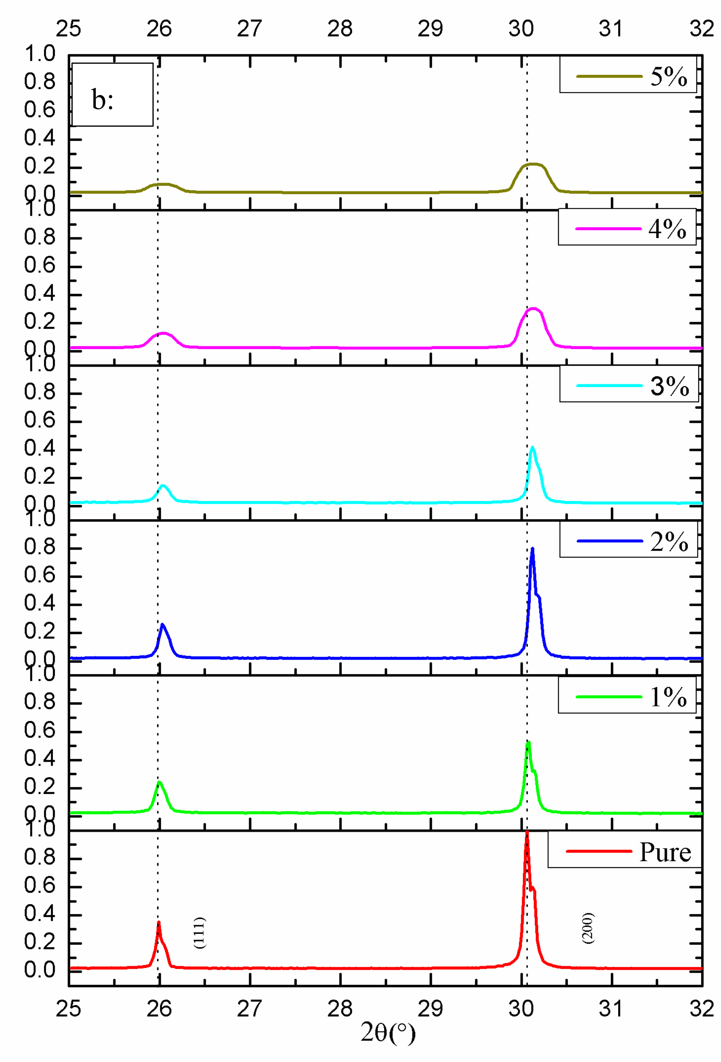
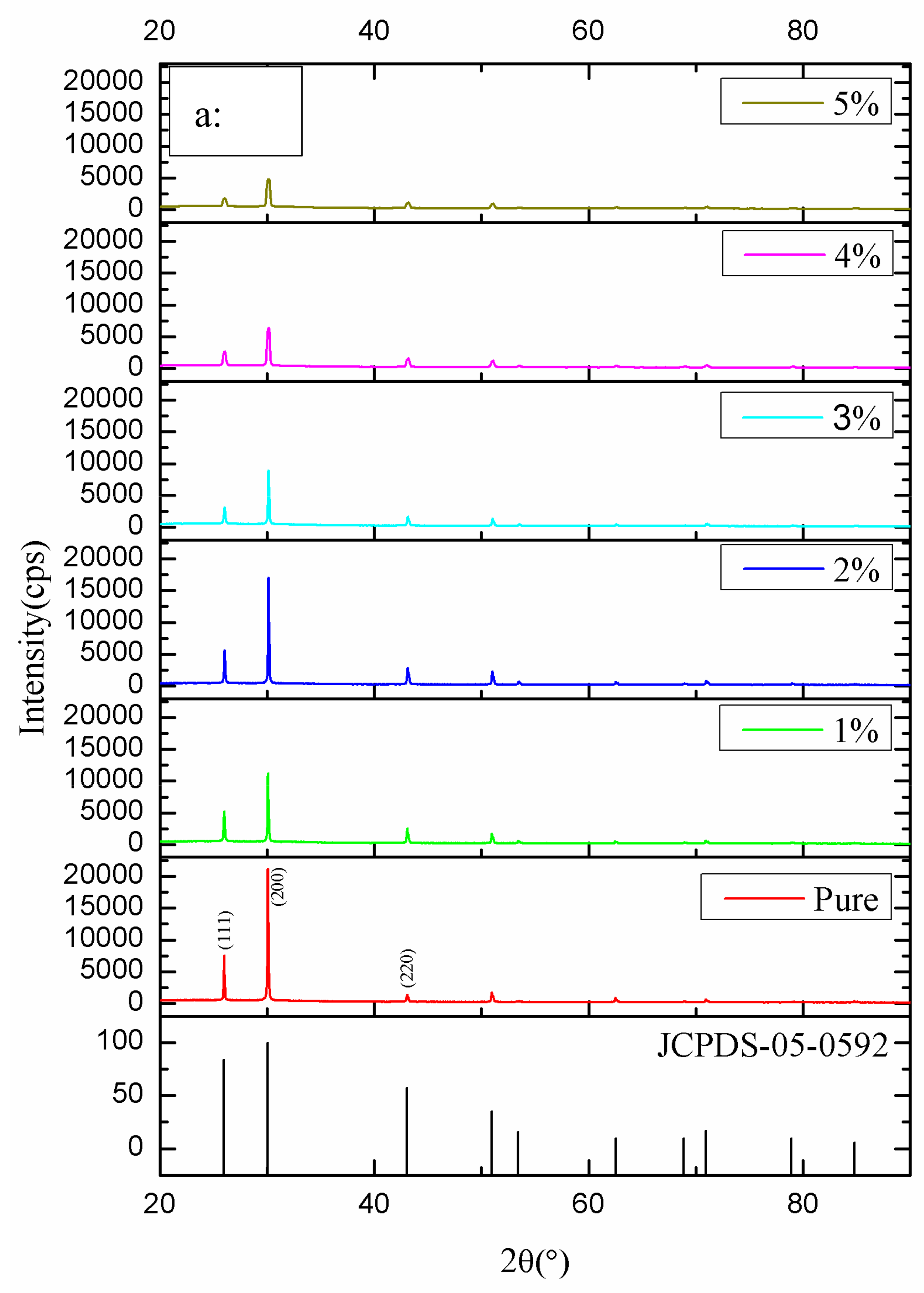
3.1. Structural Properties
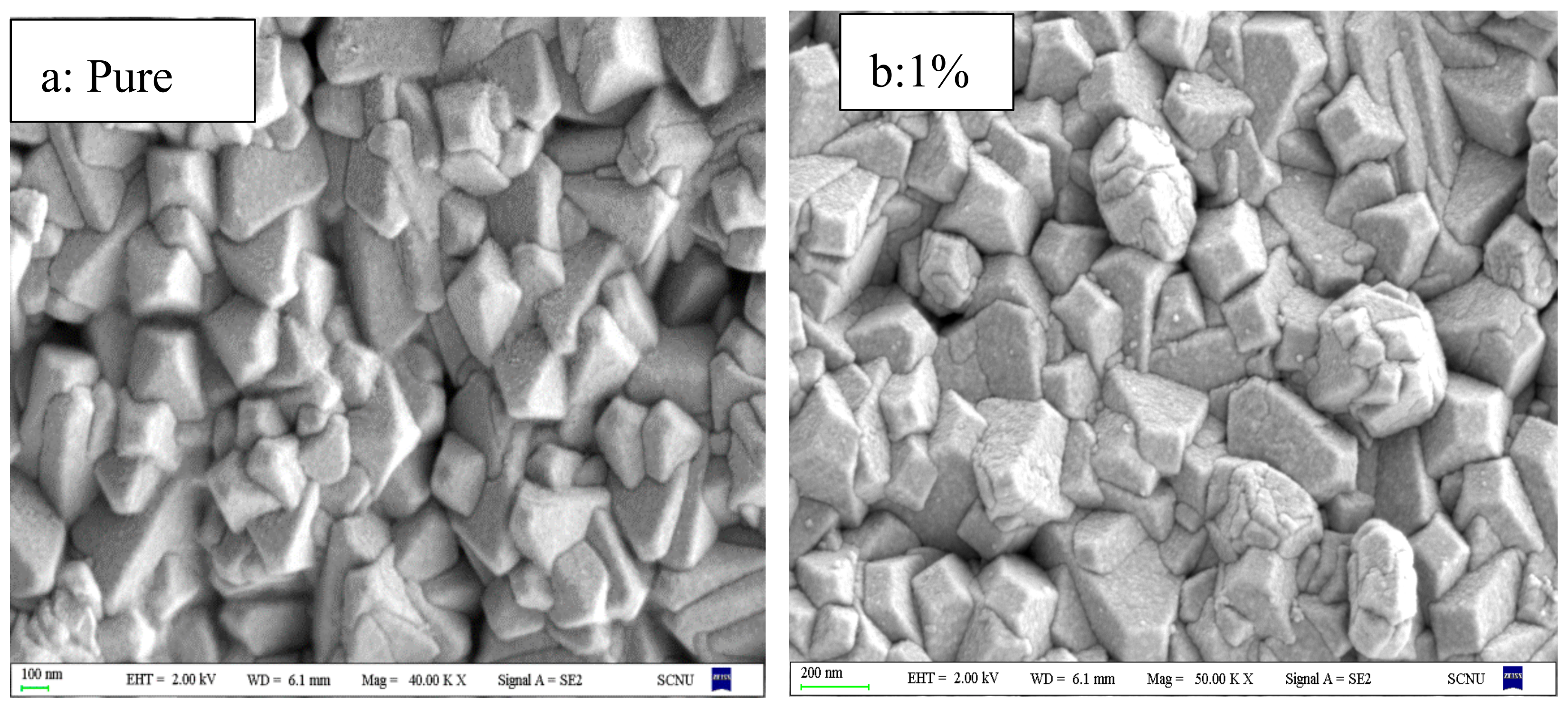
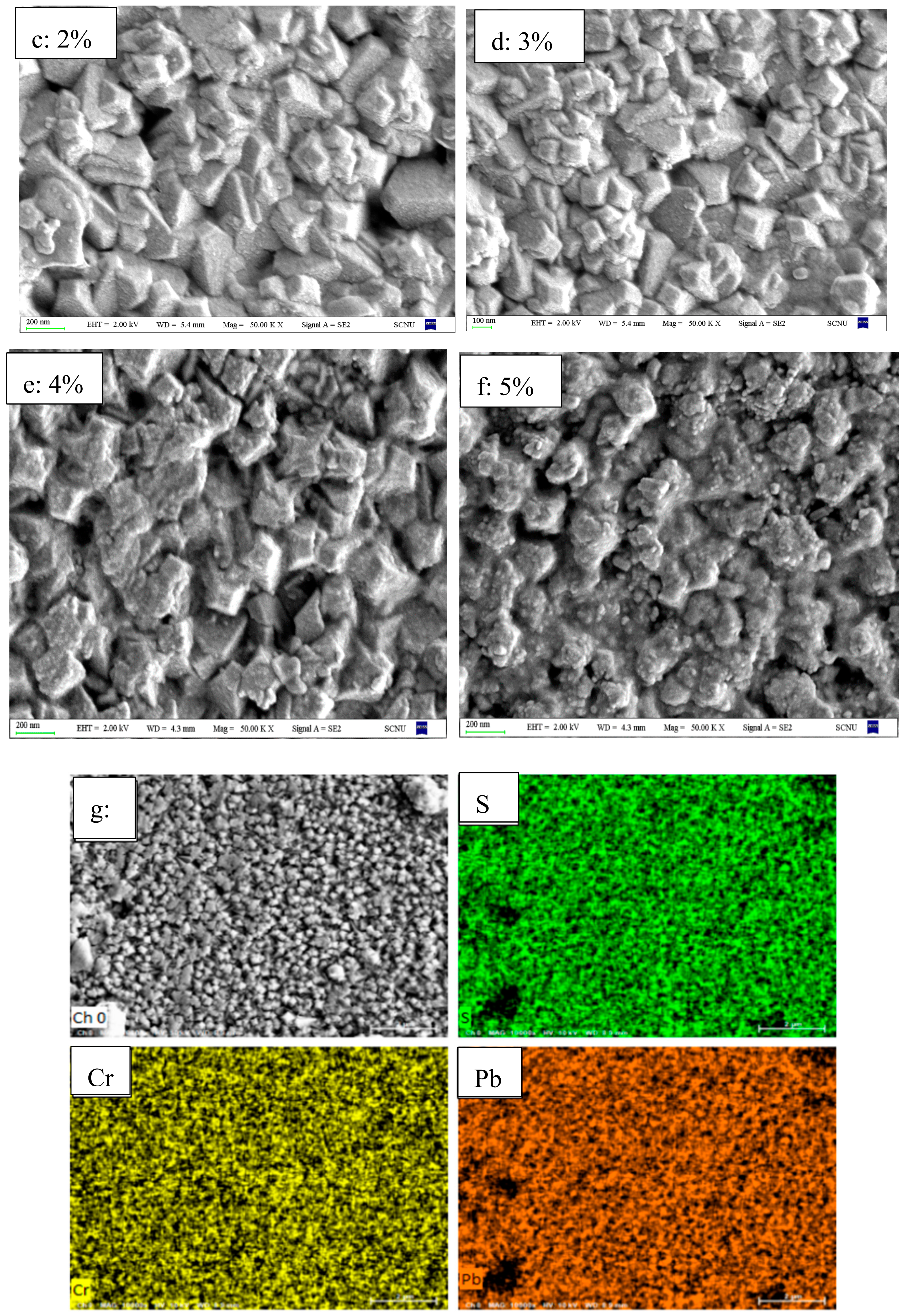
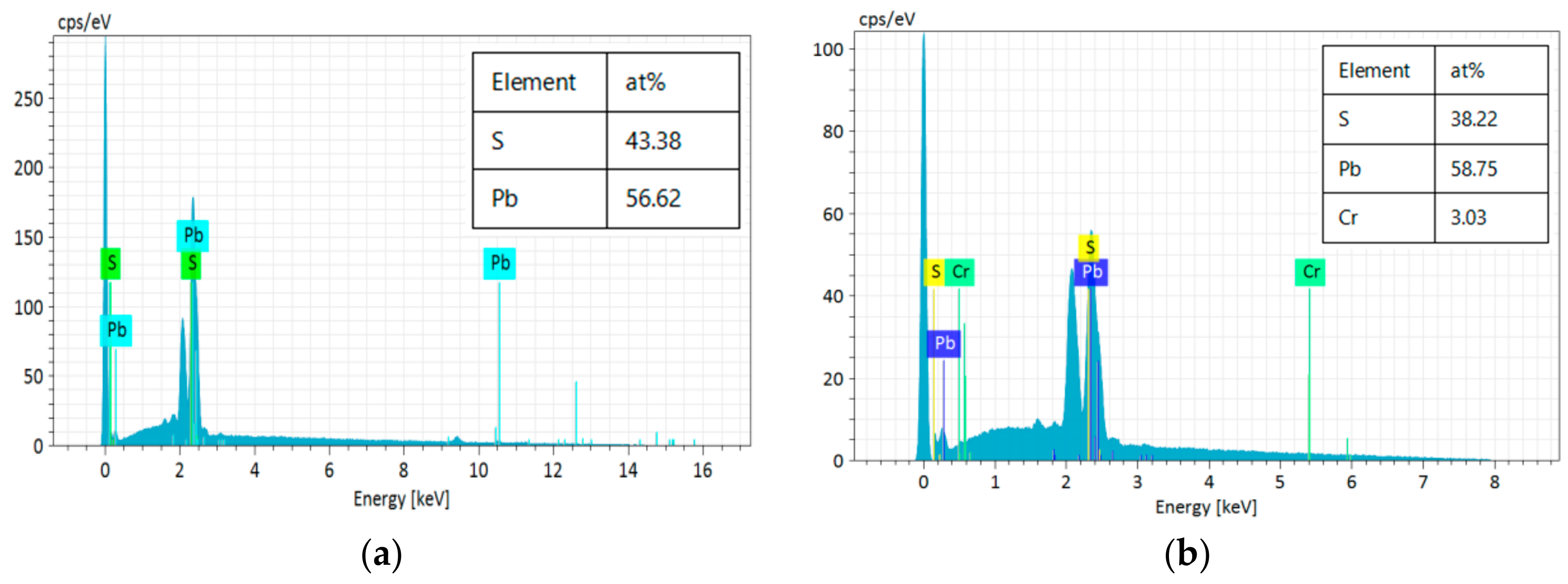
3.2. Morphological Properties
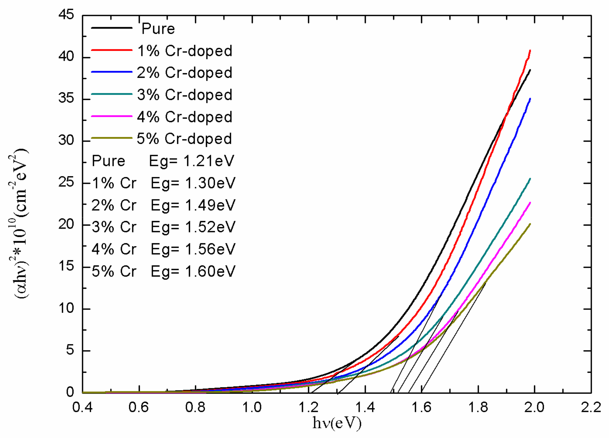
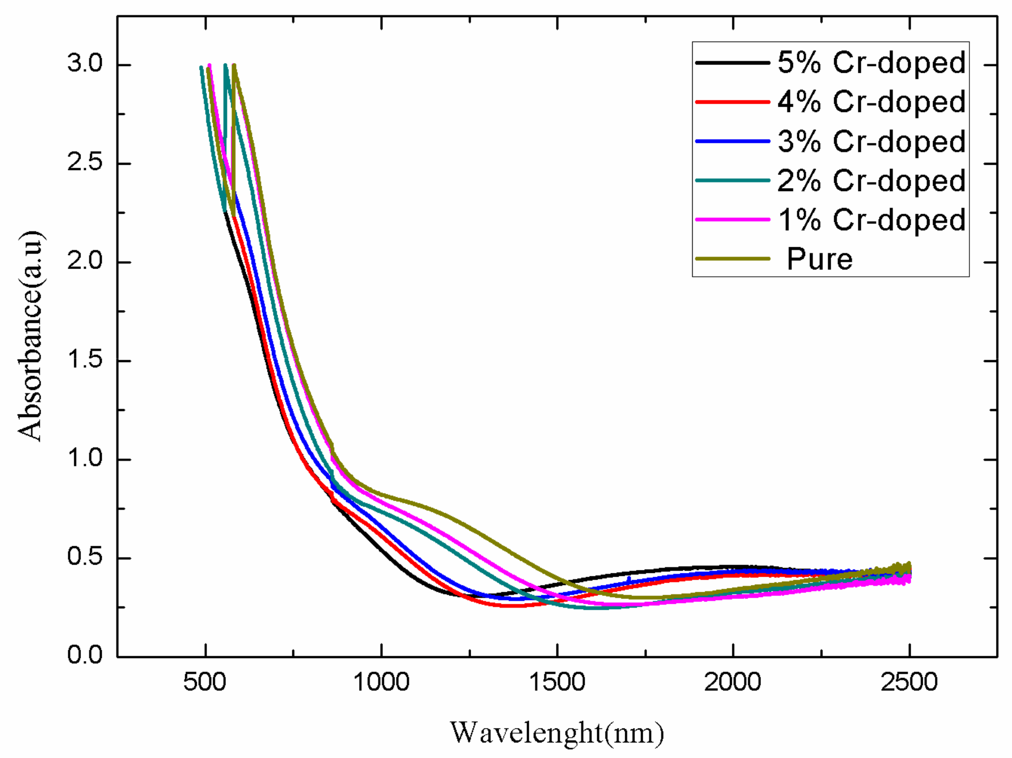
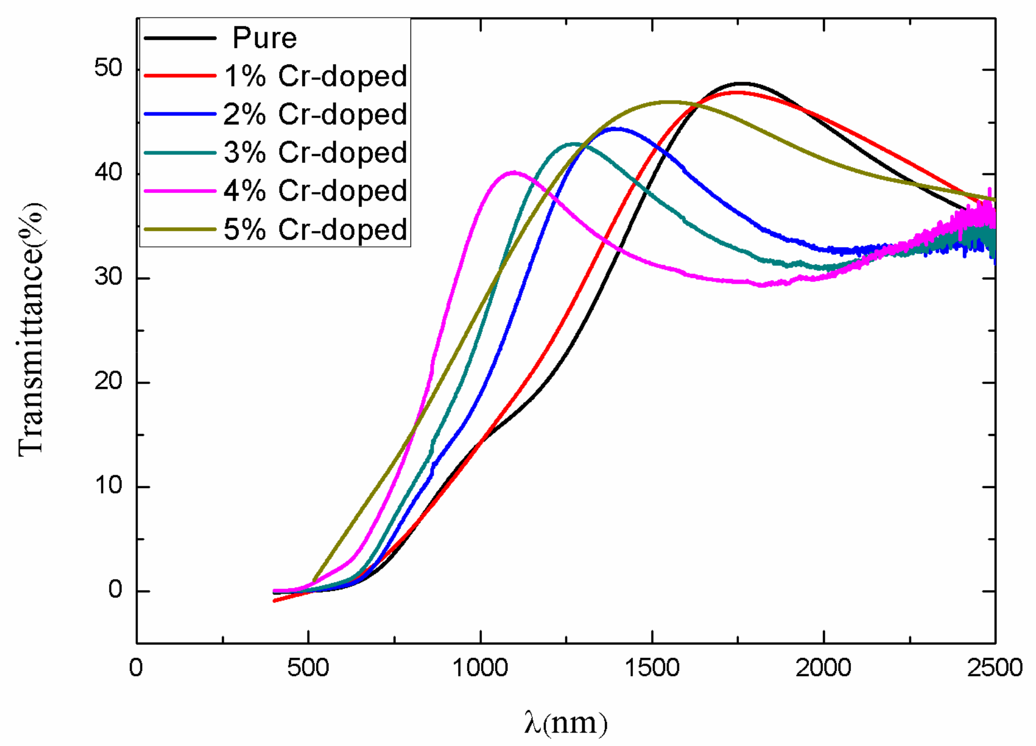
3.3. Optical Research
3.4. Electrical Properties
4. Conclusions
Author Contributions
Funding
Acknowledgments
Conflicts of Interest
References
- Preetha, K.C. Structural, electronic transport and optical properties of Cr doped PbS thin film by chemical bath deposition. In Proceedings of the Let there Be Light: Reflections of a Congress on Light, Kerala, India, 9–11 January 2017. [Google Scholar]
- Gaiduk, A.P.; Gaiduk, P.I.; Larsen, A.N. Chemical bath deposition of PbS nanocrystals: Effect of substrate. Thin Solid Films 2008, 516, 3791–3795. [Google Scholar] [CrossRef]
- Agrahari, V.; Mathpal, M.C.; Kumar, S.; Kumar, M.; Agarwal, A. Cr modified Raman, optical band gap and magnetic properties of SnO2 nanoparticles. J. Mater. Sci. Mater. Electron. 2016, 27, 6020–6029. [Google Scholar] [CrossRef]
- Touati, B.; Gassoumi, A.; Turki, N.K. Structural, optical and electrical properties of Ag doped PbS thin films: Role of Ag concentration. J. Mater. Sci. Mater. Electron. 2017, 28, 18387–18395. [Google Scholar] [CrossRef]
- Touati, B.; Gassoumi, A.; Dobryden, I.; Natile, M.M.; Vomiero, A.; Turki, N.K. Engineering of electronic and optical properties of PbS thin films via Cu doping. Superlattices Microstruct. 2016, 97, 519–528. [Google Scholar] [CrossRef]
- Yücel, E.; Yücel, Y. Fabrication and characterization of Sr-doped PbS thin films grown by CBD. Ceram. Int. 2017, 43, 407–413. [Google Scholar] [CrossRef]
- Yu, K.S.; Shi, J.Y.; Zhang, Z.L.; Liang, Y.M.; Liu, W. Synthesis, characterization, and photocatalysis of ZnO and Er-doped ZnO. J. Nanomater. 2013, 2013, 75. [Google Scholar] [CrossRef]
- Seghaier, S.; Kamoun, N.; Guasch, C.; Zellamac, K. Structural and optical properties of PbS thin films grown by chemical bath deposition. In Proceedings of the Fundamental & Applied Spectroscopy: Second International Spectroscopy Conference, Sousse, Tunisia, 25–28 March 2007. [Google Scholar]
- Preetha, K.C.; Murali, K.V.; Ragina, A.J.; Deepa, K.; Dhanya, A.C.; Remadevi, T.L. The role of cationic precursors in structural, morphological and optical properties of PbS thin films. In Proceedings of the National Seminar on Current Trends in Materials Science, Kerala, India, 4–6 August 2011. [Google Scholar]
- Thangaraju, B.; Kaliannan, P. Spray pyrolytically deposited PbS thin films. Semicond. Sci. Technol. 2000, 15, 849–853. [Google Scholar] [CrossRef]
- Kumar, S.; Sharma, T.P.; Zulfequar, M.; Husain, M. Characterization of vacuum evaporated PbS thin films. Phys. B Phys. Condens. Matter 2003, 325, 8–16. [Google Scholar] [CrossRef]
- Muratore, C. Pulsed laser deposition of thin films, Vol. 2. Plasma Process. Polym. 2010, 4, 847. [Google Scholar] [CrossRef]
- Asavapiriyanont, S.; Chandler, G.K.; Gunawardena, G.A.; Pletcher, D. The electrodeposition of polypyrrole films from aqueous solutions. J. Electroanal. Chem. 1984, 177, 229–244. [Google Scholar] [CrossRef]
- Gümüş, C.; Ulutaş, C.; Esen, R.; Özkendir, O.M.; Ufuktepe, Y. Preparation and characterization of crystalline MnS thin films by chemical bath deposition. Thin Solid Films 2005, 492, 1–5. [Google Scholar] [CrossRef]
- Jana, S.; Thapa, R.; Maity, R.; Chattopadhyay, K.K. Optical and dielectric properties of PVA capped nanocrystalline PbS thin films synthesized by chemical bath deposition. Phys. E Low Dimens. Syst. Nanostruct. 2008, 40, 3121–3126. [Google Scholar] [CrossRef]
- Seghaier, S.; Kamoun, N.; Brini, R.; Amara, A.B. Structural and optical properties of PbS thin films deposited by chemical bath deposition. Mater. Chem. Phys. 2005, 97, 71–80. [Google Scholar] [CrossRef]
- Zheng, X.; Fei, G.; Ji, F.; Wu, H.; Zhang, J.; Hu, X.; Xiang, Y. Cu-doped PbS thin films with low resistivity prepared via chemical bath deposition. Mater. Lett. 2016, 167, 128–130. [Google Scholar] [CrossRef]
- Joshi, R.K.; Sehgal, H.K. Bias-induced changes in carrier type of Pb (1−x) Fe(x)S nanocrystalline solution grown thin films. J. Cryst. Growth 2003, 247, 425–427. [Google Scholar] [CrossRef]
- Mao, H.-Y.; Lo, S.-Y.; Wuu, D.-S.; Wu, B.-R.; Ou, S.-L.; Hsieh, H.-Y.; Horng, R.-H. Hot-wire chemical vapor deposition and characterization of p-type nanocrystalline Si films for thin film photovoltaic applications. Thin Solid Films 2012, 520, 5200–5205. [Google Scholar] [CrossRef]
- Williamson, G.K.; Smallman, R.E. III. Dislocation densities in some annealed and cold-worked metals from measurements on the X-ray debye-scherrer spectrum. Philos. Mag. 1956, 1, 34–46. [Google Scholar] [CrossRef]
- Reddy, T.S.; Kumar, M.C.S. Effect of substrate temperature on the physical properties of co-evaporated Sn2S3 thin films. Ceram. Int. 2016, 42, 12262–12269. [Google Scholar] [CrossRef]
- Yücel, E.; Yücel, Y.; Beleli, B. Optimization of synthesis conditions of PbS thin films grown by chemical bath deposition using response surface methodology. J. Alloy. Compd. 2015, 642, 63–69. [Google Scholar] [CrossRef]
- Portillo, M.C.; Mathew, X.; Santiesteban, H.J.; Castillo, M.P.; Moreno, O.P. Growth and characterization of nanocrystalline PbS:Li thin films. Superlattices Microstruct. 2016, 98, 242–252. [Google Scholar] [CrossRef]
- Rajashree, C.; Balu, A.R.; Nagarethinam, V.S. Enhancement in the physical properties of spray deposited nanostructured ternary PbMgS thin films towards optoelectronic applications. J. Mater. Sci. Mater. Electron. 2016, 27, 5070–5078. [Google Scholar] [CrossRef]
- Sadovnikov, S.I.; Gusev, A.I.; Rempel, A.A. Nanostructured lead sulfide: Synthesis, structure and properties. Russ. Chem. Rev. 2016, 85, 731–758. [Google Scholar] [CrossRef]
- Khot, K.V.; Mali, S.S.; Pawar, N.B.; Mane, R.M.; Kondalkar, V.V.; Ghanwat, V.B.; Patil, P.S.; Hong, C.K.; Kim, J.H.; Heo, J.; et al. Novel synthesis of interconnected nanocubic PbS thin films by facile aqueous chemical route. J. Mater. Sci. Mater. Electron. 2014, 25, 3762–3770. [Google Scholar] [CrossRef]
- Palominomerino, R.; Portillomoreno, O.; Floresgarcía, J.C.; Hernandez-Tecorralco, J.; Martinez-Juarez, J.; Moran-Torres, A.; Rubio-Rosas, E.; Hernandez-Tellez, G.; Gutierrez-Perez, R.; Chaltel-Lima, L.A. PbS nanostructured thin films by in situ Cu-doping. J. Nanosci. Nanotechnol. 2014, 14, 5408–5414. [Google Scholar] [CrossRef]
- Thangavel, S.; Ganesan, S.; Chandramohan, S.; Sudhagar, P.; Kang, Y.S.; Hong, C.-H. Band gap engineering in PbS nanostructured thin films from near-infrared down to visible range by in situ Cd-doping. J. Alloy. Compd. 2010, 495, 234–237. [Google Scholar] [CrossRef]
- Gedi, S.; Reddy, V.R.M.; Kang, J.; Jeon, C.-W. Impact of high temperature and short period annealing on SnS films deposited by E-beam evaporation. Appl. Surf. Sci. 2017, 402, 463–468. [Google Scholar] [CrossRef]
- Choi, H.S.; Jeon, S.; Kim, H.; Shin, J.; Kim, C.; Chung, U.-I. The impact of active layer thickness on low-frequency noise characteristics in InZnO thin-film transistors with high mobility. Appl. Phys. Lett. 2012, 100, 173501. [Google Scholar] [CrossRef]


| Cr Content (at.%) | (hkl) | 2θ (°) | FWHM (radian) | Crystallite Size D (nm) | Microstrain (ε) × 10−3 | Dislocation Density (ρ) | d-Values (Ä) | Lattice Parameter (Ä) |
|---|---|---|---|---|---|---|---|---|
| 0 | 111 | 25.971 | 0.002234 | 63.7 | 0.544 | 2.47 | 3.42797 | 5.93742 |
| 200 | 30.06 | 0.002007 | 71.5 | 0.485 | 1.95 | 2.97033 | 5.94066 | |
| 220 | 43.081 | 0.003176 | 46.9 | 0.739 | 4.54 | 2.09795 | 5.93389 | |
| 1 | 111 | 26.02 | 0.002374 | 60 | 0.578 | 2.78 | 3.42162 | 5.92643 |
| 200 | 30.081 | 0.002496 | 57.5 | 0.603 | 3.02 | 2.9683 | 5.93661 | |
| 220 | 43.081 | 0.004868 | 20.6 | 1.132 | 10.067 | 2.09795 | 5.93389 | |
| 2 | 111 | 26.026 | 0.002688 | 52.9 | 0.655 | 3.57 | 3.42085 | 5.92509 |
| 200 | 30.124 | 0.002618 | 54.8 | 0.632 | 3.32 | 2.96416 | 5.92833 | |
| 220 | 43.124 | 0.005236 | 18.5 | 1.217 | 12.34 | 2.09596 | 5.92826 | |
| 3 | 111 | 26.033 | 0.004869 | 29.2 | 1.186 | 11.71 | 3.41995 | 5.92352 |
| 200 | 30.126 | 0.00356 | 40.3 | 0.86 | 6.15 | 2.96397 | 5.92794 | |
| 220 | 43.129 | 0.005236 | 18.3 | 1.217 | 12.33 | 2.09572 | 5.9276 | |
| 4 | 111 | 26.042 | 0.007121 | 20 | 1.734 | 25.04 | 3.41878 | 5.92151 |
| 200 | 30.142 | 0.005236 | 27.4 | 1.264 | 13.3 | 2.96244 | 5.92487 | |
| 220 | 43.143 | 0.008238 | 18.1 | 1.915 | 30.53 | 2.09508 | 5.92577 | |
| 5 | 111 | 26.045 | 0.009023 | 15.8 | 2.198 | 40.2 | 3.4184 | 5.92084 |
| 200 | 30.167 | 0.00765 | 18.9 | 1.538 | 19.68 | 2.96004 | 5.92007 | |
| 220 | 43.145 | 0.009372 | 15.9 | 2.179 | 39.52 | 2.09498 | 5.92551 |
| Cr Content (at.%) | Resistivity (10−1 Ω∙cm) | Hall Mobility µ (cm2∙V−1∙s−1) | Volume Carrier Concentration (1016 cm−3) |
|---|---|---|---|
| 0 | 3.47 | 8.27 | 3.70 |
| 1 | 2.95 | 11.9 | 6.86 |
| 2 | 1.23 | 59.6 | 20.7 |
| 3 | 5.43 | 6.18 | 1.53 |
| 4 | 6.9 | 3.9 | 0.659 |
| 5 | 13.2 | 2.15 | 0.304 |
© 2019 by the authors. Licensee MDPI, Basel, Switzerland. This article is an open access article distributed under the terms and conditions of the Creative Commons Attribution (CC BY) license (http://creativecommons.org/licenses/by/4.0/).
Share and Cite
Huo, J.; Li, W.; Wang, T. Effect of Cr Doping Concentration on the Structural, Optical, and Electrical Properties of Lead Sulfide (PbS) Nanofilms. Coatings 2019, 9, 376. https://doi.org/10.3390/coatings9060376
Huo J, Li W, Wang T. Effect of Cr Doping Concentration on the Structural, Optical, and Electrical Properties of Lead Sulfide (PbS) Nanofilms. Coatings. 2019; 9(6):376. https://doi.org/10.3390/coatings9060376
Chicago/Turabian StyleHuo, Jiabin, Wei Li, and Teng Wang. 2019. "Effect of Cr Doping Concentration on the Structural, Optical, and Electrical Properties of Lead Sulfide (PbS) Nanofilms" Coatings 9, no. 6: 376. https://doi.org/10.3390/coatings9060376
APA StyleHuo, J., Li, W., & Wang, T. (2019). Effect of Cr Doping Concentration on the Structural, Optical, and Electrical Properties of Lead Sulfide (PbS) Nanofilms. Coatings, 9(6), 376. https://doi.org/10.3390/coatings9060376