1. Introduction
Aluminum antimony (AlSb) is a binary compound semiconductor material with a theoretical indirect band gap of 1.62 eV that is very compatible with the solar spectrum [
1]. Due to the proper band gap and high carrier mobility, AlSb has wide applications in anode materials for Li-ion battery, PN junction diodes, transistors, room temperature radiation detection, room temperature gamma ray detection, photovoltaic conversion devices, and so on [
2,
3,
4]. As a potential absorption material, the theoretical photoelectric conversion efficiency of AlSb based solar cells is up to 27%, which has recently drawn extensive attention [
5,
6].
It is well known that some methods have been used to prepare AlSb, such as bulk AlSb crystals that were prepared by the Czochralski method [
7,
8]. AlSb thin films were deposited by sputtering [
9], evaporation [
10], electrodeposition [
4], hot wall epitaxy [
11], molecular beam epitaxy (MBE) [
2,
12], metal organic chemical vapor deposition (MOCVD) [
13], and pulsed laser deposition (PLD) [
14]. Previously we have successfully prepared AlSb thin films based on our facile PLD method [
15]. However, Al and Sb ions can easily react with air and moisture. Recently, theoretical calculations predict Zn doping can dramatically increase the chemical stability and reduce the band gap for AlSb thin films [
16]. Meanwhile, experimental element doping of AlSb while the thin film is formed is still in its infancy. In this paper, we demonstrated the preparation of Zn-doped AlSb thin films by the one-step facile PLD method. The optical and electrical properties of the films have been studied. An AlSb-based photovoltaic device was fabricated, from which we observed an obvious photovoltaic effect.
2. Experimental
A KrF excimer laser (Lambda Physik Compex 201, Dieburg, Germany, λ = 248 nm, pulse duration = 20 ns) was employed to fabricate AlSb:Zn thin films on glass substrates by the PLD method. A pulse energy of 110 mJ with a laser repetition rate of 6 Hz was pulsed on a single source of AlSb target. This was mixed with 0.1 at.% Zinc (purity 99.99% atomic percentage) and used to grow AlSb:Zn thin films. The background vacuum was set as lower than 1.5 × 10⁻³ Pa (the ultimate vacuum of the PLD system) during the entire deposition process. For the very low deposition rate at higher deposition pressure, the lowest vacuum in the experiment was necessary. The films with few pinholes were obtained under these parameters. During the growth, the glass substrates were kept hot, so the substrate temperatures varied in the range of 300 °C to 400 °C. The films were amorphous below 300 °C and it was difficult to prepare AlSb:Zn films above 400 °C due to re-evaporation in the PLD system. Finally, all the samples naturally cooled down to room temperature in the vacuum chamber. The thickness of AlSb:Zn thin films was about 400 nm.
The optical transmittance of AlSb:Zn thin films was measured by ultraviolet-visible spectroscopy (Perkin Elmer Lambda 950, Waltham, MA, USA). The X-ray diffraction (XRD) spectra for structure analysis were measured by DanDong Hao Yuan DX-2700, Dandong, China, using Cu Kα radiation (λ = 1.5405 Å). The film thickness was examined by a probe surface profiler (Ambios Technology XP-2, Santa Cruz, CA, USA). The scanning electron microscopy (SEM) images of AlSb:Zn thin films were obtained by HITACHI S5200 (Tokyo, Japan). A Labram HR Evolution Raman spectrometer (Horiba, Kyoto, Japan) with a 532 nm Argon laser was used to characterize the Raman spectra of the films. The valence band spectrum was carried out by using an X-ray photoelectron spectrometer (XPS, THERMO FISHER ESCALAB-250Xi, Waltham, MA, USA).
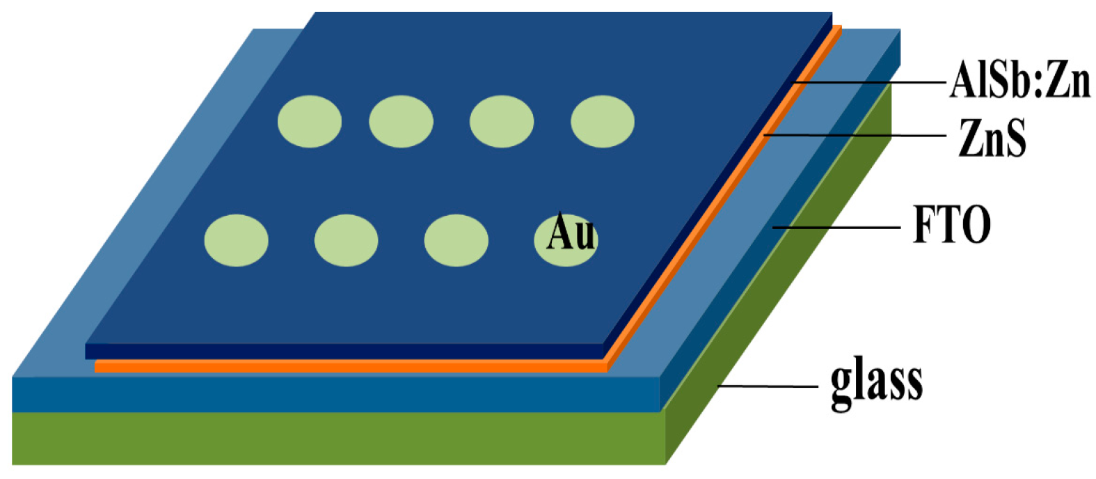
Based on the above studies, the FTO/ZnS/AlSb:Zn/Au device was fabricated and an obvious photovoltaic effect was observed in the device.
Figure 1 depicts the structure of an AlSb-based solar cell, in which both the ZnS thin film (~200 nm) and the AlSb:Zn thin film (~1 µm) were deposited by the PLD method. The Au electrode (~100 nm) was prepared by vacuum evaporation. The ZnS thin film was deposited at the substrate temperature of 200 °C by the PLD method [
17,
18]. A pulse energy of 110 mJ with a laser repetition rate of 6 Hz was applied for the growth of the ZnS thin films. The distance between the target and the substrate was 4 cm. The deposition rate of ZnS was 15 nm/min. As an absorber layer, the AlSb:Zn thin film should be thicker than the 400 nm of the thin film samples. The FTO was the commercial SnO
2:F thin film (~500 nm), with a sheet resistance of 15 Ω/□. The area of the unit cell was 0.0707 cm
2. The open circuit voltage was measured by a multimeter under an AM 1.5 illumination at room temperature.
3. Results and Discussion
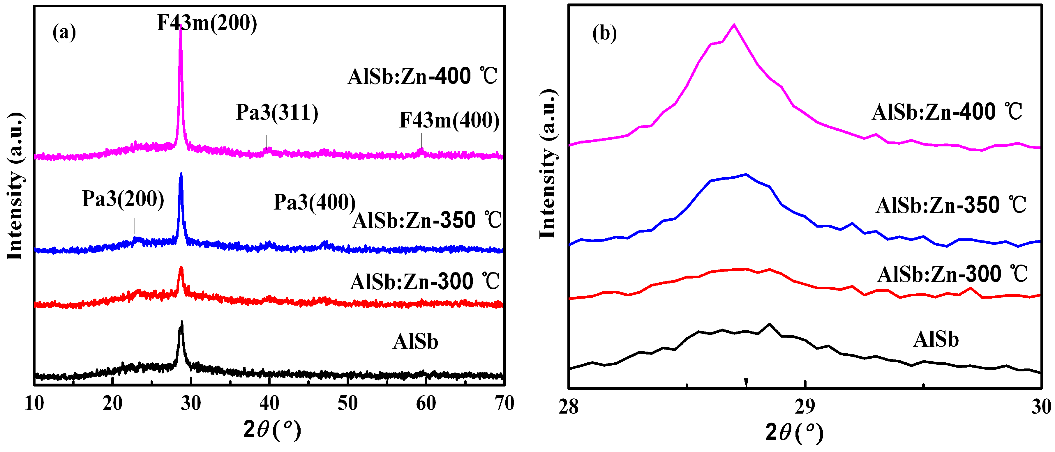
The full scale XRD patterns of AlSb:Zn thin films deposited at different temperatures are shown in
Figure 2a. There were two or more diffraction peaks with cubic structure for all the AlSb:Zn films, indicating that all the films were polycrystalline. Two space groups, F43m and P3a, of AlSb are observed in
Figure 2a. Polycrystalline AlSb:Zn films exhibited a preferred (200) orientation of space group F43m. At lower substrate temperatures, there was (200) plane of space group F43m and (200), (311), and (400) planes of space group Pa3. However, another diffraction peak of (400) plane of space group F43m was observed at 400 °C. Meanwhile, the intensity of main diffraction peak increased sharply as the substrate temperature increased from 300 °C to 400 °C, which indicated that the crystallization of the AlSb:Zn thin film was enhanced when the substrate temperatures were elevated. High substrate temperature is very important for obtaining crystal AlSb:Zn films during the whole deposition process. The higher substrate temperature may help the growing species to obtain a higher mobility. Therefore it may promote the lateral growth of the AlSb:Zn thin films.
Figure 2 shows the enlarged scale (28°–30°) of the XRD patterns. Compared with the XRD of undoped AlSb film, the diffraction peaks of all the AlSb:Zn films had a little left shift. Due to the Zn doping in AlSb:Zn structure, Zn atoms would substitute Al atoms resulting excess holes. AlSb films doped Zn were P-type materials. Due to differences in atomic radius sizes of Al and Zn atoms, the residual strain of the films was originated from atomic size differences, thus the diffraction peak had a shift for Zn-doping.
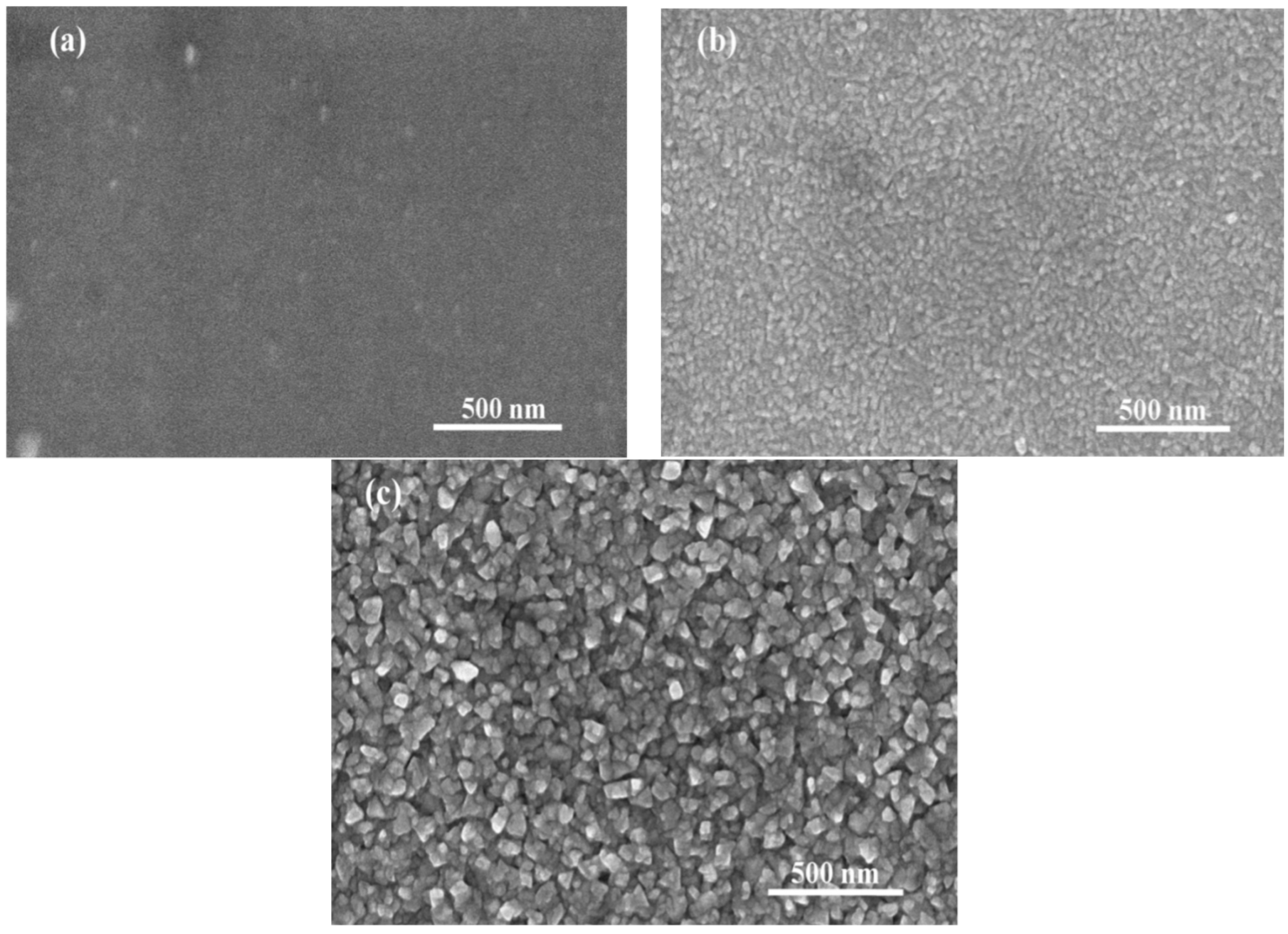
The surface morphology properties are very important for solar cells and other devices because of their effect on the interface among different film layers. The SEM images of AlSb:Zn thin films were shown in
Figure 3. Obvious grains were observed at the higher substrate temperatures (350 and 400 °C) while no grains could be seen at the lower substrate temperature (300 °C), which was in accordance with the XRD results. Moreover, as the substrate temperature increased, the grain sizes became bigger. When the substrate temperature reached 400 °C, the smallest grain sizes were ~20 nm and the biggest grain sizes were ~100 nm by using the scale bar. The big grain size was helpful for the carrier transportation in AlSb-based solar cells.
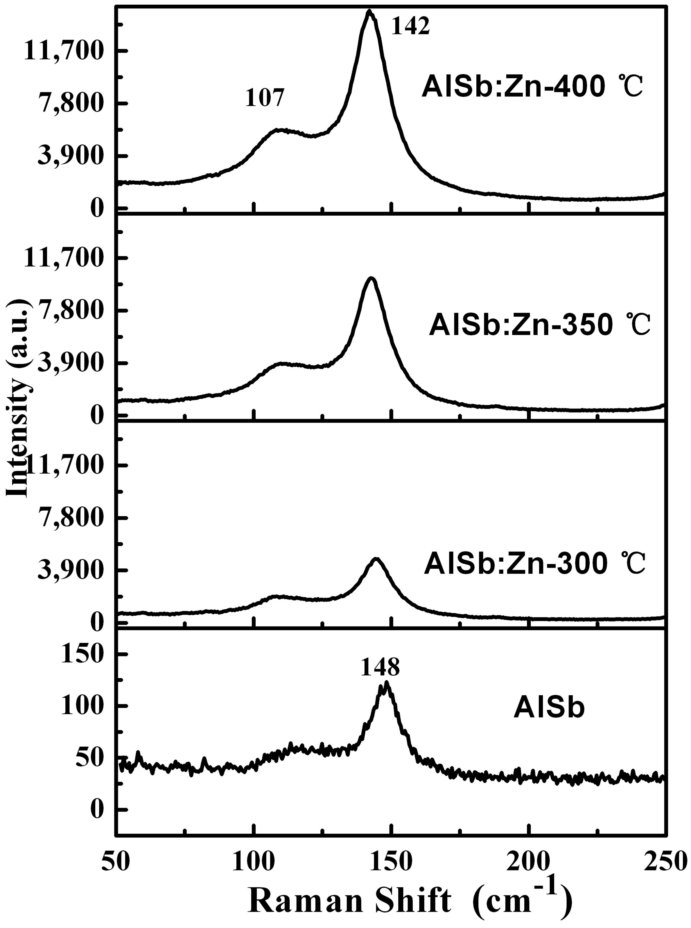
Figure 4 showed the Raman spectra of AlSb:Zn thin films recorded in the wide range of 50–230 cm
−1. The Raman profiles of all the AlSb:Zn thin films were similar and the Raman peaks appeared in the same position located at ~107 and ~142 cm
−1, which revealed similar variations existing in the AlSb:Zn thin film structures. The intensity of the Raman peaks improved as the substrate temperature increased from 300 °C to 400 °C. The improved intensity of the Raman spectra could be attributed to the increased crystallinity of the films. The scattering energy consumption was larger for the poor crystallinity and made the intensity of Raman peak decrease. The dominated Raman peak was at ~142 cm
−1, which was close to the LO peak for bulk AlSb (~150 cm
−1). It can be noted that one peak observed, located at ~107 cm
−1, was similar to the Raman spectra of AlSb thin films deposited by the PLD method by Das et al. [
14]. Compared with the AlSb thin films, the Raman peak positions had a left shift. It is known that the shift of Raman peaks can be attributed to residual stress, structural disorder, doping, and crystal defect in the films. When Zn atoms substituted Al atoms, the crystal lattice of AlSb would have changed for the different atomic radius sizes of Al and Zn atoms, causing the AlSb crystal lattice to be distorted. Thus, the crystal lattice distortion appeared as a shift in Raman spectrum [
19,
20]. Approximately the same Raman shift indicated similar structural stress among the three AlSb:Zn thin films [
21]. Meanwhile, the same Raman shift peaks revealed similar structures among the AlSb:Zn thin films.
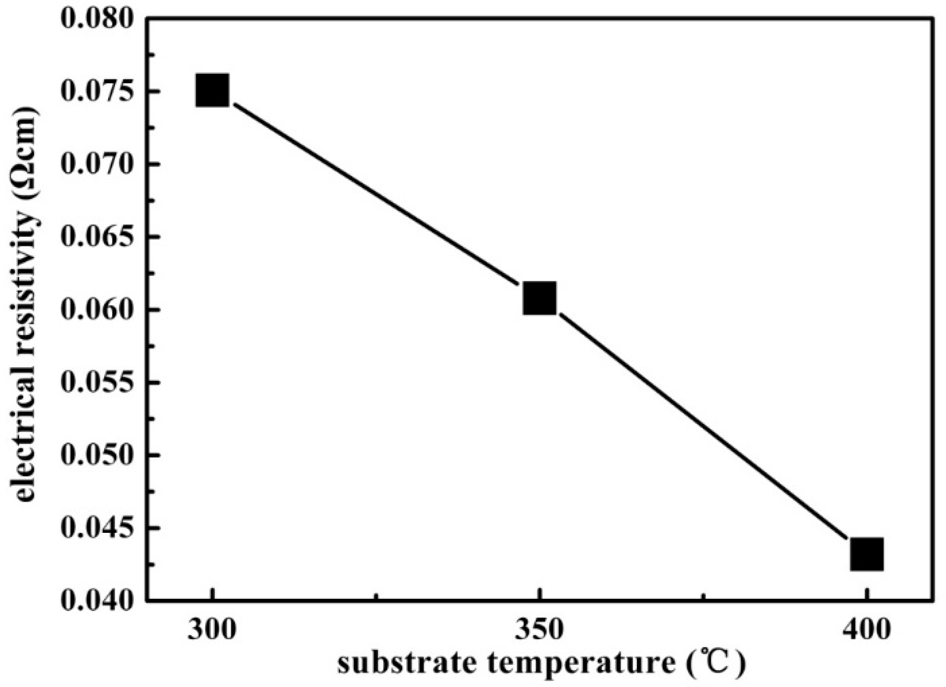
The electrical resistivity of AlSb:Zn thin films is shown in
Figure 5. The electrical resistivity of the AlSb:Zn thin films gradually decreased from 7.5 × 10
−2 to 4.3 × 10
−2 Ω·cm as the substrate temperature increased. The electrical resistivity of the AlSb:Zn thin films was lower at the higher substrate temperature for the bigger grain size, reducing the grain boundary scattering.
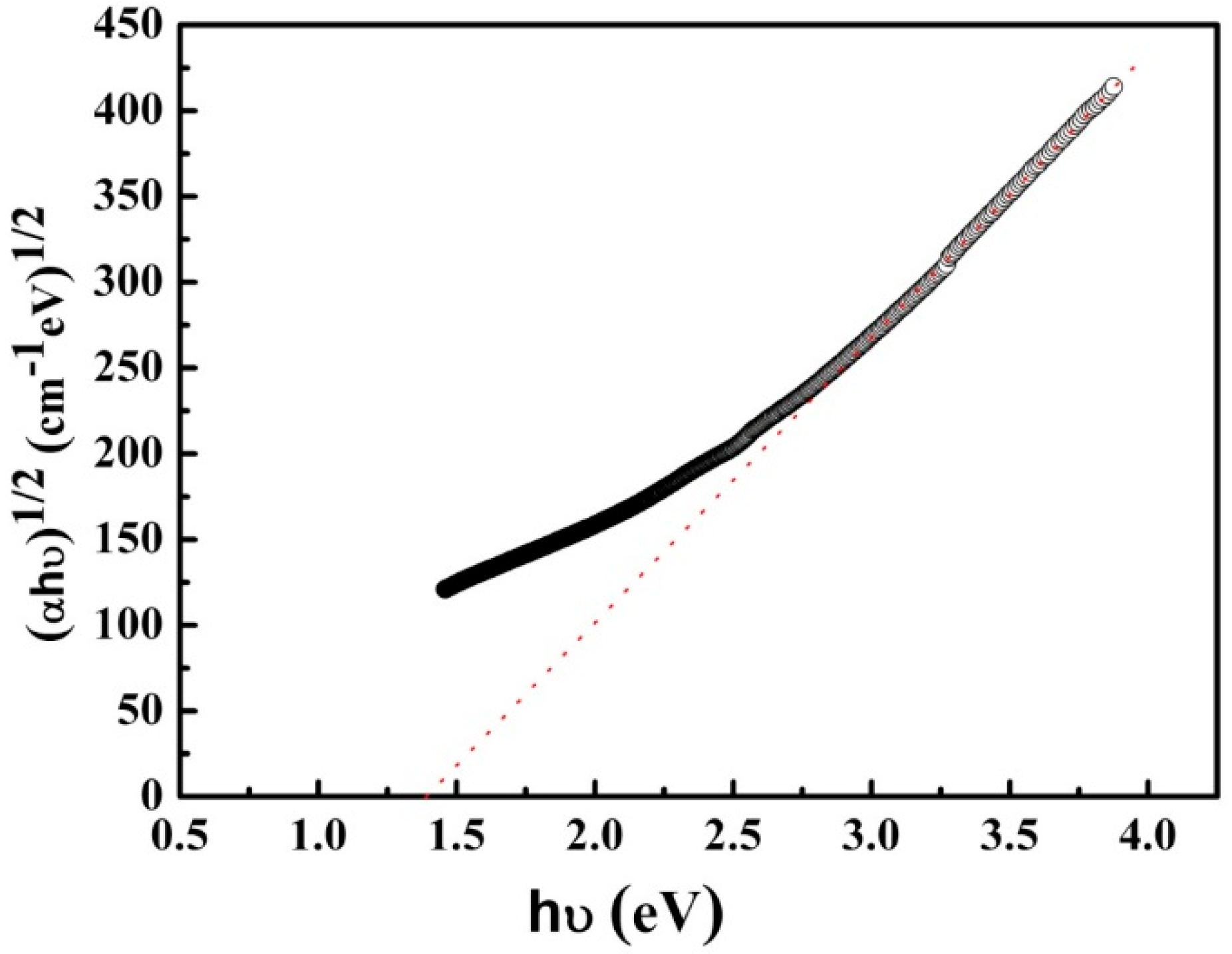
The optical transmittance spectra of all the AlSb:Zn thin films were obtained by ultraviolet-visible spectroscopy (not shown here). The absorption coefficient α can be calculated from the transmittance spectra. The indirect band gap material is subject to the following relationship [
11]:
where A is a constant,
hν is the photon energy, and
Eg is the optical band gap. The plot of (α
hν)
1/2 versus
hν profile of a representative AlSb:Zn film deposited at 400 °C was given in
Figure 6. The extrapolation of the straight line to (α
hν)
1/2 = 0 axis gives the value of
Eg. A band gap of 1.4 eV was obtained, which was lower than the theoretical band gap of AlSb. The valence band maximum of AlSb moved to the high energy zone, while the conduction band minimum moved to the lower zone for the Zn doping, thus the band gap became smaller. As a potential absorber layer of solar cells, the decreased band gap is beneficial for the light absorption in the long wavelengths.
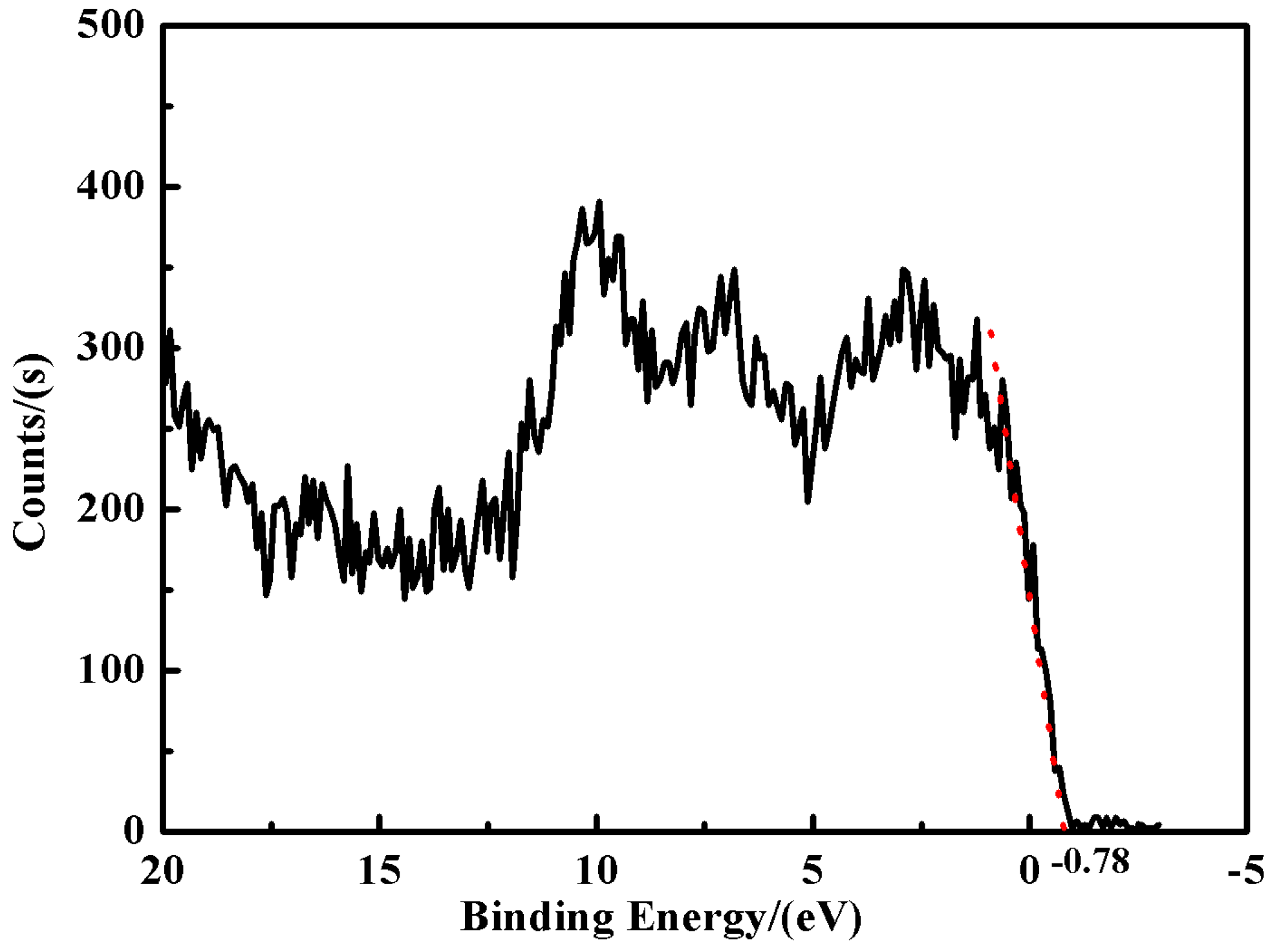
The valence band spectrum of a representative AlSb:Zn film deposited at 400 °C was carried out by XPS.
Figure 7 shows the valence band spectrum of the film. The valence band maximum was determined by an extrapolation of a line fit to the leading edge of the spectrum. The valence band maximum was −0.78 eV for the AlSb:Zn film, which means the Fermi level was below the valence band maximum and the AlSb:Zn films were P-type materials. Zn doping changed the energy band structure of AlSb.
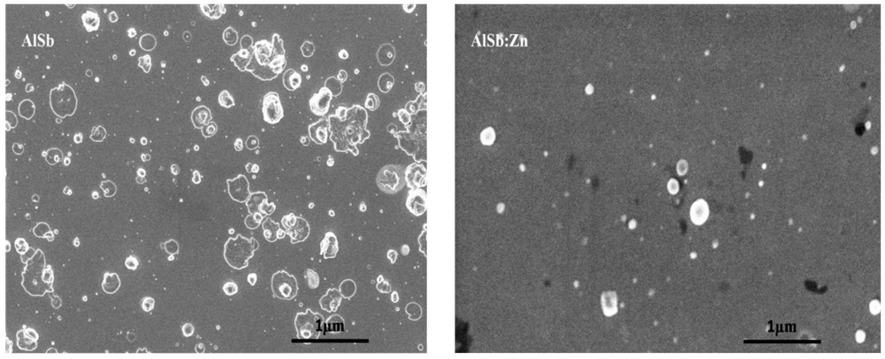
To compare the deliquescence of the AlSb and AlSb:Zn thin films, the films were stored in a vacuum chamber (about 2 Pa).
Figure 8 shows the SEM images of the AlSb and AlSb:Zn thin films stored in the vacuum chamber for 48 h. There were some agglomerates on the surface of the films after deliquescence. In the same vacuum chamber, the quantities of agglomerate of AlSb:Zn were fewer than AlSb. It indicated that Zn doping can reduce the deliquescent speed of AlSb thin films.
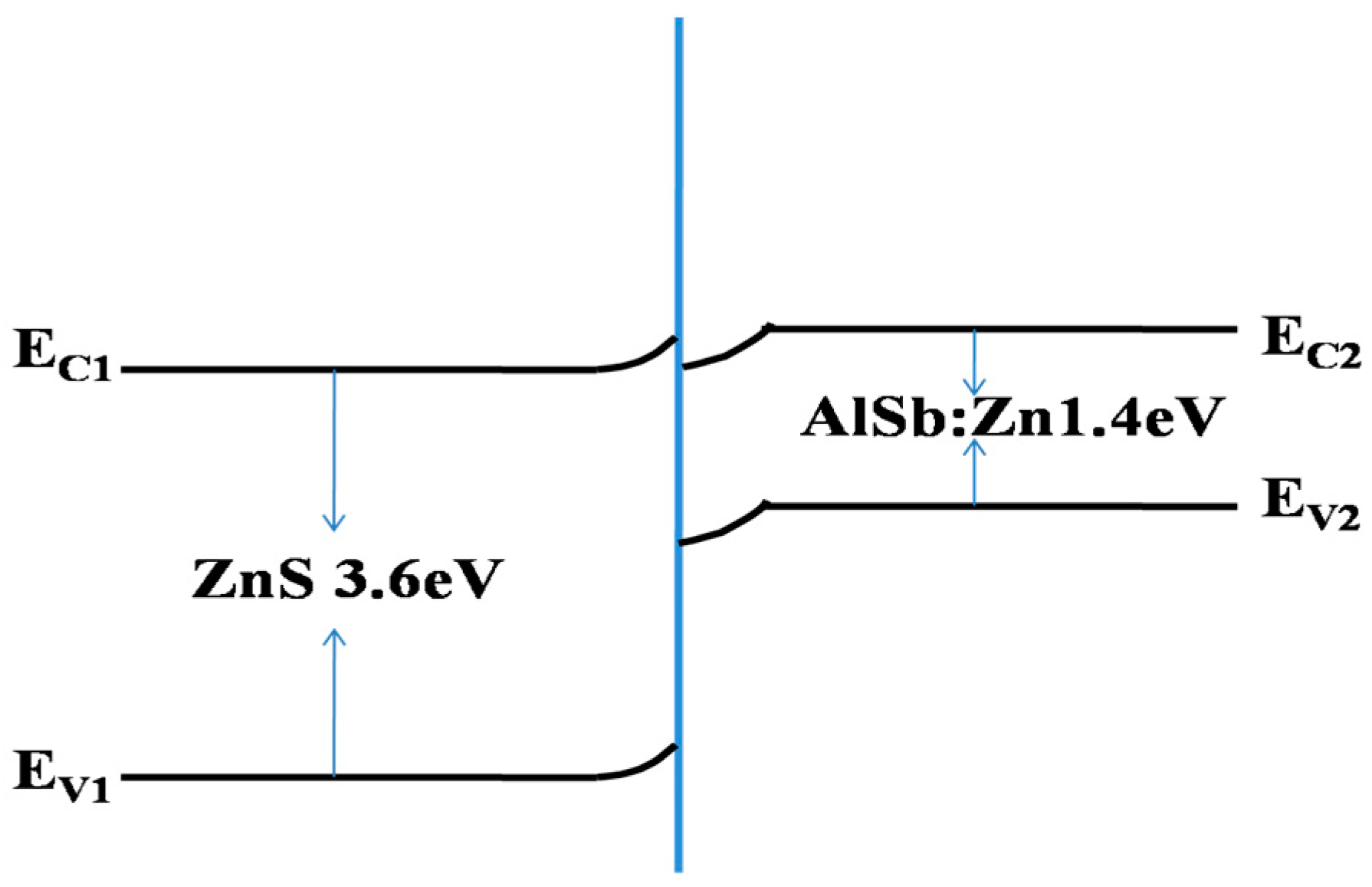
The purpose of studying AlSb-base solar cells is to get low cost and environmental solar cells. In our previous work, ZnS/AlSb thin film solar cells were simulated by using wxAMPS and high conversion efficiency was obtained in the solar cells [
15]. For the AlSb-base solar cells, ZnS is considered as one of the promising N-type buffer layer materials due to wide band gap and high transmittance [
22,
23]. Moreover, both of Zn and S elemental resources are abundant, low cost and environment-friendly. The PN junction is formed when ZnS films (N-type materials) are combined with AlSb:Zn films (P-type materials), as shown in
Figure 9. The build-in electrical field exists at the interface of ZnS and AlSb:Zn films, which is able to drive electrons away from the interface and accelerates the collection of electrons.
After the above studies, we fabricated AlSb-based solar cell with a structure of FTO/ZnS/AlSb:Zn/Au. AlSb:Zn thin film was deposited at the optimized condition. Over 60 mV light open circuit voltage was obtained in the AlSb:Zn-based solar cell. However, it was very difficult to obtain the light J-V curve because the short circuit current of the device was too small. The open circuit voltage was influenced by recombination of grain boundary, characteristics of interfaces, and carrier transportation.
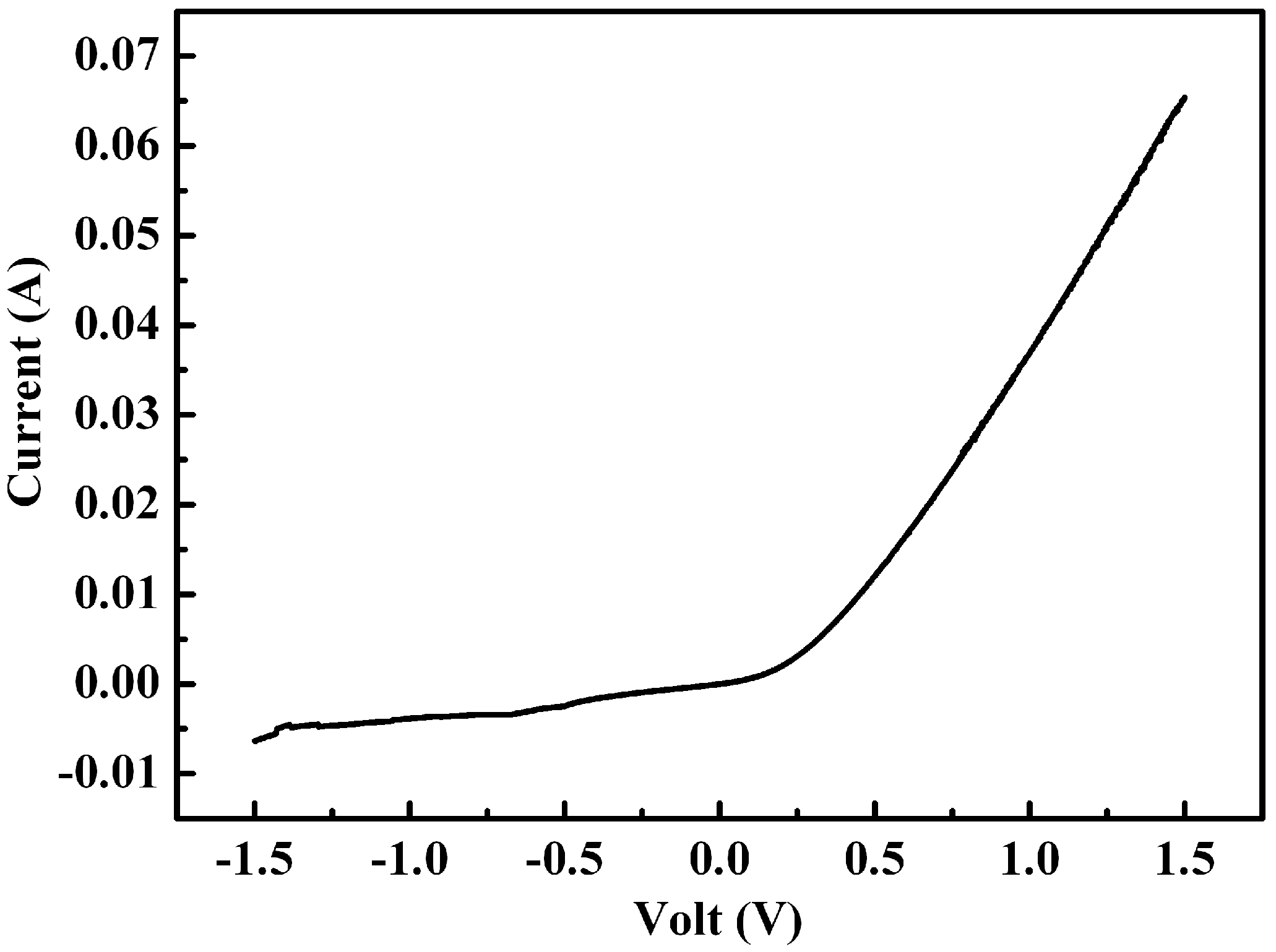
The dark
I-
V curve is shown in
Figure 10. The dark
I-
V curve shows the PN junction of ZnS/AlSb:Zn structure was combined. Environmental and low-cost AlSb-based PN junction diodes can be prepared by the economic PLD method. AlSb:Zn thin films are promising materials for photovoltaic and other optoelectronic devices. The values of the diode factor (
A) and the reverse saturation current density (
J0) calculated from dark
I-
V curve were 11.6 and 15.8 mA/cm
2, respectively. The high value of
A indicates that the defect density of the PN junction was very large and the recombination velocity of defect was high in the device [
24]. The high
J0 and leakage current have an effect on the open circuit voltage of the solar cells, so the open circuit voltage is very small. Our future work should mainly focus on optimizing the structure of the AlSb-based solar cell.


