Article

Fabrication of Cu2ZnSnS4 Thin Films Based on Facile Nanocrystals-Printing Approach with Rapid Thermal Annealing (RTA) Process

1
College of Sciences, Shanghai Institute of Technology, 100 Haiquan Road, Shanghai 201418, China
2
School of Science, East China University of Science and Technology, 130 Meilong Road, Shanghai 200237, China
3
Department of Applied Physics, Graduate School of Engineering, Osaka University, Yamadaoka, Suita-city, Osaka 565-0871, Japan
*
Authors to whom correspondence should be addressed.
Coatings 2019, 9(2), 130; https://doi.org/10.3390/coatings9020130
Submission received: 15 December 2018 / Revised: 1 February 2019 / Accepted: 13 February 2019 / Published: 19 February 2019

Abstract

:
In the current study, Cu2ZnSnS4 (CZTS) thin film was successfully fabricated by the facile nanocrystals (NCs)-printing approach combined with rapid thermal annealing (RTA) process. Firstly, the CZTS NCs were synthesized by a thermal solution method and the possible formation mechanism was analyzed briefly. Then the influences of RTA toleration temperature and duration time on the various properties of as-printed thin films were examined via XRD, Raman, FE-SEM, UV-vis-IR spectroscopy, EDS and XPS treatments in detail. As observed, the RTA factors of temperature and time had significant impacts on the structure and morphology of as-prepared thin films, while there were no obvious effects on the band gap energy in studied conditions. The results showed that the obtained thin film at optimal RTA conditions of (600 °C, 20 min) featured a kesterite structure in pure phase and an irregular morphology consisting of large grains. Moreover, the satisfactory composition of a Cu-poor, Zn-rich state and an ideal band gap energy of 1.4 eV suggests that as-fabricated CZTS thin film is a suitable light-absorbing layer candidate for the application in thin film solar cells.

Graphical Abstract

1. Introduction

In the last decade, copper-based quaternary semiconductor material Cu2ZnSnS4 (CZTS) has been widely considered as a most promising absorber layer candidate for low-cost thin film solar cells, owing to its high absorption coefficient (>104 cm−1) and optimal band gap (1.0–1.5 eV) that are ideal properties for the application under solar irradiation [1,2,3]. Furthermore, all the constituent elements of CZTS are naturally abundant and cheap, whereas the rare and expensive elements of In and Ga are employed in the well-known material of CuInxGa1−x(S,Se)2 (CIGS) [4,5,6]. The above are beneficial to realize the low-cost and high-volume production of solar cells. Additionally, according to Shockley–Queisser photon balance calculation, CZTS-based solar cells can achieve a theoretical conversion efficiency of ~32.2% [7,8]. To date, the efficiency of CZTS-based solar cells is around 12.6% reported by Mitzi group [9,10], demonstrating that CZTS features great potential as an absorption material applied in photovoltaic devices.
In early studies, the prevailing technologies for CZTS fabrication were mostly based on vacuum condition, such as sputtering [11,12], thermal evaporation [13,14], and pulsed laser deposition [15,16]. However, above-vacuum approaches were strictly limited by their intrinsic shortages of high-cost, complicated process and difficulty in scaling up production. Since 2010, the non-vacuum technique has been studied extensively, which was spurred by the excellent work of Todorov and his coworkers [17]. The reported conversion efficiency of CZTS-based solar cells, which was fabricated by a non-vacuum hydrazine solution route, was 9.66%. To date, diverse non-vacuum approaches have been developed for CZTS material fabrication, e.g., electrochemical deposition [18,19], sol–gel method [20,21], spray pyrolysis [22,23] and nanocrystals (NCs) ink coating route [24,25]. It is worth mentioning that Guo et al. reported an efficiency of 7.2% of CZTS-based solar cells via NCs ink coating route [26].
For the purpose of large-scale commercial production, the NCs-printing approach has been investigated widely for CZTS thin film fabrication over various non-vacuum deposition methods, owing to its excellent properties, e.g., simple operation requirement, high material utilization efficiency and good roll-to-roll compatibility. As noted, the deposition step is always followed by an annealing or sulfurization process, aiming to improve the various physical and chemical properties of as-obtained thin film. Rapid thermal annealing (RTA) technology, which could realize the rapid temperature rising or falling, presents more potential in the time-cost shortening comparing with traditional heat treatments. It has been applied in CIS/CIGS (CIS is the abbreviation of CuIn(S,Se)2) fabrication and exhibits excellent features for the promotion of sample properties, such as structure, morphology, etc. [27,28]. However, the systematic investigation on RTA application in the preparation of CZTS thin film is relatively less intensive.
In the current study, we firstly synthesized CZTS NCs by a thermal solution route, then the CZTS thin film was prepared via facile NCs-printing approach combined with RTA treatment. The influences of RTA factors (including toleration temperature and duration time) on the structural, compositional, morphological and optical properties of as-prepared CZTS thin films were investigated in detail. The proposed work aims to provide a rapid and facile fabrication process for CZTS thin film that is propitious to industrial production.

2. Experimental Details

2.1. Synthesis of CZTS NCs by Thermal Solution Route

In a typical synthesis, 1.5 mmol CuCl2·2H2O, 0.75 mmol Zn(CH3COO)2·2H2O, 0.75 mmol SnCl2 and 4.5 mmol thiourea were successively dissolved in 30 mL oleylamine with magnetic stirring at room temperature. The three-neck flask was employed as the vessel in current work. Then the mixed solution was heated to 250 °C and maintained for 1 h to let CZTS NCs grow. It was noted that the whole reaction process was undertaken in the anaerobic and anhydrous environment provided by air degassing and N2 purging. When the reaction finished, the solution was cooled to room temperature naturally. As-obtained products were centrifuged and washed with ethanol several times. Finally, the precipitates were dried by a thermal blower at 60 °C for several hours.

2.2. Deposition of CZTS Thin Film by NCs-Printing Approach

In the current study, the proposed NCs-printing approach was two steps: (1) printable paste preparation; (2) precursor film deposition. In the first step, 0.5 g CZTS NCs (grinded with 1 mL ethanol for 10 min), 0.25 g ethyl-cellulose and 1.67 g α-terpilenol were added into solvent ethanol to form a mixed solution, which was processed alternately via magnetic stirring (5 min) and ultrasonic oscillation (5 min) twice for homogeneous dispersal. Ethyl-cellulose and α-terpilenol were employed as dispersant and binder. Then the printable paste was obtained after the solvent evaporation performed by a rotary evaporator. In the second step, the paste was coated on the glass substrate via printing route. Sequentially, the printed film was dried at 250 °C for 1 min on a hot plate to obtain the precursor film. Then, the as-deposited thin film was processed via self-built RTA system under S + N2 atmosphere for the purpose of property improvement.

2.3. Characterization Methods for CZTS Material

The crystal structure was characterized by X-ray diffraction (XRD, MiniFlex 600, Rigaku, Tokyo, Japan) and Raman spectroscopy (i-Raman, B&W Tek, Newark, NJ, USA). The morphology was examined by field emission scanning electron microscopy (FE-SEM, QUANTA FEG450, FEI, Hillsboro, OR, USA). The optical property was measured with an UV-vis-IR double beam spectrophotometer (Lambda 1050, Perkin-Elmer, Waltham, MA, USA). The chemical composition was determined by energy dispersive X-ray spectroscopy (EDS, Genesis Apollo X, EDAX, Mahwah, NJ, USA). The valence state of constituent elements was confirmed via X-ray photoelectron spectroscopy (XPS, Axis Ultra DLD, Kratos, Manchester, UK).

3. Results and Discussion

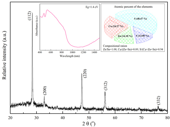
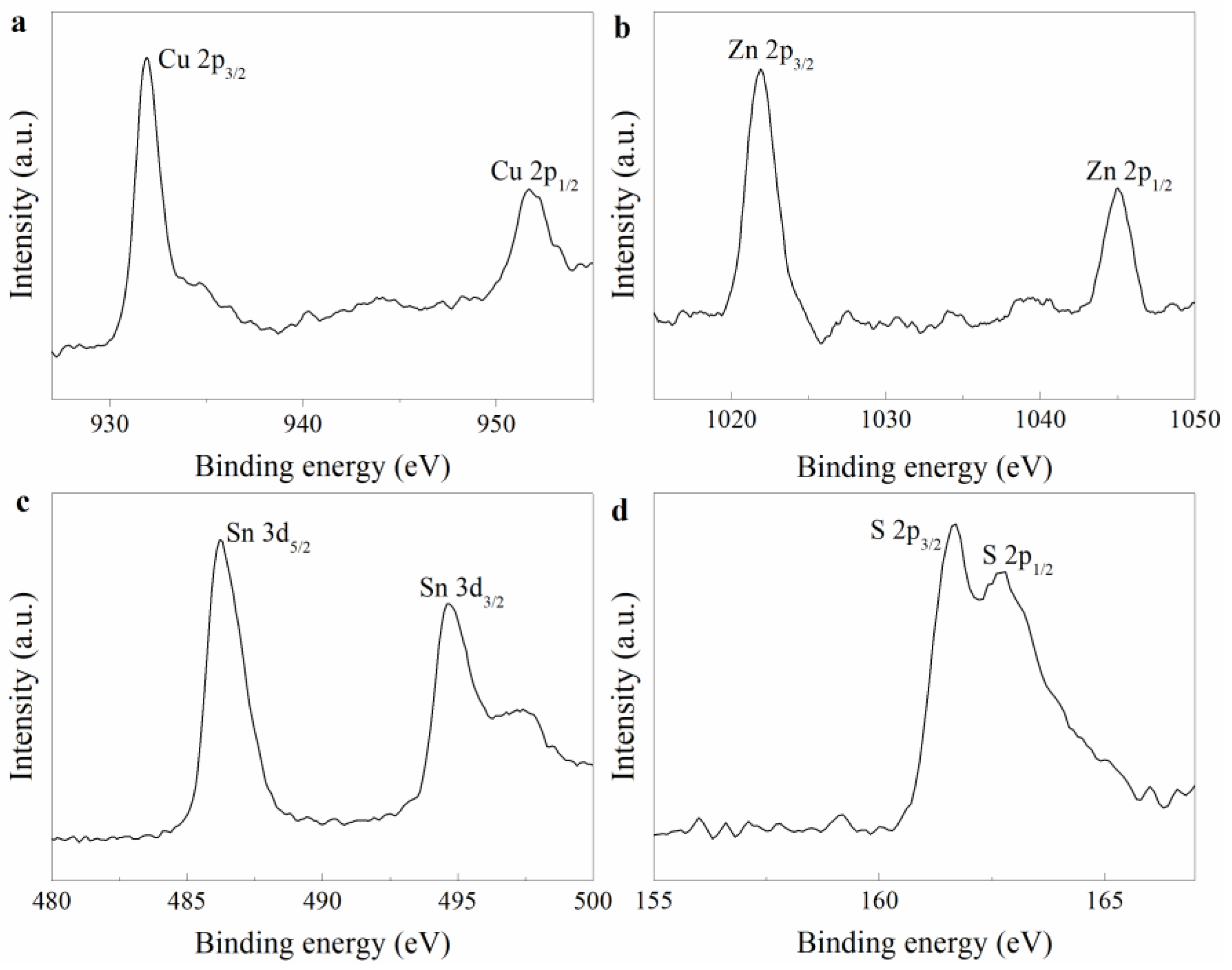
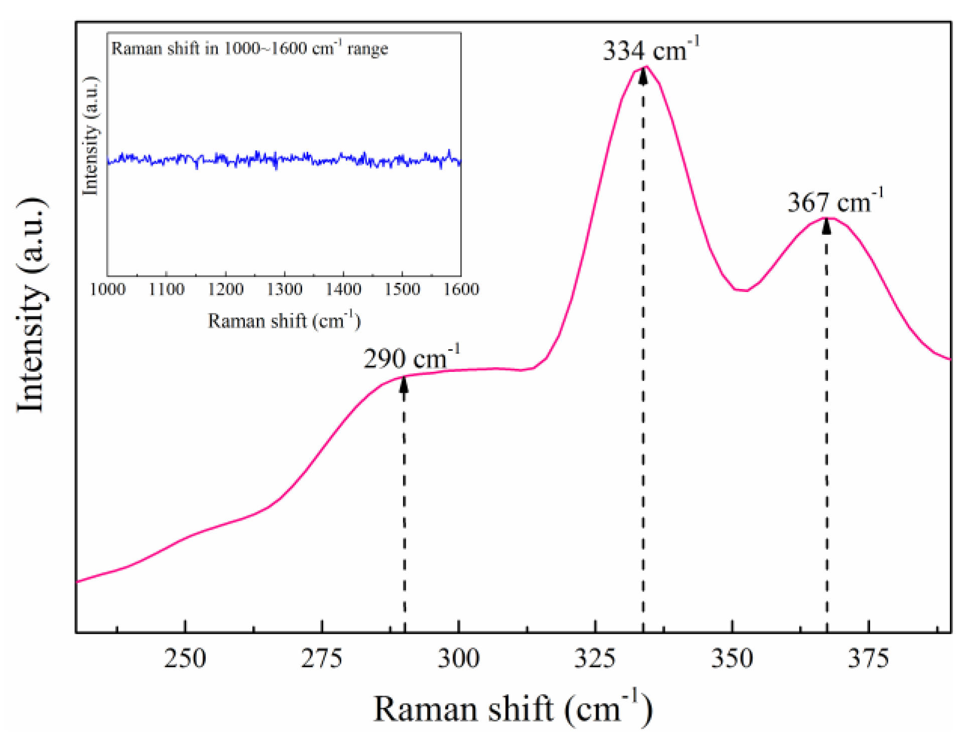
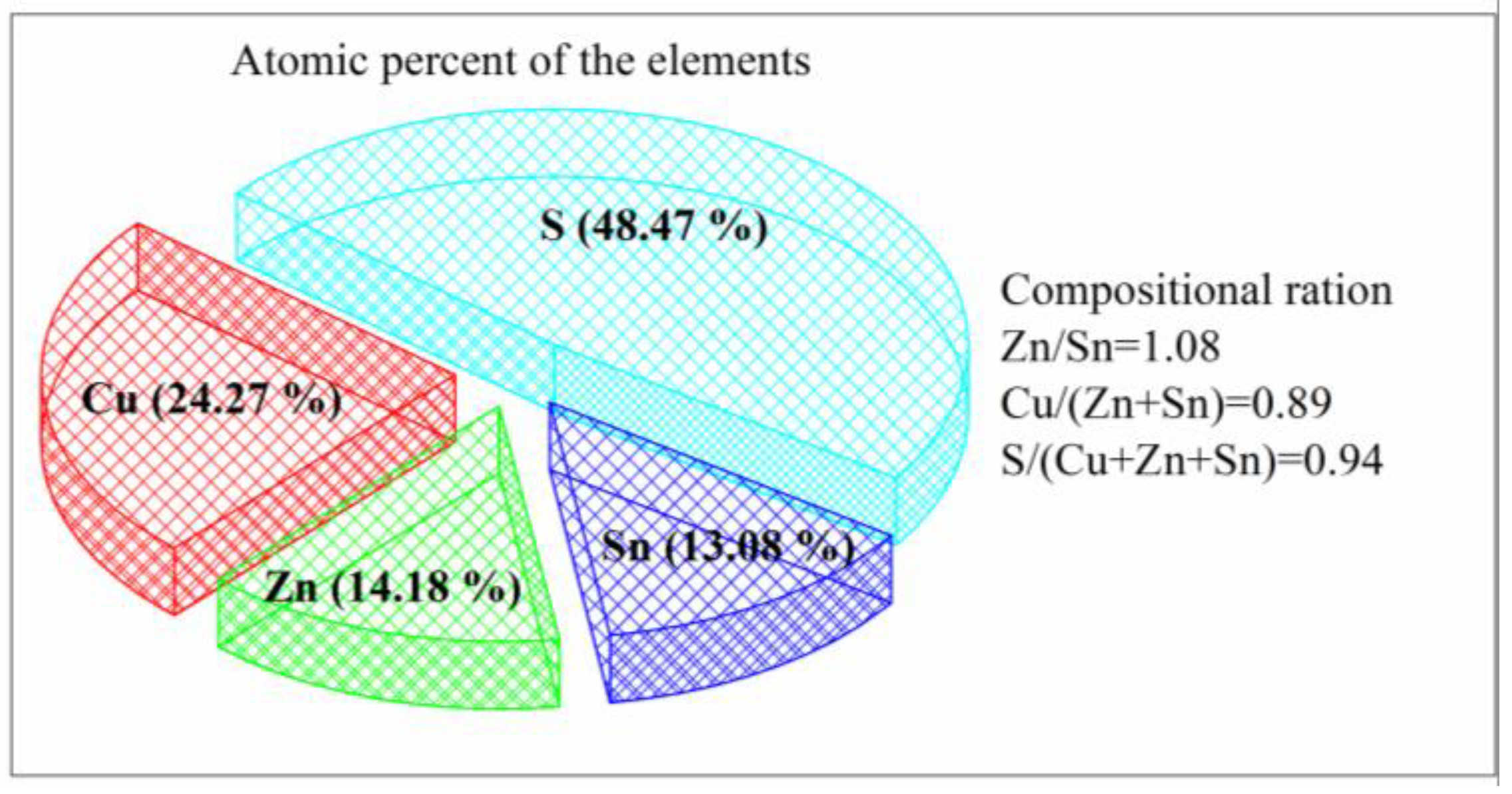
3.1. The Analysis of CZTS NCs Synthesis

In the present work, the thermal solution method was employed for the CZTS NCs synthesis. The possible synthesis mechanism was as follows. Firstly, the metal ions Cu2+, Sn2+ were dispersed homogeneously in the solution with the magnetic stirring, then the valence states of them were varied to be Cu+, Sn4+ derived from the oxidation and reduction process. In the second stage, Cu+, Zn2+, Sn4+ ions would coordinate with thiourea (Tu) to form Cu–Tu, Zn–Tu and Sn–Tu complexes. As the reaction proceeded, the complexes were decomposed and formed to be binary sulfides of Cu, Zn and Sn. Finally, the copper sulfides served as the initial nucleus to react with Zn and Sn sulfides, forming the CZTS NCs. The XRD pattern of the as-synthesized sample is shown in Figure 1a. As observed, the peaks appeared at around 2θ–28.5°, 33.0°, 47.5°, 56.0° and 76.5°, which could be attributed to the diffraction of the (112), (200), (220), (312) and (332) planes of kesterite CZTS (JCPDS 26-0575), respectively, as suggested by previous studies [29,30]. The kesterite CZTS is a typical tetragonal structure whereby each cation is bonded to four sulfur anions and each sulfur anion is bonded to four cations. The cation layers and anion layers are alternately arranged as CuZn/SS/CuSn/SS along the c-axis [31,32]. What’s more, above indicated that CZTS NCs could be grown successfully via present solution process. Unfortunately, some weak impurity (also could be called as secondary phase) peaks at around 26.8° and 30.2°, which could be attributed to the binary sulfide phases of Cu and Sn, were additionally observed. The presence of secondary phases was most likely related to the non-vacuum solution condition, the metal elements of Cu, Zn and Sn featured different reactivities in the used solvent, leading to an insufficient reaction.

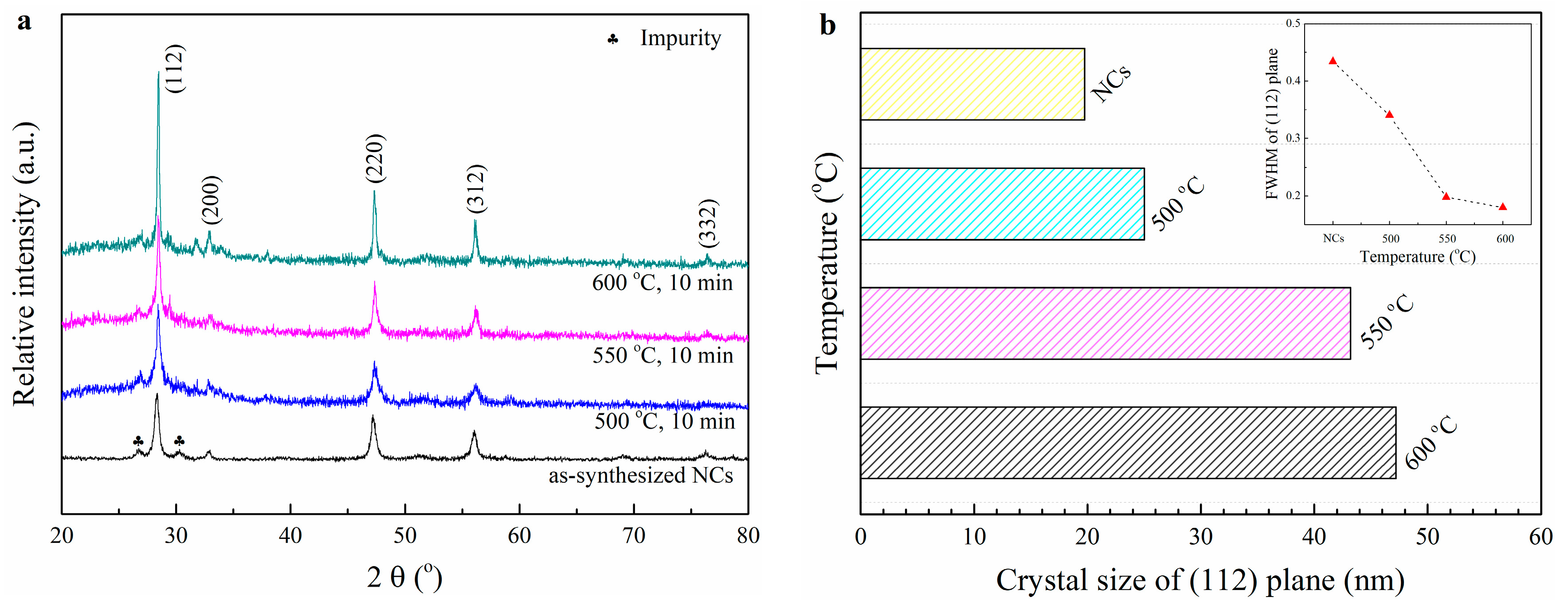
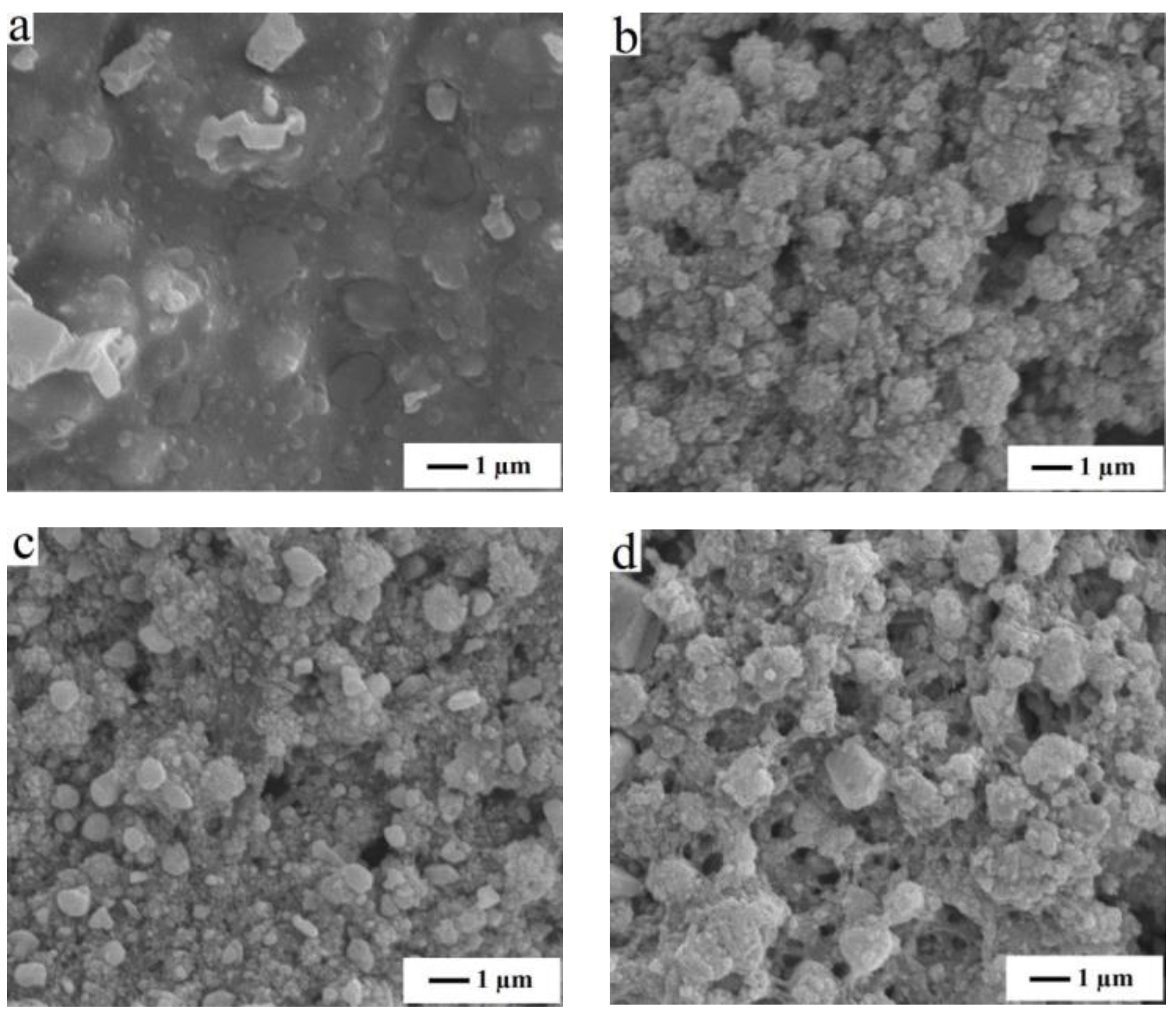
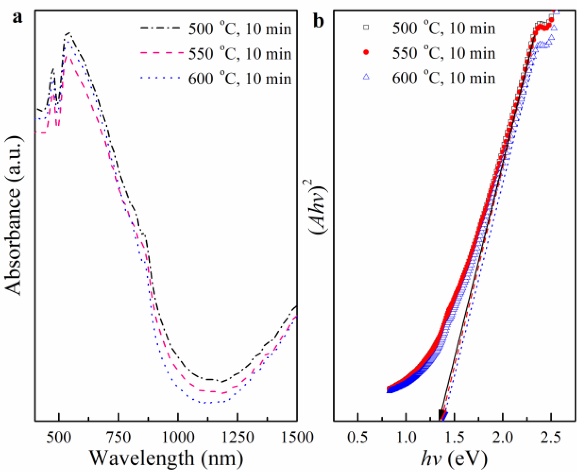
3.2. The Effects of RTA Toleration Temperature

To observe the influences of RTA toleration temperature on as-deposited CZTS thin films, the temperature value was varied from 500 to 600 °C in 50 °C increment while the duration time was set as a constant of 10 min. The XRD patterns of as-fabricated CZTS thin films are displayed in Figure 1a. As depicted, the peaks at around 2θ–28.5°, 33.0°, 47.5°, 56.0° and 76.5° corresponded to the (112), (200), (220), (312) and (332) planes of kesterite CZTS with tetragonal phase (JCPDS 26-0575), respectively, whereas the impurity peaks still existed in the whole temperature range. As noted, in the range of 500–600 °C, the peaks became sharper with annealing temperature increased, which meant the crystallinity improved gradually, especially in the (112) plane. Figure 1b shows the variations in the crystallite size of as-fabricated CZTS thin films, calculated from the (112) plane via Debye–Scherrer’s formula: D = kλ/βcosθ, as a function of RTA temperature. In this equation, D is the crystallite size, k is the Scherrer constant, λ is the wavelength of Cu Kα (0.15406 nm), β is the full width at half maximum (FWHM) of (112) peak and θ is the Bragg angle. It is worth mentioning that FWHM values showed a decreasing tendency observed in the inset of Figure 1b, which agreed well with the changes of diffraction peak shapes. Conversely, the crystallite size presented an increasing trend when RTA temperature raised, which stemmed from the relationship between D and β in above formula. Correspondingly, the crystallite sizes of CZTS NCs and thin films at various temperatures of 500, 550, 600 °C were 19.7, 25.0, 43.2, 47.2 nm, respectively.
The morphology images of CZTS thin films prepared by various RTA temperatures are shown in Figure 2. It was found that the unannealed thin film featured a mixture state with nanoparticles (NPs) and organics (ethyl-cellulose and α-terpilenol) (as shown in Figure 2a). This was mainly due to the previous drying process was unable to evaporate the organics used for printing effectively; the preferable temperature for these organics’ evaporation may be over 300 °C [27]. It was noted that the NPs were formed by the NCs aggregating during the synthesis process in solution, due to the high surface energy and Van der Waals forces [33]. As presented in Figure 2b–d, the organics could be thermal decomposed and evaporated gradually with RTA temperature increased in the range of 500–600 °C. However, it was observed that some voids appeared on the surface of as-prepared thin films with the above evaporation process. Although the surface of obtained thin films prepared under various RTA temperatures presented as an uncompact and non-uniform state, it may be beneficial for the evaporation of organics and reducing the residue of the amorphous carbon layer in the bottom of the thin films [28]. Additionally, the NPs size on the thin film surface variated in an upward tendency due to the coalescence and recrystallization process. It is also worth mentioning that the large grain is beneficial to boost the photoelectric performance of a photovoltaic device, due to the large grain in the absorber layer could maximize the minority carrier diffusion length and reduce the recombination rate of photo-generated carriers [34,35].
The optical properties of as-fabricated thin films with different RTA temperatures were determined by UV-vis-IR spectroscopy in transmission mode, and the results are displayed in Figure 3. The valence band of CZTS consists of an anti-bonding linear combination of Cu 3d and S 3p states, and the conduction band is dominated by an isolated band made up by Sn 5s and S 3p states. In the visible region, the optical property of CZTS is decided by the transitions from Cu 3d/S 3p states to the conduction band [36]. As observed in Figure 3a, the absorption edge of CZTS thin films became steeper with the increasing of RTA temperature in the 500–600 °C range. This indicated that the crystallinity of as-fabricated thin films improved gradually as the temperature raised, well consistent with the XRD analysis. In the present study, the band gap energy Eg of CZTS thin films fabricated under various temperatures was determined by extrapolating the straight line of the plot (Ahv)2 versus (hv) (A = absorbance, h = Planck’s constant and v = frequency). As observed in Figure 3b, the Eg values of as-prepared samples were variated slightly around 1.4 eV in the whole range of 500–600 °C regardless of the temperature changing. The above Eg value was comparable to the optimum value of 1.4–1.5 eV for the photovoltaic conversion in single-band-gap devices.
Based on above analyses, the properties of structure, morphology and optical property of as-obtained thin film fabricated with the RTA conditions of (600 °C, 10 min) featured better than others, which indicated that the toleration temperature of 600 °C was preferable for the next study.

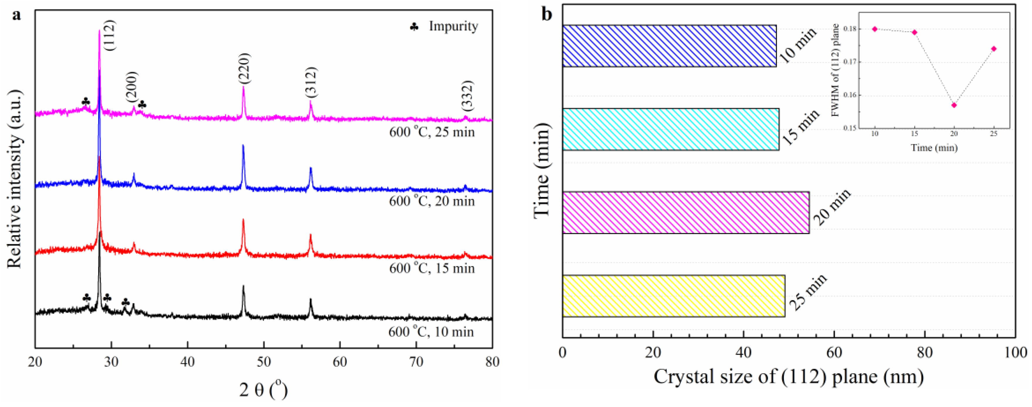
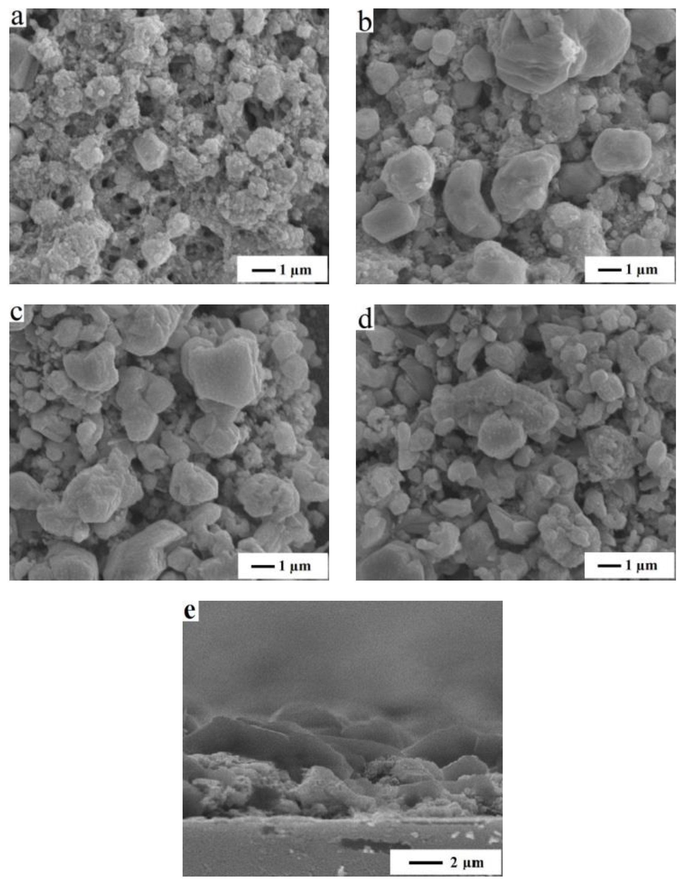
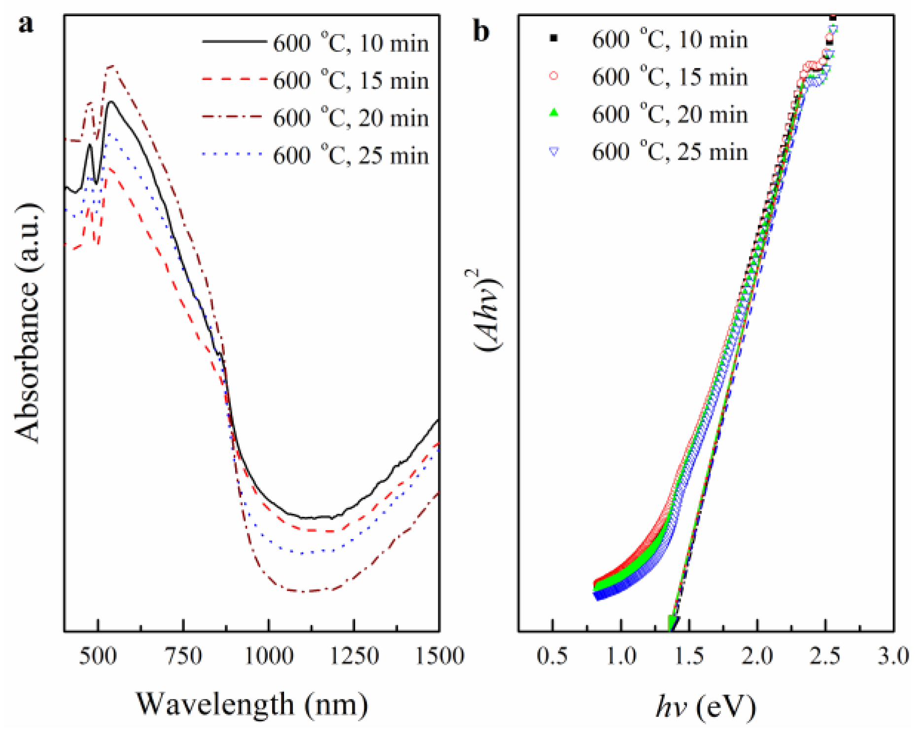
3.3. The Effects of RTA Duration Time

The effects of RTA duration time on the CZTS thin films, with a fixed temperature of 600 °C, were studied in detail by setting the time in the range of 10–25 min with an increment of 5 min. Figure 4a gives the XRD patterns of CZTS thin films fabricated with different RTA duration time. As observed, the diffraction peaks of the (112), (200), (220), (312) and (332) planes appeared at around 2θ–28.5°, 33.0°, 47.5°, 56.0° and 76.5°, respectively, which suggested the existence of tetragonal kesterite CZTS product. In the range of 10–20 min, it was found that the intensity of diffraction peaks raised and the shape became sharper, indicating the crystallinity improved with RTA time prolonged. It was noted that the impurities also disappeared with duration time increased to 15–20 min, illustrating the atoms of each elements (Cu, Zn, Sn and S) in as-fabricated samples were arranged more orderly, then the CZTS product featured as a pure phase of kesterite structure. However, the impurity peaks reappeared and the diffraction intensity declined when the duration time was prolonged to 25 min. This may be owed to the decomposition of the CZTS product in a longer reaction time.
As depicted in Figure 4b, the FWHM values of the (112) plane showed a decreasing trend in the range of 10–20 min, then became larger suddenly when the duration time was over 20 min. This tendency agreed well with the variations of XRD patterns. Correspondingly, the crystallite sizes of CZTS thin films, with RTA time of 10, 15, 20 and 25 min, were 47.2, 47.8, 54.5 and 49.1 nm, respectively, and featured a reverse trend compared with FWHM values.
However, due to cubic ZnS and tetragonal Cu2SnS3 have similar diffraction patterns with kesterite CZTS, it is difficult to distinguish CZTS and above compounds clearly just by XRD treatment. Raman is a useful complimentary technique to identify above impurity phases based on the fact that CZTS, Cu2SnS3 and ZnS have different vibration features. Herein, we chose the as-obtained sample fabricated under the duration time of 20 min, which featured the best crystallinity, for the further Raman analysis via the near-resonant excitation of 785 nm. It is worth mentioning that the used wavelength could enhance the detected peak intensity, and has an outstanding penetration depth of ~400 nm compared with other wavelengths as suggested by early studies [37]. As shown in Figure 5, the Raman shifts of as-fabricated CZTS thin film, located at 290, 334 and 367 cm−1 could be assigned to kesterite CZTS reported by previous work [38]. It is worth mentioning that there were no characteristic Raman peaks of Cu2SnS3 at 303, 318 cm−1 and ZnS at 275, 352 cm−1 [39,40], which demonstrated the absences of ZnS and Cu2SnS3. This suggested the as-prepared sample was pure CZTS with kesterite structure. Additionally, the Raman spectra in the 1000–1600 cm−1 range is also displayed as an inset in Figure 5. As depicted, there was no typical Raman peak of carbon at around 1360 or 1580 cm−1, which indicated the absence of carbon residue originating from the organics of the printable paste.
Figure 6 shows the morphology images of as-obtained CZTS thin films with various RTA duration time. As observed, with the RTA time prolonged, the residual organics in the thin film could be evaporated effectively, which was well demonstrated by Raman analysis. In the whole time range of 10–25 min, the recrystallization process became more and more significant with the reaction time extended. In the range of 10–15 min, the recrystallization mainly occurred on the surface of as-deposited thin films, as shown in Figure 6a,b. While the time was over 15 min (20–25 min), the regrowth process also took place in the bottom, as described in Figure 6c–e. Meanwhile, the NPs size and shape of the fabricated thin films became larger and clean-cut, respectively, and the samples presented an irregular morphology consisting of NPs in the whole duration time range. In addition, the existence of voids also was improved to a certain degree with the above process, but still needs further improvement in next study.
The optical properties of as-obtained CZTS thin films are given in Figure 7. As depicted in Figure 7a, the absorption edge of as-prepared samples became steeper with RTA duration time extended in 10–20 min range, suggesting the crystallinity of CZTS thin films improved. While the reaction time was 25 min, the steep degree fell down which meant the crystallinity decreased. Additionally, the above also kept in good accordance with the analysis of XRD patterns. Additionally, the band gap energies of as-obtained thin films, fabricated with different reaction time, fluctuated around 1.4 eV similar to the trend in Section 3.2.
All the above analyses suggest that when the duration time was 20 min, the structural, morphological and optical properties of as-prepared thin film were more advantageous for the application as an absorption layer in photovoltaic devices. Herein, the energy dispersive X-ray spectroscopy (EDS) was employed for the further composition observation of the obtained sample, and the result is shown in Figure 8. It revealed that the atom ratios of Cu, Zn, Sn, S were 24.27:14.18:13.08:48.47 = 1.86:1.08:1:3.71, close to theoretical stoichiometric value of 2:1:1:4. The ratios of Zn/Sn, Cu/(Zn + Sn) and S/(Cu + Zn + Sn) were 1.08, 0.89 and 0.94, respectively. The results indicated the as-obtained CZTS thin film featured a Cu-poor and Zn-rich state, which may be beneficial for photovoltaic performance as suggested by earlier work [41]. This is due to the Cu-poor state enhances the formation of Cu vacancies to increase shallow acceptors in CZTS, while the Zn-rich state suppresses the substitution of Cu at Zn sites for the raising of relatively deep acceptors [42].
Furthermore, X-ray photoelectron spectroscopy (XPS) was used to confirm the constitution of above CZTS thin film. The valence states of all four elements: Cu 2p, Zn 2p, Sn 3d and S 2p in CZTS thin film is displayed in Figure 9. As observed in Figure 9a, the binding energy peaks for Cu 2p3/2 and Cu 2p1/2 are located at 931.9 and 951.7 eV, respectively, with a peak splitting of 19.8 eV, indicating the formation of Cu (I). In the Zn 2p XPS spectrum (Figure 9b), two peaks appeared at 1021.9 and 1045 eV, with a separation of 23.1 eV, which could be assigned respectively to Zn 2p3/2 and Zn 2p1/2 suggesting the existence of Zn (II). As shown in Figure 9c, the peaks of Sn 3d5/2 and Sn 3d3/2 were observed at 486.2 and 494.6 eV, with a peak splitting of 8.4 eV, confirming the configuration of Sn (IV). The S 2p core-level spectrum in Figure 9d gives two peaks located at 161.7 and 162.7 eV, which coincided with the 160–164 eV range of S in the sulfide phases [43].

4. Conclusions

In summary, the CZTS thin film was successfully fabricated via the facile NCs-printing route combined with the RTA process. The effects of the RTA conditions (temperature and time) on the various properties of as-obtained thin film were confirmed via XRD, Raman, FE-SEM, UV-vis-IR spectroscopy, EDS and XPS treatments in detail. As investigated, the structure and morphology of as-fabricated CZTS thin film positively correlated with the variations of RTA temperature in the 500–600 °C range and duration time in the 10–20 min range. Interestingly, it could be found that the band gap energy of as-obtained CZTS thin film was almost invariable regardless of the changes of RTA conditions in the present work. The results indicated that the RTA conditions of (600 °C, 20 min), compared with others investigated in the current work, may be more advantageous for obtaining the high-performance CZTS thin film. The as-prepared thin film presented a pure phase of kesterite structure, and an irregular morphology with large grains. Meanwhile, the features of Cu-poor, Zn-rich state of chemical composition and direct band gap energy of 1.4 eV were optimal for photovoltaic application. Further work is to fabricate a high-performance optoelectronic device with as-obtained CZTS thin film.

Author Contributions

Conceptualization, J.C. and F.W.; Methodology, J.C., F.W. and Q.C.; Formal analysis, J.C and Q.C.; Investigation, J.C., B.Y. and X.P.; writing—original draft preparation, J.C.; writing—review and editing, J.Z. and X.D.; Supervision, F.W.; Project administration, J.C.; Funding acquisition, J.C.

Funding

The project was sponsored by Shanghai Sailing Program, China (No. 18YF1422500), Research start-up project of Shanghai Institute of Technology (No. YJ2018-9), Science and Technology Planning Project of Zhejiang Province, China (No. 2018C01046), and Enterprise-funded Latitudinal Research Projects (Nos. J2016-141, J2017-171, J2017-293 and J2017-243).

Conflicts of Interest

The authors declare no conflict of interest.

References

  1. Shi, L.; Pei, C.; Xu, Y.; Li, Q. Template-directed synthesis of ordered single-crystalline nanowires arrays of Cu2ZnSnS4 and Cu2ZnSnSe4. J. Am. Chem. Soc. 2011, 133, 10328–10331. [Google Scholar] [CrossRef] [PubMed]
  2. Chen, J.; Chen, Q.; Ni, Y.; Wang, T. Facile fabrication of Cu2ZnSnS4 thin film based on a novel metal-salt precursor printing route. Mater. Lett. 2015, 143, 185–187. [Google Scholar] [CrossRef]
  3. Cui, H.; Liu, X.; Sun, L.; Liu, F. Fabrication of efficient Cu2ZnSnS4 solar cells by sputtering single stoichiometric target. Coatings 2017, 7, 19. [Google Scholar] [CrossRef]
  4. Kaur, K.; Kumar, N.; Kumar, M. Strategic review of interface carrier recombination in earth abundant Cu-Zn-Sn-S-Se solar cells: Current challenges and future prospects. J. Mater. Chem. A 2017, 5, 3069–3090. [Google Scholar] [CrossRef]
  5. Shin, D.; Saparov, B.; Mitzi, D.B. Photovoltaic materials: Defect engineering in multinary earth bundant chalcogenide photovoltaic materials. Adv. Energy Mater. 2017, 7, 1602366. [Google Scholar] [CrossRef]
  6. Chen, J.; Chen, Q.; Wang, T.; Zhou, F. The synthesis of Cu2ZnSnS4 nanocrystals prepared by a facile calcination route in the atmosphere. Mater. Lett. 2014, 125, 206–208. [Google Scholar] [CrossRef]
  7. Katagiri, H.; Jimbo, K.; Maw, W.S.; Oishi, K. Development of CZTS-based thin film solar cells. Thin Solid Films 2009, 517, 2455–2460. [Google Scholar] [CrossRef]
  8. Kahraman, S.; Çetinkaya, S.; Podlogar, M.; Bernik, S. Effects of the sulfurization temperature on sol gel-processed Cu2ZnSnS4 thin films. Ceram. Int. 2013, 39, 9285–9292. [Google Scholar] [CrossRef]
  9. Li, J.; Wang, D.; Li, X.; Zeng, Y. Cation substitution in earth-abundant kesterite photovoltaic materials. Adv. Sci. 2018, 5, 1700744. [Google Scholar] [CrossRef] [PubMed]
  10. Wang, W.; Winkler, M.T.; Gunawan, O.; Gokmen, T. Device characteristics of CZTSSe thin-film solar cells with 12.6% efficiency. Adv. Energy Mater. 2014, 4, 1301465. [Google Scholar] [CrossRef]
  11. Jimbo, K.; Kimura, R.; Kamimura, T.; Yamada, S. Cu2ZnSnS4-type thin film solar cells using abundant materials. Thin Solid Films 2007, 515, 5997–5999. [Google Scholar] [CrossRef]
  12. Liu, F.; Li, Y.; Zhang, K.; Wang, B. In situ growth of Cu2ZnSnS4 thin films by reactive magnetron co-sputtering. Sol. Energy Mater. Sol. C 2010, 94, 2431–2434. [Google Scholar] [CrossRef]
  13. Repins, I.; Beall, C.; Nirav, V.; DeHart, C. Co-evaporated Cu2ZnSnSe4 films and devices. Sol. Energy Mater. Sol. C 2012, 101, 154–159. [Google Scholar] [CrossRef]
  14. Schubert, B.A.; Marsen, B.; Cinque, S.; Unold, T. Cu2ZnSnS4 thin film solar cells by fast coevaporation. Prog. Photovolt. 2011, 19, 93–96. [Google Scholar] [CrossRef]
  15. Moriya, K.; Tanaka, K.; Uchiki, H. Fabrication of Cu2ZnSnS4 thin-film solar cell prepared by pulsed laser deposition. Jpn. J. Appl. Phys. 2007, 46, 5780–5781. [Google Scholar] [CrossRef]
  16. Sun, L.; He, J.; Kong, H.; Yue, F. Structure, composition and optical properties of Cu2ZnSnS4 thin films deposited by pulsed laser deposition method. Sol. Energy Mater. Sol. C 2011, 95, 2907–2913. [Google Scholar] [CrossRef]
  17. Todorov, T.K.; Reuter, K.B.; Mitzi, D.B. High-efficiency solar cell with earth-abundant liquid-processed absorber. Adv. Mater. 2010, 22, E156–E159. [Google Scholar] [CrossRef]
  18. Ahmed, S.; Reuter, K.B.; Gunawan, O.; Guo, L. A high efficiency electrodeposited Cu2ZnSnS4 solar cell. Adv. Energy Mater. 2012, 2, 253–259. [Google Scholar] [CrossRef]
  19. Ennaoui, A.; Lux-Steiner, M.; Weber, A.; Abou-Ras, D. Cu2ZnSnS4 thin film solar cells from electroplated precursors: Novel low-cost perspective. Thin Solid Films 2009, 517, 2511–2514. [Google Scholar] [CrossRef]
  20. Tanaka, K.; Fukui, Y.; Moritake, N.; Uchiki, H. Chemical composition dependence of morphological and optical properties of Cu2ZnSnS4 thin films deposited by sol-gel sulfurization and Cu2ZnSnS4 thin film solar cell efficiency. Sol. Energy Mater. Sol. C 2011, 95, 838–842. [Google Scholar] [CrossRef]
  21. Tanaka, K.; Oonuki, M.; Moritake, N.; Uchiki, H. Cu2ZnSnS4 thin film solar cells prepared by non-vacuum processing. Sol. Energy Mater. Sol. C 2012, 93, 583–587. [Google Scholar] [CrossRef]
  22. Vigil-Galán, O.; Espíndola-Rodríguez, M.; Courel, M.; Fontané, X. Secondary phases dependence on composition ratio in sprayed Cu2ZnSnS4 thin films and its impact on the high power conversion efficiency. Sol. Energy Mater. Sol. C 2013, 117, 246–250. [Google Scholar] [CrossRef]
  23. Kamoun, N.; Bouzouita, H.; Rezig, B. Fabrication and characterization of Cu2ZnSnS4 thin films deposited by spray pyrolysis technique. Thin Solid Films 2007, 515, 5949–5952. [Google Scholar] [CrossRef]
  24. Zhou, Z.; Wang, Y.; Xu, D.; Zhang, Y. Fabrication of Cu2ZnSnS4 screen printed layers for solar cells. Sol. Energy Mater. Sol. C 2010, 94, 2042–2045. [Google Scholar] [CrossRef]
  25. Chen, Q.M.; Dou, X.M.; Li, Z.Q.; Cheng, S.Y. Preparation of Cu2ZnSnS4 film by printing process for low-cost solar cell. Adv. Mater. Res. 2011, 335, 1406–1411. [Google Scholar] [CrossRef]
  26. Guo, Q.; Ford, G.M.; Yang, W.C.; Walker, B.C. Fabrication of 7.2% efficient CZTSSe solar cells using CZTS nanocrystals. J. Am. Chem. Soc. 2010, 132, 17384. [Google Scholar] [CrossRef] [PubMed]
  27. Kuo, H.P.; Tsai, H.A.; Huang, A.N.; Pan, W.C. CIGS absorber preparation by non-vacuum particle-based screen printing and RTA densification. Appl. Energy 2016, 164, 1003–1011. [Google Scholar] [CrossRef]
  28. Chen, Q.; Dou, X.; Li, Z.; Cheng, S. Printed ethyl cellulose/CuInSe2 composite light absorber layer and its photovoltaic effect. J. Phys. D Appl. Phys. 2011, 44, 455401–455406. [Google Scholar] [CrossRef]
  29. Todorov, T.; Kita, M.; Carda, J.; Escribano, P. Cu2ZnSnS4 films deposited by a soft-chemistry method. Thin Solid Films 2009, 517, 2541–2544. [Google Scholar] [CrossRef]
  30. Moholkar, A.V.; Shinde, S.S.; Agawane, G.L. Studies of compositional dependent CZTS thin film solar cells by pulsed laser deposition technique: An attempt to improve the efficiency. J. Alloy. Compd. 2012, 544, 145–151. [Google Scholar] [CrossRef]
  31. Chen, J.; Chen, Q.; Ni, Y.; Yamaguchi, Y. The synthesis of Cu2ZnSnS4 nanoparticles via an open-air solution route: Influences of Zn precursor content. J. Sol-Gel Sci. Technol. 2015, 75, 25–30. [Google Scholar] [CrossRef]
  32. Guo, Q.; Hillhouse, H.W.; Agrawal, R. Synthesis of Cu2ZnSnS4 nanocrystal ink and its use for solar cells. J. Am. Chem. Soc. 2009, 131, 11672–11673. [Google Scholar] [CrossRef] [PubMed]
  33. Wang, W.; Shen, H.; Jiang, F.; He, X. Low-cost chemical fabrication of Cu2ZnSnS4 microparticles and film. J. Mater. Sci. Mater. Electron. 2013, 24, 1813–1817. [Google Scholar] [CrossRef]
  34. Basha, S.S.; Rao, M.C. Effect of annealing temperature on structural and morphological studies of electrodeposited CZTS thin films. Ceram. Int. 2018, 44, 648–656. [Google Scholar] [CrossRef]
  35. Vanalakar, S.A.; Shin, S.W.; Agawane, G.L.; Suryawanshi, M.P. Effect of post-annealing atmosphere on the grain-size and surface morphological properties of pulsed laser deposited CZTS thin films. Ceram. Int. 2014, 40, 15097–15103. [Google Scholar] [CrossRef]
  36. Paier, J.; Asahi, R.; Nagoya, A.; Kresse, G. Cu2ZnSnS4 as a potential photovoltaic material: A hybrid Hartree-Fock density functional theory study. Phys. Rev. B 2009, 79, 115126. [Google Scholar] [CrossRef]
  37. Fernandes, P.A.; Salomé, P.M.P.; Cunha, A.F.D. Study of polycrystalline Cu2ZnSnS4 films by Raman scattering. J. Alloy. Compd. 2011, 509, 7600–7606. [Google Scholar] [CrossRef]
  38. Gao, C.; Shen, H.; Jiang, F.; Guan, H. Preparation of Cu2ZnSnS4 film by sulfurizing solution deposited precursors. Appl. Surf. Sci. 2012, 261, 189–192. [Google Scholar] [CrossRef]
  39. Wei, M.; Du, Q.; Wang, D.; Liu, W. Synthesis of spindle-like kesterite Cu2ZnSnS4 nanoparticles using thiorea as sulfur source. Mater. Lett. 2012, 79, 177–179. [Google Scholar] [CrossRef]
  40. Li, J.; Shen, J.; Li, Z.; Li, X. Wet chemical route to the synthesis of kesterite Cu2ZnSnS4 nanocrystals and their applications in lithium ion batteries. Mater. Lett. 2013, 92, 330–333. [Google Scholar] [CrossRef]
  41. Wangperawong, A.; King, J.S.; Herron, S.M. Aqueous bath process for deposition of Cu2ZnSnS4 photovoltaic absorbers. Thin Solid Films 2011, 519, 2488–2492. [Google Scholar] [CrossRef]
  42. Chen, S.; Gong, X.G.; Walsh, A.; Wei, S.H. Defect physics of the kesterite thin-film solar cell absorber Cu2ZnSnS4. Appl. Phys. Lett. 2010, 96, 021902. [Google Scholar] [CrossRef]
  43. Tang, D.; Wang, Q.; Liu, F.; Zhao, L. An alternative route towards low-cost Cu2ZnSnS4 thin film solar cells. Surf. Coat. Technol. 2013, 232, 53–59. [Google Scholar] [CrossRef]
Figure 1. (a) XRD patterns and (b) crystallite size and full width at half maximum (FWHM) of Cu2ZnSnS4 nanocrystals (CZTS NCs) and thin films.
Coatings 09 00130 g001
Figure 2. SEM images of CZTS thin films with different rapid thermal annealing (RTA) temperatures: (a) unannealed sample, (b) 500 °C, (c) 550 °C, (d) 600 °C.
Coatings 09 00130 g002
Figure 3. (a) Absorption spectra and (b) plots of (Ahv)2 vs. (hv) of CZTS thin films with different RTA temperatures.
Coatings 09 00130 g003
Figure 4. (a) XRD patterns and (b) crystallite size and FWHM of CZTS thin films with various RTA time.
Coatings 09 00130 g004
Figure 5. The Raman spectrum of CZTS thin film fabricated with the RTA conditions of (600 °C, 20 min).
Coatings 09 00130 g005
Figure 6. SEM images of CZTS thin films with different RTA time: (a) 10 min, (b) 15 min, (c) 20 min, (d) 25 min, (e) cross section image of 20 min.
Coatings 09 00130 g006
Figure 7. (a) Absorption spectra and (b) plots of (Ahv)2 vs. (hv) of CZTS thin films with various RTA time.
Coatings 09 00130 g007
Figure 8. The chemical composition of as-obtained CZTS thin film fabricated with RTA conditions of (600 °C, 20 min).
Coatings 09 00130 g008
Figure 9. The XPS spectrum of CZTS thin film fabricated with RTA conditions of (600 °C, 20 min).
Coatings 09 00130 g009

