Abstract
In this work, titanium nitride (TiN) nanorod arrays were fabricated using glancing angle deposition in a magnetron sputtering system. The deposition parameters, including the bias on the substrate and the flow rate of nitrogen, were varied to deposit various TiN nanorod arrays. Before glancing angle deposition was conducted, uniform TiN films were deposited and their permittivity spectra, for various deposition parameters, were obtained. The effect of the deposition parameters on the morphology of the nanorods is analyzed here. The polarization-dependent extinctance spectra of TiN nanorod arrays were measured and compared. Extinction, which corresponds to the longitudinal mode of localized surface plasmon resonance, can be significantly changed by tuning the N2 flow rate and substrate bias voltage during deposition.
1. Introduction
Noble metal nanoparticles with light-induced excitations, known as localized surface plasmon resonances (LSPRs) [1], have been widely exploited in optical nanoantennas [2], energy harvesting devices [3], ultrafast optical switching technologies [4,5], data storage [6], surface-enhanced Raman scattering [7], sensor applications [8], and biophotonics [9]. These resonances provide extremely large, highly localized electric field enhancements in the immediate vicinity of the metal nanoparticles. The frequency of LSPR is controlled by the size and shape of the metal nanoparticles [10]. For an assembly of silver nanorods, the dependence of resonant frequency on the aspect ratio of the rods is weaker than a single silver nanorod [11]. In most applications, the resonant frequency needs to match the frequency of incident light wave. It is an aim for scientists and engineers to be able to modulate the plasmonic resonant frequency of a nanostructure without changing the morphology.
Recently, transition metal nitrides (TMNs) have been developed as alternative plasmonic materials to novel metals [12]. TiN is mechanically and chemically stable [13]. The carrier concentration and mobility of TMNs are sufficiently high to generate negative real permittivity and low material loss. TMNs such as tungsten and tantalum nitrides have excellent refractory properties, chemically stability, and high melting temperatures of over 2000 °C. The real parts of the permittivities of titanium nitride (TiN) and zirconium nitride (ZrN) have a zero cross-over wavelength in the visible range to exhibit plasmonic phenomenon in the visible and near-infrared ranges [14]. Of TMNs, TiN is frequently used in microelectronics because it is hard and tough [15]. Moreover, the optical properties of TiN grown in a sputtering system can be tuned by varying the deposition parameters, including the ratio of nitrogen flow rate to argon flow rate, substrate temperature, and applied substrate bias [16,17]. Therefore, the excitation wavelength of LSPR of the nanoparticles should be tuned without changing their shape or structure.
In this work, slanted TiN nanorods are fabricated by glancing angle deposition (GLAD) in a sputtering system. GLAD is an easy way to fabricate a nanorod array. By tilting the substrate at an angle with respect to the vapor flux, the initial deposited nanograins act as seeds onto which the incoming evaporant deposits and grows in a columnar fashion [18]. The shadow of each nanograin with respect to the flux prevents the deposition of the incoming evaporant. The porosity of the nanorod array is then proportional to the deposition angle [19]. Before GLAD, various uniform TiN thin films were deposited with or without an applied substrate bias at various ratios of nitrogen to argon gas flow rates to elucidate the tunable range of permittivity of the deposited TiN films. The TiN nanorod arrays (NRAs) were grown under different deposition conditions. The extinctance wavelength and angular spectra reveal the longitudinal plasmonic mode (LPM) and transverse plasmonic mode (TPM) resonances. The maximum extinctance of TiN NRAs grown at different argon/nitrogen (Ar/N2) flow ratios and substrate biases were compared. A near-field simulation was adopted to demonstrate that the resonance wavelength shifted with the tunable permittivity.
2. TiN Uniform Thin Films: Fabrication and Measurement
In fabrication, uniform TiN films and NRAs were deposited on glass substrates in a DC magnetron sputtering system with a prior background vacuum of 4 × 10⁻⁶ torr at room temperature. The deposition was performed at a pressure of 4 × 10⁻³ torr with a varying flow rate of nitrogen. The Ti target with a diameter of 3 inches, a thickness of 4 mm, and a purity of 99.99% was attached to a Cu plate for sputtering. The deposition rate was controlled using a quartz crystal microbalance and fixed at 0.07 nm per second; the deposition angle θv was defined as the angle between the vertical line and the normal substrate. Two sets of samples were fabricated at θv = 0°: one was deposited without substrate bias and the other was fabricated with a substrate bias of 100 V. Each set comprised five samples that were fabricated at a fixed Ar flow rate of 15 sccm and N2 flow rates of 1.2 sccm, 1.5 sccm, 2.0 sccm, 2.5 sccm, and 3.5 sccm. The permittivity was measured as a function of wavelength using variable angle spectroscopic ellipsometry (J. A. Woollam Co., VASE, Lincoln, NE 68508, United States). Figure 1 presents the permittivity of the TiN films that were deposited without bias; the superscript and subscript of each TiN sample shown in Figure 1 are the substrate bias and the N2 flow rate, respectively. The real part of the permittivity as a function of wavelength indicates that the cross wavelength λc increased from 438 nm to 617 nm as the N2 flow rate increased from 1.2 sccm to 3.5 sccm. A larger N2 flow rate corresponds to a more negative real part of the permittivity at wavelengths larger than the cross wavelengths and a smaller imaginary part of the permittivity. At a wavelength of 800 nm, the real part of the permittivity varied from −7.672 to −0.106 as the N2 flow rate increased from 1.2 sccm to 3.5 sccm. At an N2 flow rate of 1.2 sccm, the sample had the most negative real part of permittivity, varying from zero at a wavelength of 438 nm to −10.9 at a wavelength of 1000 nm.
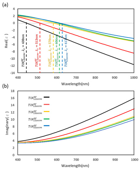
Figure 1.
(a) Real part and (b) imaginary part of permittivity ε of titanium nitride (TiN) films deposited at various N2 flow rates without bias.
Figure 2 plots the permittivity as a function of wavelength for samples deposited at a bias of 100 V. The variation of permittivity with the N2 flow rate is a reverse of that of the samples that were deposited under no bias. The real part of the permittivity as a function of wavelength indicates that the cross wavelength λc decreased from 576 nm to 451 nm as the flow rate of nitrogen increased from 1.2 sccm to 3.5 sccm. Unlike in the case with no bias, increasing the N2 flow rate made the real permittivity more negative at wavelengths larger than the cross wavelengths and the imaginary permittivity lower. At a wavelength of 800 nm, the real part of the permittivity varied from −2.2 to −15.6 as the N2 flow rate increased from 1.2 sccm to 3.5 sccm. At an N2 flow rate of 3.5 sccm, the sample had the most negative real part of the permittivity, which varied from zero at a wavelength of 451 nm to −25.5 at a wavelength of 1000 nm, which is similar to that of gold. Accordingly, increasing the N2 flow rate and substrate bias increased the magnitude of the negative real permittivity. These opposite variations of the permittivities of the two sets of TiN films also appear in the variations of morphologies. Figure 3 presents top-view images of uniform TiN films. For the TiN films that were deposited with bias, the crystallite structure becomes obvious at a low rate of N2 flow [20]. However, for the TiN films that were deposited without bias, the crystallite phenomenon was obvious at a high rate of N2 flow [21]. From the SEM images, the thickness is proportional to the porosity of thin film. The influence of the N2 flow rate and the bias voltage on the nanostructure of TiN film results in the deposition rate variation.
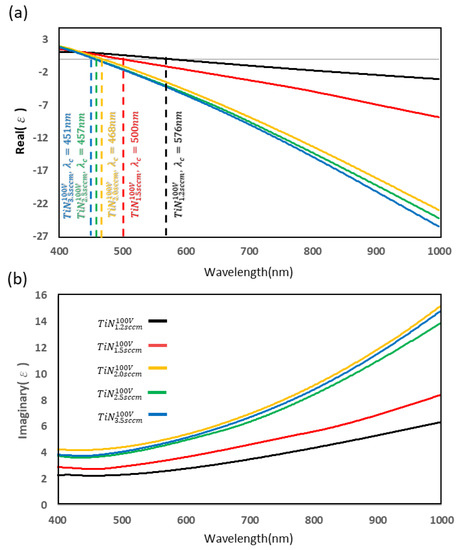
Figure 2.
(a) Real part and (b) imaginary part of permittivity ε of TiN films deposited at various flow rates with bias.
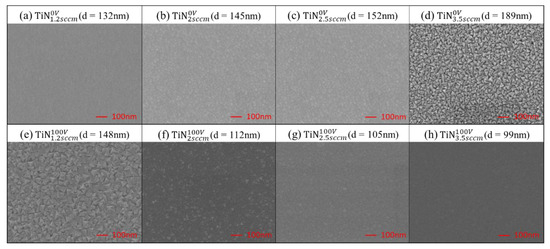
Figure 3.
Top-view images of TiN films deposited (a–d) with bias and (e–f) without bias at different N2 flow rates.
Figure 4 shows the grazing incidence X-ray diffraction (GIXRD) patterns of TiN samples. It is clear that the films deposited with bias exhibit (200) peaks. The (200) peak has an influence on the resistivity of TiN films. The TiN films with a (200) preferred orientation have lower resistivity than those with a (111) preferred orientation [22]. The influence of bias on the permittivity is obvious for TiN films deposited at the N2 flow rates larger than 2 sccm. The three metal-like permittivity spectra of samples , , and are similar. According to a previous work [20], increasing nitrogen flow rate would increase the composition ratio of N/Ti to approach unity. On the other hand, the additional substrate bias used at the lower temperature deposition resulted in a higher ratio of N bounded to Ti and a lower concentration of oxygen impurities [16].
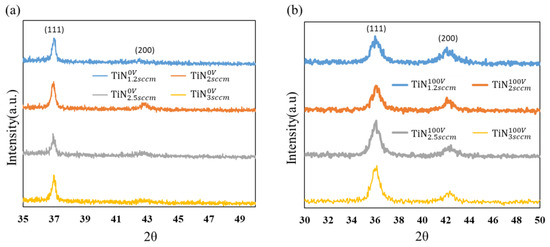
Figure 4.
Grazing incidence X-ray diffraction (GIXRD) patterns of TiN films deposited at various N2 flow rates (a) without bias (b) with bias.
3. TiN Nanorod Arrays: Fabrication and Measurement
The BK7 glass substrate was tilted at a deposition angle of 86° to perform GLAD under the same deposition conditions as in the aforementioned fabrication of uniform TiN films. A quartz monitor was mounted next to the substrate to record the deposition rate. The deposition rates of samples in N2 flow rates of 1.2 sccm and 3.5 sccm were fixed at 0.9 A/s and 0.4 A/s, respectively. Two sets of TiN NRA were grown with similar thicknesses, ranging from 157 to 173 nm. The first set was the three TiN NRAs deposited with substrate biases of 0 V, 50 V, and 100 V for an N2 flow rate of 1.2 sccm. The second set was the three TiN NRAs deposited at N2 flow rates of 1.2 sccm, 1.5 sccm, and 3.5 sccm without substrate bias. Figure 5 presents top-view and cross-sectional images of all samples. Each TiN NRA had a vertical thickness of d, an average tilt angle of rods of β, an average length of rods of l, and an average rod diameter of D, as shown in Table 1 and Table 2. From the top view of SEM, the rod tops emerge at the surface with triangular facets. The surface topography of the films is less influenced by the flow rate of nitrogen for the case without bias. It is clear that as the bias voltage increases from 0 V to 100 V, the average size of triangular facets corresponding to the (111) texture is reduced. The samples that were deposited under an applied bias had a lower tilt angle β than the samples deposited without a bias. The rod diameter increased with the film thickness as a result of the fanning-out phenomenon. The fanning-out phenomenon is caused during obliquely deposition. The width of nanorods are increased along the direction perpendicular to the growth direction of nanorods [23].
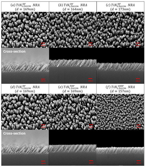
Figure 5.
Top-view and cross-sectional images of the TiN nanorod arrays (NRAs) deposited (a–d) without bias and (e–f) with bias at different N2 flow rates.

Table 1.
The morphology parameters of TiN NRAs deposited at a flow rate of 1.2 sccm with different bias.
Table 2.
The morphology parameters of TiN NRAs deposited at a different flow rates without bias.
Table 3 shows the composition of Ti and N measured with energy-dispersive X-ray spectroscopy (EDS). The result shows a high nitrogen concentration, with a Ti:N ratio of approximately 20:80. For samples , , and , the concentration of N decreases with increasing negative bias voltage. This phenomenon is due to the following [24,25]. Increasing negative bias voltage enhances the bombarding energy of the Ar+ ions on the substrate. In addition, the TiN film is overstoichiometric, which means that more N atoms are located at the grain boundaries to be resputtered easily. For samples , , and , the increase in concentration of N is related to the increase in the N2 flow rate.
Table 3.
Composition of Ti and N of TiN NRAs.
The s-polarized and p-polarized extinctance E spectra of those TiN NRAs were derived by measuring the reflectance R and transmittance T of each sample as functions of wavelength λ and angle of incidence θ using a Hitachi 4150 spectrophotometer. The extinctance E is given by 1-R-T, as shown in Figure 6. The extinctance versus angle of incidence was measured every ten degrees from θ = −70° to θ = 70°. However, in order to detect the LPM resonance precisely, the extinctance was measured every two degrees over the range of wavelength between 600 nm and 900 nm and the range of angle between θ = −46° and θ = −60°. The plane of incidence was set to be coincident with the plane that contained the normal surface and the direction of growth of the nanorods. The angle of incidence, θ, was defined as negative or positive as shown in Figure 6. For s-polarization, the extinctance is largest at the shortest wavelength of 400 nm and the high extinction is sustained over a wide range of incident angles. The strong s-polarized extinction corresponds to the transverse mode of surface plasmon resonance in those rods.
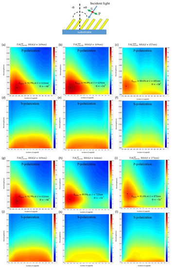
Figure 6.
P-polarized and s-polarized extinctance spectra of TiN NRAs: (a,d); (b,e) ; (c,f) ; (g,j); (h,k) ; (i,l) .
For p-polarization, since the slanted nanorods lie at an angle with respect to the oscillating electric file, the electric field has components along and perpendicular to the nanorods. Therefore, the p-polarized extinctance is dominated by both LPM and TPM. When the LMP is excited at wavelengths longer than 700 nm, the two maxima associated with LPM and TPM become obvious. Figure 7 shows the p-polarized spectra of and measured at normal incidence, the maxima at the wavelength of 400 nm corresponds to TPM. The maxima at wavelengths of 664 nm and 817 nm correspond to the LPM of , and , respectively. As with the s-polarized extinctance spectra, the TPM resonance is also excited by the electric field component perpendicular to the rods. Therefore, the p-polarized extinctance present strong and wide-angle extinction at short wavelengths. The other extinctance maximum corresponding to the LPM is close to the direction in which the oscillating electric field is parallel to the rods. The first set shows that the wavelength corresponding to the LPM maximum extinctance increases from 616 nm, 624 nm, to 681 nm as the bias increases from 0 V, 50 V, to 100 V, respectively. The maximum extinctance values are 92.9%, 94.8%, and 80.6% for samples deposited at 0 V, 50 V, and 100 V, respectively. For the NRA, the maximum extinctance occurs at θ = −58°that is higher than that of NRA (θ = −48°). The reason for the resonant angle shift is that the tilt angle β of NRA is lower than that of NRA, so the incident wave needs a higher θ to have the electric field oscillating along the rods. The spectra show that increasing the bias voltage significantly redshifts the resonant wavelength.
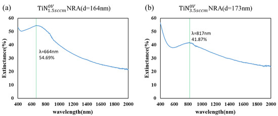
Figure 7.
P-polarized extinctance spectra of (a) and (b) at normal incidence.
The second set shows that the maximum extinctance values are 92.9%, 94.8%, and 80.6% at wavelengths of 616 nm, 725 nm, to 876 nm for samples deposited at the N2 flow rates of 1.2 sccm, 1.5 sccm, to 3.5 sccm, respectively. Clearly, increasing the N2 flow rate significantly redshifts the resonant wavelength. Figure 8 shows the sample NRA, increasing the thickness from 169 nm to 222 nm causes the LPM maximum extinctance to change from 92.9% at a wavelength of 616 nm to 96.61% at a wavelength of 607 nm, respectively. The thickness dependent plasmonic resonance of TiN NRA can be seen as similar to the way in which a variation in the thickness of a silver NRA only slightly changes the maximum resonant wavelength [11]. The redshift phenomena of both sets come from the permittivity of TiN NRA which varies with deposition parameters. Increasing the N2 flow rate without bias or increasing the bias under a constant bias voltage would lead to a metal-like permittivity, as shown in Figure 1 and Figure 2. The TiN NRA with a high metal-like permittivity has a shorter LPM resonant wavelength than that with a low metal-like permittivity.
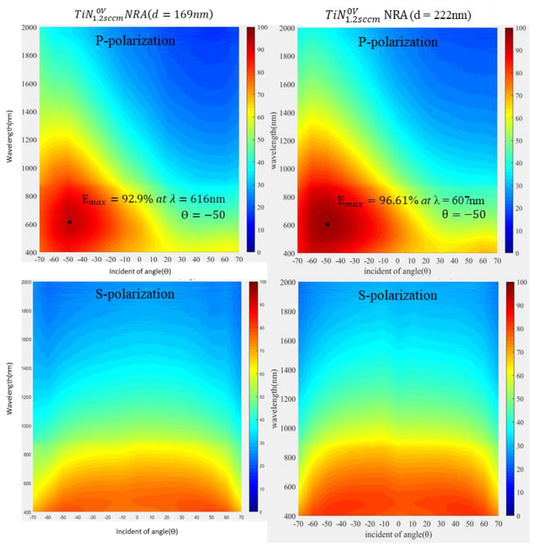
Figure 8.
S-polarized and p-polarized extinctance spectra of NRAs with different thickness.
4. Near-Field Simulation for LPM Resonance
The permittivity dependent LPM and TPM resonances are verified here with a near-field simulation. The finite-difference time-domain (FDTD) method is used to examine the variation of the localized field enhancement with the wavelength. High extinction of a nanostructured thin film indicates strong light coupling into the localized surface plasmon resonance [26]. The near field FDTD simulation was adopted to estimate the wavelength where strong local field intensity occurs and compare it with the far filed extinctance spectrum. The electric field profiles of the TiN NRAs that were illuminated by p-polarized light waves were simulated using FDTD software (FDTD Solutions 8.11.337, Vancouver, BC V6E 2M6, Canada). The following parameters were used in the simulations: FDTD cell size ∆x = ∆y = ∆z = 2 nm and time step ∆t = 0.95/c(∆x2 + ∆y2 + ∆z2)1/2, where c is the speed of light, chosen based on the Courant stability criterion. The (x, y, z) coordinate system is oriented as shown in Figure 9. The morphology of the deposited NRA with a thickness of 169 nm is adopted here for simulation. The same morphology of NRA is also adopted for NRA in simulation because both samples have similar morphologies. The p-polarized wave was on the NRA at an angle of incidence of θ = −50∘and the wavelength varied from 400 nm to 900 nm. The permittivity of TiN is that of the uniform TiN film, which was deposited under the same conditions.
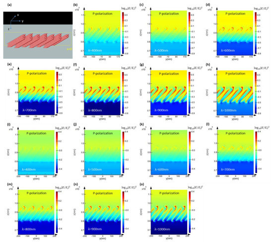
Figure 9.
(a) Schematic of the TiN NRA used in the simulation. Electric filed intensity distributions of (b–h) NRAs and (i–o) NRAs under p-polarized illumination at wavelengths from 400 nm to 1000 nm.
The distributions of electric field intensity on the cross section y-z plane are shown in Figure 9. In both cases, the local field enhancement corresponding to the LPM resonance is observed. The field intensity of the NRA is less than that of the NRA at the same wavelength, which is in agreement with the fact that the measured extinctance of the NRA is less than that of the NRA, as shown in Figure 6. For the NRA, the local field intensity becomes strong at wavelengths larger than 600 nm. However, the other local field intensity of the NRA becomes strong at wavelengths larger than 700 nm. The redshift of the wavelength is qualitatively in agreement with the measured redshift of the maximum extinctance, as shown in Figure 6. It can be concluded that the main cause of the redshift is the variation in the permittivity tuned by controlling the flow rate of N2 during deposition. More negative permittivity of TiN yields a shorter resonant wavelength.
5. Conclusions
The tunable optical property of TiN was exploited to tune the plasmon resonance of TiN nanorods. The dependence of the permittivity of deposited TiN film on the N2 flow rate without bias is the opposite of that with an applied bias. The associated longitudinal resonant wavelength was shifted by varying the N2 flow rate. The additional bias during deposition changed the tilt angle of nanorods with respect to the normal surface. The proposed method can be used not only to tune the resonant wavelength, but also to keep the extinctance high. As well as changing the morphology of the nanoparticles, plasmonic resonance can be varied by changing the deposition parameters. It gives more flexibility in the design of various nanoplasmonic structures, favoring applications that are based on light–matter interactions.
Author Contributions
Y.-J.J. conceived the idea and supervised the whole work. Z.-X.L., W.-C.L. and M.-Y.C. deposited the films and performed measurements. Y.-J.J., Z.-X.L., B.-H.L., and T.-L.C. analyzed the data. Y.-J.J. wrote the article. Y.-J.J., B.-H.L. and T.-L.C. revised the paper.
Funding
This research was funded by the Ministry of Science and Technology of the Republic of China, Taiwan, for financially supporting this research under contract MOST108-2221-E-027-100-MY3.
Conflicts of Interest
The authors declare no conflict of interest.
References
- Stefan, A. Maier, Plasmonics: Fundamentals and Applications; Springer Science & Business Media: New York, NY, USA, 2007. [Google Scholar]
- Jia, H.; Liu, H.; Zhong, Y. Role of surface plasmon polaritons and other waves in the radiation of resonant optical dipole antennas. Sci. Rep. 2015, 5, 8456. [Google Scholar] [CrossRef] [PubMed]
- Atwater, H.A.; Polman, A. Plasmonics for improved photovoltaic devices. Nat. Mater. 2010, 9, 205–213. [Google Scholar] [CrossRef] [PubMed]
- Ren, M.; Jia, B.; Ou, J.Y.; Plum, E.; Zhang, J.; MacDonald, K.F.; Zheludev, N.I. Nanostructured plasmonic medium for terahertz bandwidth all-optical switching. Adv. Mater. 2011, 23, 5540–5544. [Google Scholar] [CrossRef] [PubMed]
- Dani, K.M.; Ku, Z.; Upadhya, P.C.; Prasankumar, R.P.; Brueck, S.R.J.; Taylor, A.J. Subpicosecond optical switching with a negative index metamaterial. Nano Lett. 2009, 9, 3565–3569. [Google Scholar] [CrossRef] [PubMed]
- Zhou, Z.; Liu, J.; Bao, Y.; Wu, L.; Png, C.E.; Wang, X.; Qiu, C. Quantum plasmonics get applied. Prog. Quantum Electron. 2019, 65, 1–20. [Google Scholar] [CrossRef]
- Jen, Y.J.; Huang, J.W.; Liu, W.C.; Chan, S.; Tseng, C.H. Glancing angle deposited gold nanohelix arrays on smooth glass as three-dimensional SERS substrates. Opt. Mater. Express 2016, 6, 697–704. [Google Scholar] [CrossRef]
- Yi, Z.; Niu, G.; Chen, J.; Luo, J.; Liu, X.; Yi, Y.; Tang, Y. Dipole, quadrupole, and octupole plasmon resonance modes in ag nanoring structure: Local field enhancement in the visible and near infrared regions. Plasmonics 2016, 11, 37–44. [Google Scholar] [CrossRef]
- Haes, A.; Van Duyne, R.P. A unified view of propagating and localized surface plasmon resonance biosensors. Anal. Bioanal. Chem. 2004, 379, 920–930. [Google Scholar] [CrossRef]
- Ringe, E.; Langille, M.R.; Sohn, K.; Zhang, J.; Huang, J.; Mirkin, C.A.; Marks, L.D. Plasmon length: A universal parameter to describe size effects in gold nanoparticles. J. Phys. Chem. Lett. 2012, 3, 1479–1483. [Google Scholar] [CrossRef]
- Zhao, Y.-P.; Chaney, S.B.; Zhang, Z.-Y. Absorbance spectra of aligned Ag nanorod arrays prepared by oblique angle deposition. J. Appl. Phys. 2006, 100, 063527. [Google Scholar] [CrossRef]
- Boltasseva, A.; Atwater, H.A. Low-loss plasmonic metamaterials. Science 2011, 331, 290–291. [Google Scholar] [CrossRef] [PubMed]
- Guler, U.; Boltasseva, A.; Shalaev, V.M. Refractory plasmonics. Science 2014, 344, 263–264. [Google Scholar] [CrossRef] [PubMed]
- Guler, U.; Naik, G.V.; Boltasseva, A.; Shalaev, V.M.; Kildishev, A.V. Performance analysis of nitride alternative plasmonic materials for localized surface plasmon applications. Appl. Phys. B Lasers Opt. 2012, 107, 285–291. [Google Scholar] [CrossRef]
- Guler, U.; Kildishev, A.V.; Boltasseva, A.; Shalaev, V.M. Plasmonics on the slope of enlightenment: The role of transition metal nitrides. Faraday Discuss 2015, 178, 71–86. [Google Scholar] [CrossRef] [PubMed]
- Zgrabik, C.M.; Hu, E.L. Optimization of sputtered titanium nitride as a tunable metal for plasmonic applications. Opt. Mater. Express 2015, 5, 2786–2797. [Google Scholar] [CrossRef]
- Jen, Y.J.; Wang, W.C.; Wu, K.L.; Lin, M.J. Extinction properties of obliquely deposited TiN nanorod arrays. Coatings 2018, 8, 465. [Google Scholar] [CrossRef]
- Robbie, K.; Brett, M.J. Sculptured thin films and glancing angle deposition: Growth mechanics and applications. J. Vac. Sci. Technol. A Vac. Surf. Film. 1997, 15, 1460. [Google Scholar] [CrossRef]
- Xi, J.Q.; Schubert, M.F.; Kim, J.K.; Schubert, E.F.; Chen, M.; Lin, S.Y.; Smart, J.A. Optical thin-film materials with low refractive index for broadband elimination of Fresnel reflection. Nat. Photonics 2007, 1, 176–179. [Google Scholar] [CrossRef]
- Huang, J.H.; Lau, K.W.; Yu, G.P. Effect of nitrogen flow rate on structure and properties of nanocrystalline TiN thin films produced by unbalanced magnetron sputtering. Surf. Coat. Technol. 2005, 191, 17–24. [Google Scholar] [CrossRef]
- Arshi, N.; Lu, J.; Joo, Y.K.; Lee, C.G.; Yoon, J.H.; Ahmed, F. Influence of nitrogen gas flow rate on the structural, morphological and electrical properties of sputtered TiN films. J. Mater. Sci. Mater. Electron. 2013, 24, 1194–1202. [Google Scholar] [CrossRef]
- Sun, N.; Zhou, D.; Shi, S.; Liu, W.; Zhao, X.; Liu, F.; Tian, Z.; Li, S.; Wang, J.; Ali, F. DC substrate bias enables preparation of superior-performance TiN electrode films over a wide process window. Mater. Res. Bull. 2019, 119, 110575. [Google Scholar] [CrossRef]
- Dhruv, P.S.; Goel, P.; Singh, J.P. Revisiting the structure zone model for sculptured silver thin films deposited at low substrate temperatures. J. Appl. Phys. 2012, 112, 104324. [Google Scholar]
- Choi, J.; Jeon, W.; Kang, D.; Kang, D.; Jo, J. Hydrogen-assisted sputtering growth of TiN on ceramic substrates. Coatings 2019, 9, 255. [Google Scholar] [CrossRef]
- Chun, S.Y. Bias voltage effect on the properties of TiN films by reactive magnetron sputtering. J. Korean Phys. Soc. 2010, 56, 1134–1139. [Google Scholar] [CrossRef]
- Jen, Y.J.; Huang, Y.J.; Liu, W.C.; Lin, Y.S.W. Densely packed aluminum-silver nanohelices as an ultra-thin perfect light absorber. Sci. Rep. 2017, 7, 39791. [Google Scholar] [CrossRef] [PubMed]
© 2019 by the authors. Licensee MDPI, Basel, Switzerland. This article is an open access article distributed under the terms and conditions of the Creative Commons Attribution (CC BY) license (http://creativecommons.org/licenses/by/4.0/).