Article

Influence of Annealing Temperature on the Properties of ZnGa2O4 Thin Films by Magnetron Sputtering

1
Department of Materials Science and Engineering, Da-Yeh University, Changhua 51591, Taiwan
2
Graduate Institute of Materials Science and Green Energy Engineering, National Formosa University, Huwei, Yunlin 632, Taiwan
3
Department of Industrial Engineering and Management, Da-Yeh University, Changhua 51591, Taiwan
*
Author to whom correspondence should be addressed.
Coatings 2019, 9(12), 859; https://doi.org/10.3390/coatings9120859
Submission received: 16 November 2019 / Revised: 9 December 2019 / Accepted: 11 December 2019 / Published: 14 December 2019

Abstract

:
Zinc gallate (ZnGa2O4) thin films were grown on sapphire (0001) substrate using radio frequency (RF) magnetron sputtering. After the thin film deposition process, the grown ZnGa2O4 was annealed at a temperature ranging from 500 to 900 °C at atmospheric conditions. The average crystallite size of the grown ZnGa2O4 thin films increased from 11.94 to 27.05 nm as the annealing temperature rose from 500 to 900 °C. Excess Ga released from ZnGa2O4 during thermal annealing treatment resulted in the appearance of a Ga2O3 phase. High-resolution transmission electron microscope image analysis revealed that the preferential crystallographic orientation of the well-arranged, quasi-single-crystalline ZnGa2O4 (111) plane lattice fringes were formed after the thermal annealing process. The effect of crystallite sizes and lattice strain on the width of the X-ray diffraction peak of the annealed ZnGa2O4 thin films were investigated using Williamson-Hall analysis. The results indicate that the crystalline quality of the deposited ZnGa2O4 thin film improved at higher annealing temperatures.

1. Introduction

Zinc gallate (ZnGa2O4) belongs to a group of close-packed, face-centered cubic structured compounds (AB2O4) with a normal oxide spinel structure (space group of Fd3m). Zn2+ and Ga3+ cations occupy the tetrahedrally coordinated A-sites in tetrahedral and octahedral lattice B-sites, respectively. The lattice constant is 8.334 Å at room temperature [1]. ZnGa2O4 materials have recently gained increased attention [2,3]. These materials are widely applied in vacuum fluorescent and field emission displays, gas sensors, electronic devices, and solar-blind ultraviolet photodetectors (PDs) due to their high transparency in the deep ultraviolet (DUV) spectral region, excellent thermal and chemical stability, and wide optical band gap (~5 eV) [4,5,6].
Researchers have discussed many one-dimensional (1D) ZnGa2O4 nanostructures (nanoparticles, nanocrystal, nanowires, and nanotube) over the years [7,8,9]. Although these 1D ZnGa2O4 devices exhibit high optoelectronic performance, the reliability and stability of these devices are a critical aspect of their application, which raises concern [10,11]. Thin film structures have been proven to possess properties that can overcome the aforementioned challenges posed by a 1D ZnGa2O4 nanostructure. Therefore, it is important to develop and perfect ZnGa2O4 film materials and related optoelectronic devices.
There are several methods for the preparation of ZnGa2O4 thin films, including: sol-gel [12], pulsed laser deposition [13], metalorganic chemical vapor deposition (MOCVD) [14], and radio frequency (RF) magnetron sputtering [15]. Shen et al. used ZnGa2O4 thin film for the development of metal-oxide-semiconductor field effect transistors by MOCVD. Their research showed promising results in enhancing the breakdown voltage and Ion/Ioff (current on/off) ratio performance [16]. Wu et al. reported that the properties of thin film ZnGa2O4 gas sensor deposited by MOCVD [17]. Huang et al. developed a ZnGa2O4 thin film solar-blind PDs based on a metal-semiconductor-metal structure fabricated by an RF magnetron sputtering method [18]. They investigated the effect of oxygen partial pressure on the electrical properties of the devices during the sputtering and thermal annealing process.
Among these growth techniques, RF magnetron sputtering techniques have many advantages, including the ease of controlling the growth parameter, excellent packing density, good adhesion, and relatively low running cost. However, the RF magnetron sputtering method often produces amorphous or polycrystalline film structures that significantly destroy the optical and electrical properties of the material. Enhancement of polycrystalline thin films has spurred several types of research, leading to the investigation of process parameters that include growth temperature, film thickening, post-annealing temperature, and RF power. In this paper, the effects of post-annealing temperatures on the structural and optical properties of ZnGa2O4 films deposited on sapphire substrates after RF magnetron sputtering were investigated.

2. Experimental Methods
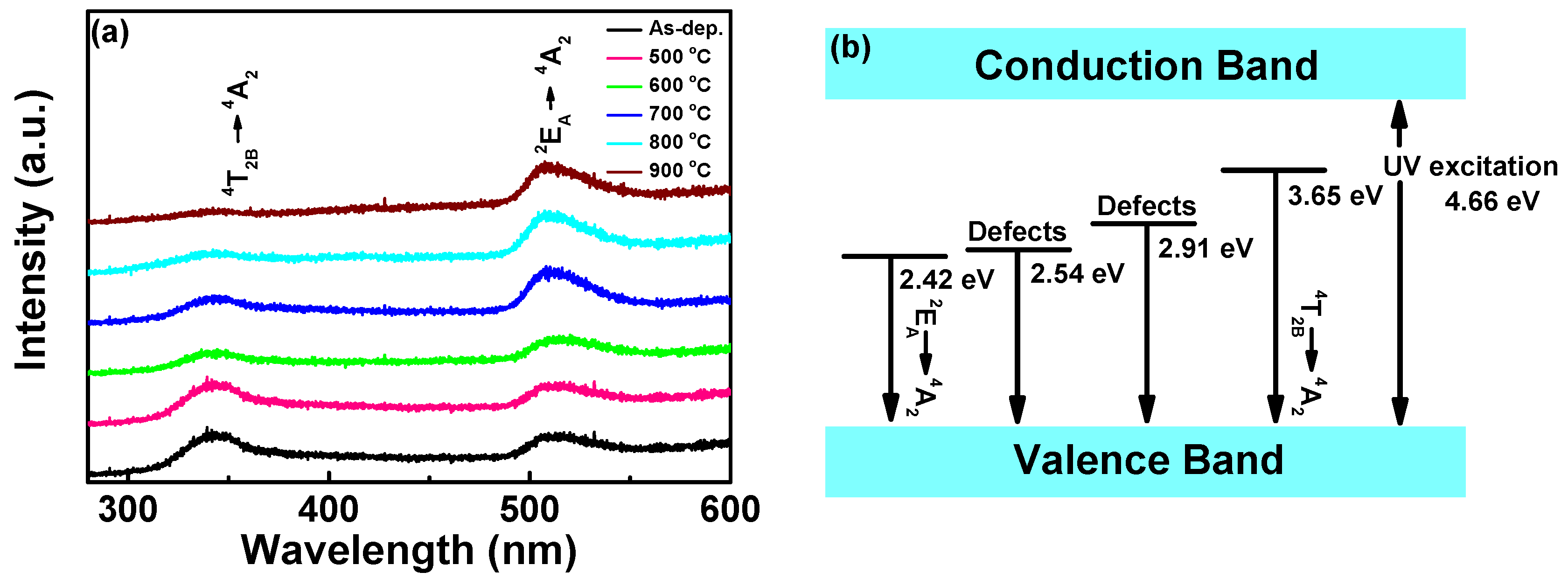
The ZnGa2O4 thin films were deposited over a C-plane sapphire using the RF magnetron sputtering technique. The sputtering target was ZnGa2O4 ceramic, which was sintered with ZnO and Ga2O3 powder of 99.99% purity, with a mix proportion of 30:70. Initially, the substrates were cleaned in acetone and alcohol, followed by ultrasonic cleansing in de-ionized water for 10 min, and then blow-dried with nitrogen gas. Prior to deposition, the vacuum level of chamber pressure was approximately 5 × 10⁻⁶ torr. The plasma generation was activated by the RF power for ZnGa2O4, the target was 150 W at 13.56 MHz, and the deposition pressure was kept at 5 × 10⁻³ torr. The as-deposited film was deposited at the substrate temperature of 400 °C. The distance between target and the substrate was 15 cm. To maintain uniform film thickness, the substrate holder was rotated at 18 rpm during the deposition process. The deposition time was 2 h and the deposited samples were annealing at different temperature ranging from 500 to 900 °C in steps of 100 °C at atmospheric ambient conditions in a quartz furnace tube. The crystallographic properties of ZnGa2O4 films were investigated by X-ray diffraction (XRD, X’Pert PRO MRD, PANalytical, Almelo, The Netherlands) with Cu Kα X-ray source (λ = 1.541874 Å) radiation. The surface morphologies, microstructures, and elemental analyses of these deposited samples were analyzed by scanning electron microscopy (SEM, S-3000H, Hitachi, Tokyo, Japan), atomic force microscopy (AFM, 5400, Agilent, Santa Clara, CA, USA), and high-resolution transmission electron microscopy (HRTEM, H-600, Hitachi, Tokyo, Japan). Optical properties (transmittance, absorbance, and photoluminescence) were determined using an UV-visible (UV-VIS) near infra-red (NIR) spectrophotometer (Model: LAMBDA 750 from Perkin Elmer, Perkin Elmer, MA, USA).

3. Results

The XRD spectra of the deposited ZnGa2O4 thin films as a function of annealing temperature is shown in Figure 1a. The annealing temperature was varied from 500 to 900 °C for 1 h. The polycrystalline nature of all the deposited ZnGa2O4 film can be indexed and refer to the reported data of Joint Committee on Powder Diffraction Standards (JCPDS) card file 38-1240; the characteristic peaks of the preferred crystallographic orientations are (220), (311), (222), (400), (511), and (440). The intensity of the diffraction peak (311) plane increased with an increase in the annealing temperature. The increment of the diffraction peak (311) is attributed to improved crystallinity of deposited ZnGa2O4 thin films. The diffraction peaks of Ga2O3 (−401) and (−202) were observed from the phase separation of ZnGa2O4 for the sample annealed at a temperature above 800 °C (Figure 1b). The JCPDS data of the Ga2O3 (card No. 43-1012) is given for reference. The observed Ga2O3 plane is attributed to the expulsion of Zn atoms at an annealing temperature above 800 °C [19]. The Debye-Scherrer formula in Equation (1) below was used to calculate the average crystallite size and full width at half maxima (FWHM) of ZnGa2O4 peak (311) at different annealing temperatures, as shown in Figure 1c [20]:
D = 0.9λ/βcos θ
where D is the average crystallite size (nm), λ is the wavelength of X-ray (0.15418 nm), β is the FWHM (radian), and θ is diffraction angle (degrees). The average crystallite sizes estimated by the Scherrer method increase from 11.94 to 27.05 nm. ZnGa2O4 crystallite size increased with an increase in annealing temperatures, and a narrower FWHM peak (311) was observed, indicating an improvement in the crystallinity of ZnGa2O4 (Figure 1c). The observation might be due to the enhanced nucleation dynamics and/or strain release. Based on the solid-state diffusion process, either the aggregation of small grains to form larger ones, or grain boundary movement, results in grain recrystallization and regrowth. This improved the crystallinity of ZnGa2O4 film at high annealing temperatures [21].
Figure 1d shows the variation of XRD peak intensity (311) and dislocation density with increased annealing temperatures. The value of the dislocation density (δ), which is related to the number of defects in the grown nanocrystalline film, was calculated from the average values of the crystallite size by the relationship in Equation (2) [22]:
δ = 1/D2
The dislocation density decreases as the annealing temperature increases, resulting in a decrement in the nature of native imperfections (defects, concentration of native impurity, and stress) at high annealing temperatures [23]. The Williamson-Hall analysis was used to evaluate the crystalline sizes and lattice strain distribution in the sample. This can be determined by Equation (3) [24]. The calculated parameters are shown in Table 1.
βhklcos (θhkl) = kλ/DW-H + 4εsin (θhkl)
where ε is the lattice strain, k is the shape factor, and (hkl) is the Miller Indices. Other parameters have previously been defined in Equation (1). The strain in the ZnGa2O4/sapphire samples at different annealing temperatures can be calculated from the slope of plotted of βhklcos θhkl (along the y-axis) and sin θ (along the x-axis) as shown in Figure 2a–f. The slopes of the fitted trendline for each plot (Figure 2a–e) were negative, indicating the existence of compressive strain in the lattice of all ZnGa2O4/sapphire samples. The intrinsic compressive stresses observed in the sputtering method deposited films were mainly caused by energetic particle bombardment, lattice mismatch, defects, etc. of the depositing films/substrate. After the sample was annealed at 900 °C, a positive slope was observed, which indicates the existence of tensile strain in the lattice (Figure 2f) [25].
Plane-view SEM images of the ZnGa2O4 films at different annealing temperatures are shown in Figure 3a–f. It can be seen that the surface morphologies of these ZnGa2O4 films exhibit a very similar column structure. As the annealing temperature increases, the crystallite size increases. The increment is caused by regrowth and coalescence during thermal treatment. Moreover, a high annealing temperature provides sufficient driving force to improve the mobility of the atoms, and further improve the film crystallinity. These results are in agreement with the observation from the XRD spectra. It can be concluding that the crystallinity of the films can be improved by controlling annealing temperature. Similar results have been reported by Sharma et al. [26].
The surface morphologies of the ZnGa2O4 films at various annealing temperatures were obtained by AFM, as shown in Figure 4. The root mean square (RMS) values of the annealed samples (500, 600, and 700 °C) decreased compared to that of the as-deposited sample. As the annealing temperature increased above 800 °C, the RMS increased from 3.228 to 3.549 nm. This can be attributed to the phase separation that occurred at the surface resulting from the thermal decomposition or atomic migration on the disordered nanostructure of the ZnGa2O4 film. Figure 5a shows the cross-sectional transmission electron microscopy (TEM) images of ZnGa2O4 film annealed at a temperature of 900 °C. It was found that the ZnGa2O4 film exhibited a columnar structure with a thickness of approximately 485 nm. To investigate the detailed microstructure and compositional distribution of annealed ZnGa2O4 films, zones I, II, and III in Figure 5a were further analyzed by HRTEM. D-spacing was used to define the distance between planes of atoms in crystalline materials. Nanocrystalline grains including the crystal planes of ZnGa2O4 (311) and Ga2O3 (−401) were observed (Figure 5b), which corresponded to a d-spacing of 2.5 and 2.9 Å, respectively. This is because Zn atoms diffuse from the film at high annealing temperatures resulting in the partial conversion of ZnGa2O4 to Ga2O3. Therefore, it can be inferred that the Ga2O3 phases are accompanied by ZnGa2O4 phases in this layer. Multiple phases including ZnGa2O4 (311), (222), (400), and (220) plane were obtained, as shown in Figure 5c. The clear crystal lattice stripes with the preferred orientation perpendicular to the film surface of cubic ZnGa2O4 (111) (d-spacing value of 4.8 Å) possess a quasi-single-crystalline structure (Figure 4d). This result might be attributed to the thermally activated process that provides enough kinetic energy, which was imparted to the ZnGa2O4 molecules. The imparted kinetic energy aids the rearrangement and improvement of crystallite perfection in the ZnGa2O4 thin film structure.
The optical transmittance spectra and energy gap of ZnGa2O4 films annealed at different temperatures are shown in Figure 6. The optical transmittance spectra of ZnGa2O4 thin films were recorded from 200 to 1000 nm. All deposited ZnGa2O4 films showed high transmittance greater than 80% in the ultraviolet A radiation UVA (400–315 nm) and ultraviolet B radiation (UVB) (315–280 nm) regions. The decrease may be attributed to a rough surface, as observed in the AFM result. The energy gap of ZnGa2O4 thin films at annealing temperatures ranging from 500 to 900 °C can be evaluated from the absorption edge (αhν)2 curve as shown in Figure 6b [27], where α is the absorption coefficient and hν is the photon energy. The photon energy gap increased from 4.7 eV for the as-deposited sample to 4.98 eV as the annealing temperature increased to 900 °C. The increase in energy gap is attributed to the decrease in the number of defect densities and grain boundaries, as well as the increase in the annealing temperature. The energy gap is narrowed because the amorphous structure usually produces excited electrons that undergo conduction in defect state [28].
The photoluminescence emission spectra of ZnGa2O4 thin films at various annealing temperature is shown in Figure 7a. It was observed that the sample under higher annealing temperatures has a higher luminescence intensity. While all of the annealed samples of photoluminescence spectra exhibited broad band emission extending from 300 to 600 nm, the emission peaks were located at 340 and 520 nm. The emission peak centered at 340 nm can be attributed to the 4T2B4T2A transition, while the 2EA4T2A transition is responsible for the emission peak centered at 520 nm. Since the UV band emission is related to the excited excess Ga3+ ions of the Ga–O group [29]. During thermal annealing, the Ga3+ ions substitute the Zn2+ ions site in the AB2O4 spinel structure, then interactions between the p orbitals in the Ga3+ ion and the orbitals of the six oxygen ligands lead to a shifts in the energy levels of the individual orbitals in a distorted octahedral configuration, further splitting the five 3d-orbital energy levels. The five 3d-orbital energy levels are labeled 4T1, 4T2A, 4T2B, 2EB, 2EA, and 4A2. A schematic diagram of the energy levels in ZnGa2O4 thin films is illustrated in Figure 7b. It was previously reported that ZnGa2O4 annealed at different temperatures may lead to transitions as a result of the stoichiometric variations in the composition of Ga/Zn [30]. The possibility of the expulsion of Zn atoms from the ZnGa2O4 matrix increases with an increase in the annealing temperature. Therefore, a variation in the Ga/Zn stoichiometry in ZnGa2O4 thin films will be observed.

4. Conclusions

In this study, ZnGa2O4 thin films were prepared on sapphire substrate using an RF sputtering technique. The polycrystalline nature of the randomly oriented ZnGa2O4 films was improved and converted to a quasi-single-crystalline structure through thermal annealing treatment. The stress of the deposited ZnGa2O4 thin films was transformed from compressive to tensile stress as the annealing temperature increased from 500 to 900 °C. The optical transmittance of ZnGa2O4 films was greater than 80% in the UVA and UVB regions, and the energy band gap increased with an increase in annealing temperature. These results indicate that the annealing process is an effective method for the improvement of ZnGa2O4 thin film crystallinity, and may obtain the preferred orientation.

Author Contributions

Conceptualization, W.-K.W.; Methodology, Y.-J.X., S.-Y.H., K.-F.L., P.-C.T. and W.-K.W.; Data Curation, Y.-J.X., K.-F.L. and W.-K.W.; Writing—Original Draft Preparation, Y.-J.X., K.-F.L. and W.-K.W.; Writing—Review and Editing, W.-K.W.

Funding

This research was funded by the Ministry of Science and Technology, Taiwan (No. 108-2221-E-212-007).

Acknowledgments

The authors wish to express their sincere gratitude for the technical support from the advanced Industry Technology Centre of National Chung Hsing University, Taiwan.

Conflicts of Interest

The authors declare no conflict of interest.

References

  1. Omata, T.; Ueda, N.; Ueda, K.; Kawazoe, H. New ultraviolet-transport electroconductive oxide, ZnGa2O4 spinel. Appl. Phys. Lett. 1994, 64, 1077–1078. [Google Scholar] [CrossRef]
  2. Tsai, S.H.; Shen, Y.C.; Huang, C.Y.; Horng, R.H. Deep-ultraviolet Schottky photodetectors with high deep-ultraviolet/visible rejection based on a ZnGa2O4 thin film. Appl. Surf. Sci. 2019, 496, 143670. [Google Scholar] [CrossRef]
  3. Lee, H.; Bark, C.W.; Choi, H.W. Fabrication and characterization of perovskite solar cells with ZnGa2O4 mixed TiO2 photoelectrode. Jpn. J. Appl. Phys. 2019, 58, SDDE15. [Google Scholar] [CrossRef] [Green Version]
  4. Horng, R.H.; Huang, C.I.; Ou, H.L.; Juang, T.K.; Liu, P.L. Epitaxial growth of ZnGa2O4: A new, deep ultraviolet semiconductor candidate. Cryst. Growth Des. 2017, 17, 6071–6078. [Google Scholar] [CrossRef]
  5. Jiao, Z.; Ye, G.; Chen, F.; Li, M.; Liu, J. The preparation of ZnGa2O4 nano crystals by spray coprecipitation and its gas sensitive characteristics. Sensors 2002, 2, 71–78. [Google Scholar] [CrossRef] [Green Version]
  6. Lee, Y.E.; Norton, D.P.; Budai, J.D.; Wei, Y. Enhanced ultraviolet photoconductivity in semiconducting ZnGa2O4 thin films. J. Appl. Phys. 2001, 90, 3863. [Google Scholar] [CrossRef]
  7. Kamal, C.S.; Boddu, S.; Vishwanadh, B.; Rao, K.R.; Sudarsan, V.; Vatsa, R.K. Blue luminescence from ZnGa2O4: Effect of lattice distortion and particle size. J. Lumin. 2017, 188, 429–435. [Google Scholar] [CrossRef]
  8. Liang, H.F.; Meng, F.; Lamb, B.K.; Ding, Q.; Li, L.S.; Wang, Z.C.; Jin, S. Solution growth of screw dislocation driven alpha-GaOOH nanorod arrays and their conversion to porous ZnGa2O4 nanotubes. Chem. Mater. 2017, 29, 7278–7287. [Google Scholar] [CrossRef]
  9. Hirano, M.; Okumura, S.; Hasegawa, Y.; Inagaki, M. Direct precipitation of spinel type oxide ZnGa2O4 from aqueous solutions at low temperature below 90 °C. Inorg. Mater. 2001, 3, 797–801. [Google Scholar] [CrossRef]
  10. Lou, Z.; Li, L.; Shen, G. High-performance rigid and flexible ultraviolet photodetectors with single-crystalline ZnGa2O4 nanowires. Nano Res. 2015, 8, 2162–2169. [Google Scholar] [CrossRef]
  11. Li, C.; Bando, Y.; Liao, M.; Koide, Y.; Golberg, D. Visible-blind deep-ultraviolet schottky photodetector with a photocurrent gain based on individual Zn2GeO4 nanowire. Appl. Phys. Lett. 2010, 97, 161102. [Google Scholar] [CrossRef]
  12. Hussen, M.K.; Dejene, F.B.; Gonfa, G.G. Effect of citric acid on material properties of ZnGa2O4:Cr3+ nanopowder by sol-gel method. Appl. Phys. A Mater. 2018, 124, 390. [Google Scholar] [CrossRef]
  13. Shi, Q.; Wang, C.Z.; Zhang, D.; Li, S.H.; Zhang, L.M.; Wang, W.J.; Zhang, J.Y. Luminescence of Cr3+ doped ZnGa2O4 thin films deposited by pulsed laser ablation. Thin Solid Film. 2012, 520, 6845–6849. [Google Scholar] [CrossRef]
  14. Lina, X.; Chen, D.; Niu, W.; Huang, C.Y.; Horng, R.H.; Cheng, L.C.; Talwar, D.N.; Lin, H.H.; Lee, J.F.; Feng, Z.C.; et al. Evolution of the local structure and crystal phase for thin ZnGaO films grown by metal organic chemical vapor deposition. J. Cryst. Growth 2019, 520, 89–95. [Google Scholar] [CrossRef]
  15. Wang, W.K.; Xu, Y.J.; Huang, S.Y.; Liu, K.F.; Tsai, P.C. Structural characteristics and photoluminescence properties of sputter-deposition ZnGa2O4 thin films on sapphire and Si(100) substrates. Coatings 2019, 9, 469. [Google Scholar] [CrossRef] [Green Version]
  16. Shen, Y.S.; Wang, W.K.; Horng, R.H. Characterizations of metal-oxide-semiconductor field-effect transistors of ZnGaO grown on sapphire substrate. IEEE J. Electron Devices Soc. 2017, 5, 112–116. [Google Scholar] [CrossRef]
  17. Wu, M.R.; Li, W.Z.; Tung, C.Y.; Huang, C.Y.; Chiang, Y.H.; Liu, P.L.; Horng, R.H. NO gas sensor based on ZnGa2O4 epilayer grown by metalorganic chemical vapor deposition. Sci. Rep. 2019, 9, 7459. [Google Scholar] [CrossRef]
  18. Huang, W.L.; Li, C.H.; Chang, S.P.; Chang, S.J. The Effect of oxygen partial pressure and annealing process on the characteristics of ZnGa2O4 MSM UV photodetector. ECS J. Solid State Sci. Technol. 2019, 8, Q3213–Q3216. [Google Scholar] [CrossRef] [Green Version]
  19. Yi, S.S.; Bae, J.S.; Moon, B.K.; Jeong, J.H.; Kim, I.W.; Park, H.L. Photoluminescence behavior of pulsed laser deposited ZnGa2O4 thin-film phosphors grown on various substrates. Appl. Phys. A 2003, 76, 433–437. [Google Scholar] [CrossRef]
  20. Chandolu, A.; Nikishin, S.; Holtz, M.; Temkin, H. X-ray diffraction study of AlN/AlGaN short period superlattices. J. Appl. Phys. 2007, 102, 114909. [Google Scholar] [CrossRef] [Green Version]
  21. Lee, J.Y.; Kim, H.S.; Chang, J.H.; Yang, M.; Ahn, H.S.; Ryu, S.O. Structural and luminescence characteristics of post-annealed ZnO films on Si (111) in H2O ambient. Jpn. J. Appl. Phys. 2005, 44, L205–L207. [Google Scholar] [CrossRef]
  22. Sharma, S.; Vyas, S.; Periasamy, C.; Chakrabarti, P. Structural and optical characterization of ZnO thin films for optoelectronic device applications by RF sputtering technique. Superlattices Microstruct. 2014, 75, 378–389. [Google Scholar] [CrossRef]
  23. Son, H.; Choi, Y.J.; Hwang, J.; Jeon, D.W. Influence of post-annealing on properties of α-Ga2O3 epilayer. ECS J. Solid State Sci. Technol. 2019, 8, Q3024–Q3027. [Google Scholar] [CrossRef]
  24. Zak, A.K.; Majid, W.H.A.; Abrishami, M.E.; Yousefi, R. X-ray analysis of ZnO nanoparticles by Williamson–Hall and size-strain plot methods. Solid State Sci. 2011, 13, 251–256. [Google Scholar]
  25. Somasundaram, K.; Abhilash, K.P.; Sudarsan, V.; Christopher Selvin, P.; Kadam, R.M. Defect luminescence and lattice strain in Mn2+ doped ZnGa2O4. Phys. B 2016, 491, 79–83. [Google Scholar] [CrossRef]
  26. Sharma, S.; Varma, T.; Asokan, K.; Periasamy, C.; Boolchandani, D. Annealing temperature dependent structural and optical properties of RF sputtered ZnO thin films. J. Nanosci. Nanotechnol. 2017, 17, 300–305. [Google Scholar] [CrossRef]
  27. Shi, F.F.; Han, J.; Xing, Y.H.; Li, J.H.; Zhang, L.; He, T.; Li, T.; Deng, X.U.; Zhang, X.D.; Zhang, B.H. Annealing effects on properties of Ga2O3 films deposited by plasma-enhanced atomic layer deposition. Mater. Lett. 2019, 237, 105–108. [Google Scholar] [CrossRef]
  28. Chen, P.W.; Huang, S.Y.; Yuan, S.H.; Chen, Y.A.; Hsiao, P.W.; Wuu, D.S. Quasi-single-crystalline ZnGa2O4 films via solid phase epitaxy for enhancing deep-ultraviolet photoresponse. Adv. Mater. Interfaces 2019, 6, 1901075. [Google Scholar] [CrossRef]
  29. Hsieh, I.J.; Chu, K.T.; Yu, C.F.; Feng, M.S. Cathodoluminescent characteristics of ZnGa2O4 phosphor grown by radio frequency magnetron sputtering. J. Appl. Phys. 1994, 76, 3735–3739. [Google Scholar] [CrossRef]
  30. Lee, Y.E.; Norton, D.P.; Park, C.; Rouleau, C.M. Blue photoluminescence in ZnGa2O4 thin-film phosphors. J. Appl. Phys. 2001, 89, 1653–1656. [Google Scholar] [CrossRef]
Figure 1. (a) XRD spectra of ZnGa2O4 films at different annealing temperatures; (b) XRD spectra of ZnGa2O4 showing a limited 2θ range (28° to 38°); (c) Effect of annealing temperature on the average crystallite size and FWHM of ZnGa2O4; (d) Effect of annealing temperature on the XRD peak intensity (311) and dislocation density.
Coatings 09 00859 g001
Figure 2. Williamson-Hall plot for ZnGa2O4 thin films annealed at temperature of (a) as-deposited, (b) 500 °C, (c) 600 °C, (d) 700 °C, (e) 800 °C, and (f) 900 °C.
Coatings 09 00859 g002
Figure 3. SEM micrographs of ZnGa2O4 thin film samples at different annealing temperatures of (a) as-deposited, (b) 500 °C, (c) 600 °C, (d) 700 °C, (e) 800 °C, and (f) 900 °C.
Coatings 09 00859 g003
Figure 4. AFM images of ZnGa2O4 films annealed at different temperatures of (a) as-deposited, (b) 500 °C, (c) 600 °C, (d) 700 °C, (e) 800 °C, and (f) 900 °C.
Coatings 09 00859 g004
Figure 5. (a) Cross-sectional TEM image of the ZnGa2O4/sapphire sample. HRTEM images focused on (b) Zone 1, (c) Zone 2, and (d) Zone 3.
Coatings 09 00859 g005
Figure 6. (a) Optical transmittance plot of ZnGa2O4 films at various annealing temperatures and (b) (αhν)2 versus energy gap plot for optical bandgap calculation.
Coatings 09 00859 g006
Figure 7. (a) Photoluminescence spectra of ZnGa2O4 films annealed at different temperatures and (b) energy levels diagram in ZnGa2O4 film.
Coatings 09 00859 g007
Table 1. The crystallite size (D), dislocation density (δ) and energy bandgap for ZnGa2O4 thin films annealed at different temperature.
TemperatureScherrer’s MethodWilliamson-HallEnergy Gap (eV)
D (mm)δ × 1015D (mm)δ × 1015ε × 10−3
As-deposited11.946.9313.405.5753.74.69
500 °C13.045.8014.644.663.774.77
600 °C17.343.2819.222.718.494.80
700 °C24.031.7126.981.379.784.86
800 °C25.791.4828.981.197.984.92
900 °C27.051.3530.431.082.624.98

