Article

Non-Evaporable Getter Ti-V-Hf-Zr Film Coating on Laser-Treated Aluminum Alloy Substrate for Electron Cloud Mitigation

Shaanxi Engineering Research Center of Advanced Nuclear Energy & Shaanxi Key Laboratory of Advanced Nuclear Energy and Technology & School of Energy and Power Engineering, Xi’an Jiaotong University, Xi’an 710049, China
*
Authors to whom correspondence should be addressed.
Coatings 2019, 9(12), 839; https://doi.org/10.3390/coatings9120839
Submission received: 17 September 2019 / Revised: 27 November 2019 / Accepted: 6 December 2019 / Published: 9 December 2019
(This article belongs to the Section Surface Characterization, Deposition and Modification)

Abstract

:
For improving the vacuum and mitigating the electron clouds in ultra-high vacuum chamber systems of high-energy accelerators, the deposition of Ti-V-Hf-Zr getter film on a laser-treated aluminum alloy substrate was proposed and exploited for the first time in this study. The laser-treated aluminum surface exhibits a low secondary electron yield (SEY), which is even lower than 1 for some selected laser parameters. Non-evaporable getter (NEG) Ti-V-Hf-Zr film coatings were prepared using the direct current (DC) sputtering method. The surface morphology, surface roughness and composition of Ti-V-Hf-Zr getter films were characterized and analyzed. The maximum SEY of unactivated Ti-V-Hf-Zr getter film on laser-treated aluminum alloy substrates ranged from 1.10 to 1.48. The X-ray photoelectron spectroscopy (XPS) spectra demonstrate that the Ti-V-Hf-Zr coated laser-treated aluminum alloy could be partially activated after being heated at 100 and 150 °C, respectively, for 1 h in a vacuum and also used as a pump. The results were demonstrated initially and the potential application should be considered in future particle accelerators.

1. Introduction

The main challenges for the vacuum in next-generation particle accelerators with high-energy, high-luminosity, high-intensity and long beam lifetime, are the achievement of an ultra-high vacuum and the reduction of vacuum instabilities. To solve the problem of ultra-high vacuum, non-evaporable getter coatings were developed due to their advantages such as evenly distributed pumping speed, low activation temperature, low particle-induced desorption and low thermal outgassing rates [1,2,3,4,5,6]. These properties provide the only solution for a conductance-limited environment in many cases [7]. To improve the distributed pumping speed and reduce thermal outgassing and particle-induced outgassing rates, Ti-V-Hf-Zr getter film coatings were proposed by Malyshev et al. The related experimental results showed that electron stimulated desorption yields for all desorbed species of this film are lower than those of Ti-V-Zr film [1]. Therefore, Ti-V-Hf-Zr getter film coatings were deposited on aluminum alloy substrates in this study.
On the other hand, the electron cloud is one of the key problems for high-intensity positively charged particle accelerators such as the High-Energy Accelerator Research Organisation B-factory (KEKB) [8], Large Hadron Collider (LHC) etc. [9], which can prominently influence accelerator operation and the quality of the beam. Over the past few decades, various electron cloud inhibition methods such as laser processing surface technique [10], TiN film [11,12], amorphous carbon coating [13,14], diamond-like carbon coating [15], graphene films [16] and so on have been proposed. With the advantage of an inexpensive and easily reproducible laser-processing surface technique is a promising method that is used to produce a low secondary electron yield (SEY) surface compared with other methods. Numerous factors can affect the SEY of sample surfaces, such as surface contamination, morphology, roughness, temperature, electrons/ions/photons irradiation, etc. By laser processing, the surface morphology can be modified, leading to a low SEY surface and the enhancement of the superficial area of the substrates for non-evaporable getter (NEG) coatings. Subsequently, the modified surface will improve the absorption capability and reduce the SEY of the getter film to some extent. To improve the vacuum and mitigate the electron clouds in ultra-high vacuum chamber systems of high-energy accelerators, Ti-V-Hf-Zr getter film coatings were deposited on laser-treated aluminum alloy.
The characteristics of Ti-V-Hf-Zr getter film for pumping various residual gases and electron-stimulated desorption properties were studied previously [1,2,3]. Hence, this paper will focus on the SEY property of Ti-V-Hf-Zr getter film on laser-treated aluminum alloy substrate.
In this paper, the combination of Ti-V-Hf-Zr getter film coatings and the laser-processing surface technique was first proposed and studied to produce low SEY surface and excellent pumping property. This film should be activated to exhibit its beneficial pumping effects and low SEY. Furthermore, the surface morphologies and SEY of laser-treated aluminum alloy substrates were investigated and compared before and after Ti-V-Hf-Zr getter film depositon. In the following sections, the critical steps for optimizing laser-processing parameters to produce low SEY NEG films are discussed.

2. Materials and Methods

The Ti-V-Hf-Zr getter film was deposited on Si<100> single-crystals, untreated aluminum alloy and laser-treated aluminum alloy substrates using the direct current (DC) sputtering method. The polished Si wafers were purchased from Topvendor Technology Company (Beijing, China). The Si substrates were cut from disks with a purity of 99.999% and thickness of 250 µm. The ratio of Al element content of 6061-T6 aluminum alloy substrate in the experiments was 97.9607%. The aluminum alloy substrates were water-jet cut from an ingot and subsequently polished, with the dimensions of 10 mm × 10 mm × 0.5 mm for scanning electron microscope (SEM), laser-scanning confocal microscopy (LSCM, LEXT Olympus OLS4000-SU, Olympus, Tokyo, Japan) and X-ray photoelectron spectroscopy (XPS) tests and 9 mm × 20 mm × 0.5 mm for SEY (introduced in Ref. [17]) measurements. Before initiating film deposition, aluminum alloy, laser-treated aluminum alloy and Si<100> substrates were cleaned with acetone and rinsed with absolute ethyl alcohol for 15 min, respectively, using an ultrasonic cleaning machine.

2.1. Laser Parameters

Aluminum alloy substrates were modified by a Han’s laser K20-CS nanosecond pulsed fiber laser (Han’s Laser, Shenzhen, China) to produce a micro/nano-structures surface. With a Gaussian intensity profile, the laser beam was focused on the sample surfaces. Sample #1–#5 were all treated by an average laser power of 13.33 W, a pulse repetition frequency of 20 kHz, 1/e2 diameter of the laser spot size (the intensity fallen to 1/e2 of the central value) of 15 μm and a laser wavelength of 1064 nm in the air under atmospheric pressure. In this study, there were two lasers hatched patterns (equidistant and non-equidistant patterns). Figure 1a illustrates a line pattern with a pitch of 15 microns and the line length of 11 mm. A repetition of a sequence of surface patterning (5, 10, 10, 25 μm) repeated per 50 μm is shown in Figure 1b. The lines are a series of overlapped craters. In other references [10], the line or cross-hatched patterns were equidistant. Non-equidistant laser-processing patterns could also have an effective impact on surface morphology and SEY; thus, their characteristics are explored in this study. Table 1 lists the laser parameters of the samples used in this paper, the maximum SEY (δmax), as well as the energy of the maximum SEY (Emax). After ultrasonic cleaning in absolute ethyl alcohol and acetone for 15 min separately, the laser-treated aluminum alloy samples were transferred to the film-coating equipment. Furthermore, the reproducibility of roughness (Ra, the arithmetical average of surface heights) on the laser-treated aluminum surface based on experience was over 95% measured by LSCM.

2.2. Film-Coating Equipment

The deposition system primarily consists of gas-flow meters, chamber vent valves, gauges, a power control system, a vacuum chamber, a Ti-V-Hf-Zr cathode target, a sample holder, a turbo pump and a roughing pump. The distance from samples to the target was 8 cm. The background pressure reached nearly 5.8 × 10⁻⁴ Pa. Ti-V-Hf-Zr getter films were deposited on the surfaces of laser-treated aluminum samples with argon as the sputtering gas. The typical sputtering parameters for Ti-V-Hf-Zr getter film deposition were Ar flow rate of 20 sccm, the cathode voltage of 332 V, the working gas pressure of 0.5 Pa, the sputtering current of 0.92 A and the deposition duration of 20 min. After film deposition, Ar was introduced into the vacuum chamber until the window of the vacuum chamber could be open. The bulk cathode target of 76.8 mm in diameter was made of Ti, Zr, V and Hf powders with an atomic ratio of 1:1:1:1. Si<110> substrates were used as reference samples for assessing the average thickness of Ti-V-Hf-Zr getter film coating laser-treated aluminum alloy substrates. The SEYs were measured after the coated samples were exposed to air.

2.3. Characterization Method

The surface morphology and cross-sectional morphology images of laser-treated aluminum alloy samples before and after Ti-V-Hf-Zr getter film deposition were captured by a 7800F Schottky field SEM (JEOL, Tokyo, Japan). The surface chemical contents of Ti-V-Hf-Zr getter film deposition were determined using a ESCALAB 250 XPS (Thermo, Waltham, MA, USA) with Al Kα X-rays. In order to investigate the film internal stoichiometry, the film surface was bombarded by Ar+ for 5 min with an argon ion gun at an incident angle of 45°. The ion beam voltage and emission current were 3 kV and 2 μA, respectively. The etching area was about 1 mm × 1 mm. Ti-V-Hf-Zr coated laser-treated aluminum alloy was activated at 100 °C for 1 h and 150 °C for 1 h in vacuum and the XPS results were achieved before and after the activation. A Helios Nanolab 600 dual-beam focused ion beam (FIB)-SEM system (FEI, Hillsboro, OR, USA) was employed for localized micro-machining and high-resolution imaging acquisition, which is capable of imaging with a resolution better than 1 nm at 15 kV beam energies. The SEY measurements were determined with the equipment as introduced in reference [17]. The pressure during SEY measurements is usually below 10−7 Pa. The SEY is calculated by the following equation:
δ = Is/(Is + It)
where Is is the secondary electron current, It of the current though the sample holder. The primary current refers to the sum of Is and It. The dimensions of the samples for SEY measurements were 9 mm × 20 mm × 0.5 mm. The electron dose was calculated to be about 7 × 10⁻⁶ C·mm−2. The primary electron (PE) current was 10 nA. The precision of the SEY was calculated as nearly ±0.05. Finally, the test temperature was approximately 25 °C.

3. Results and Discussion

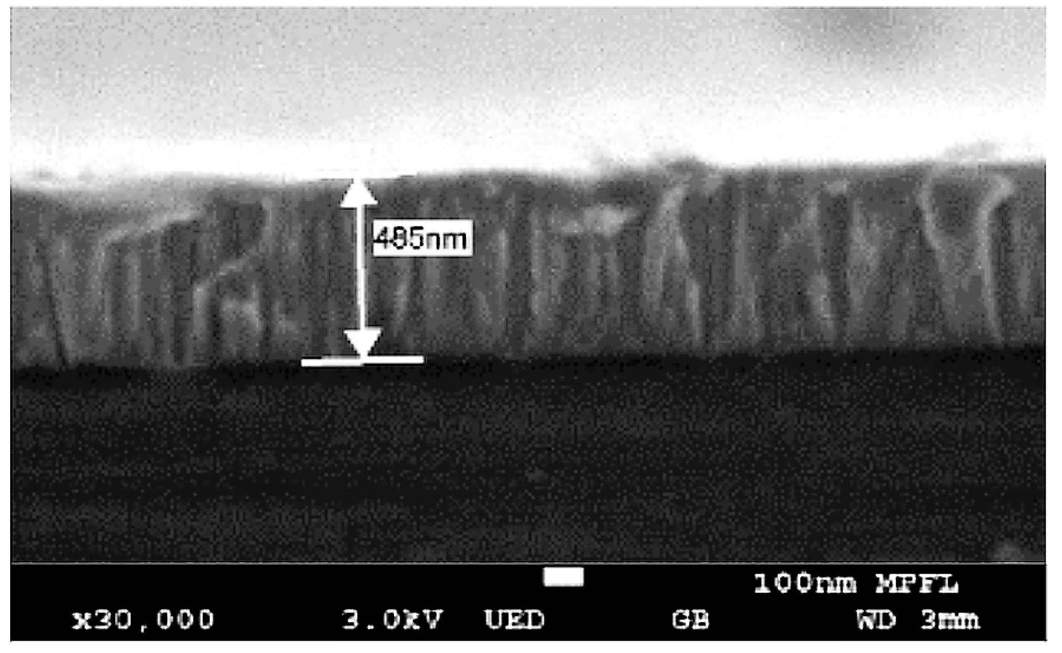
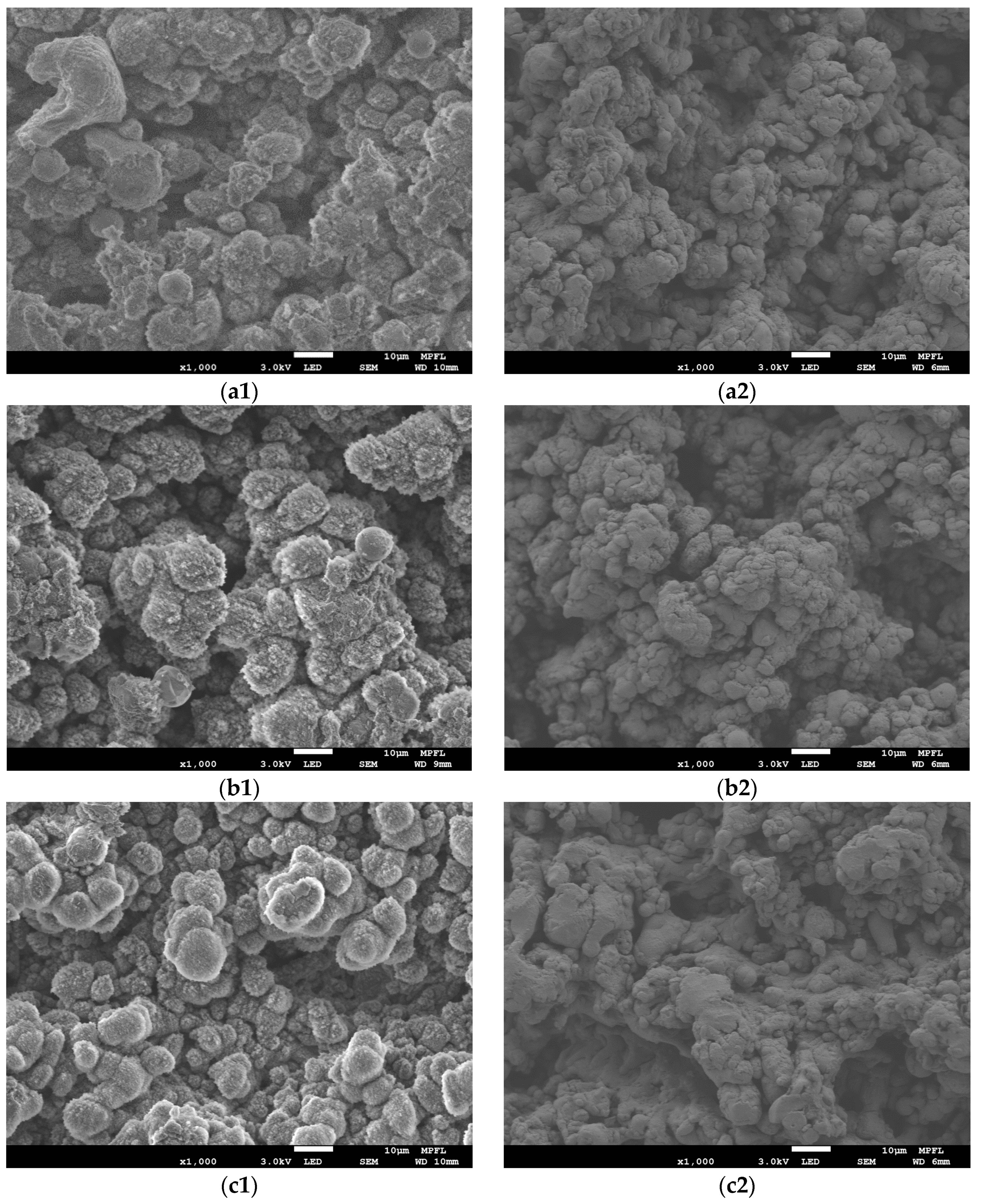
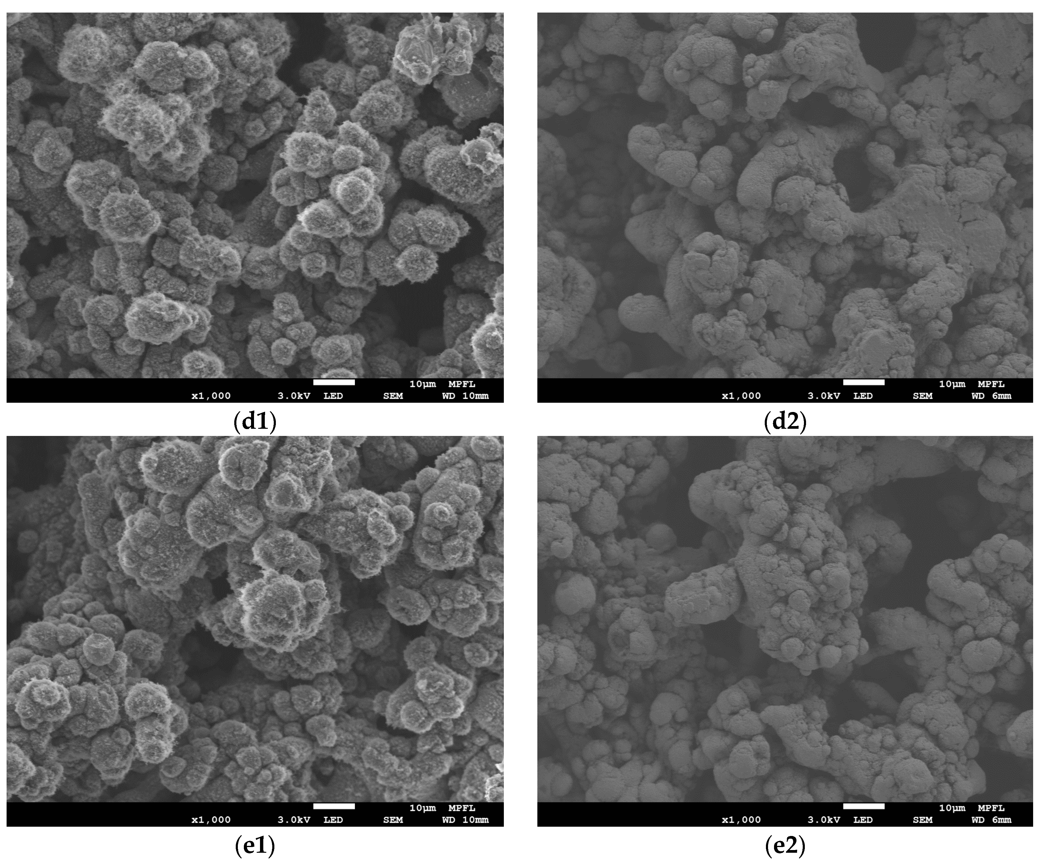
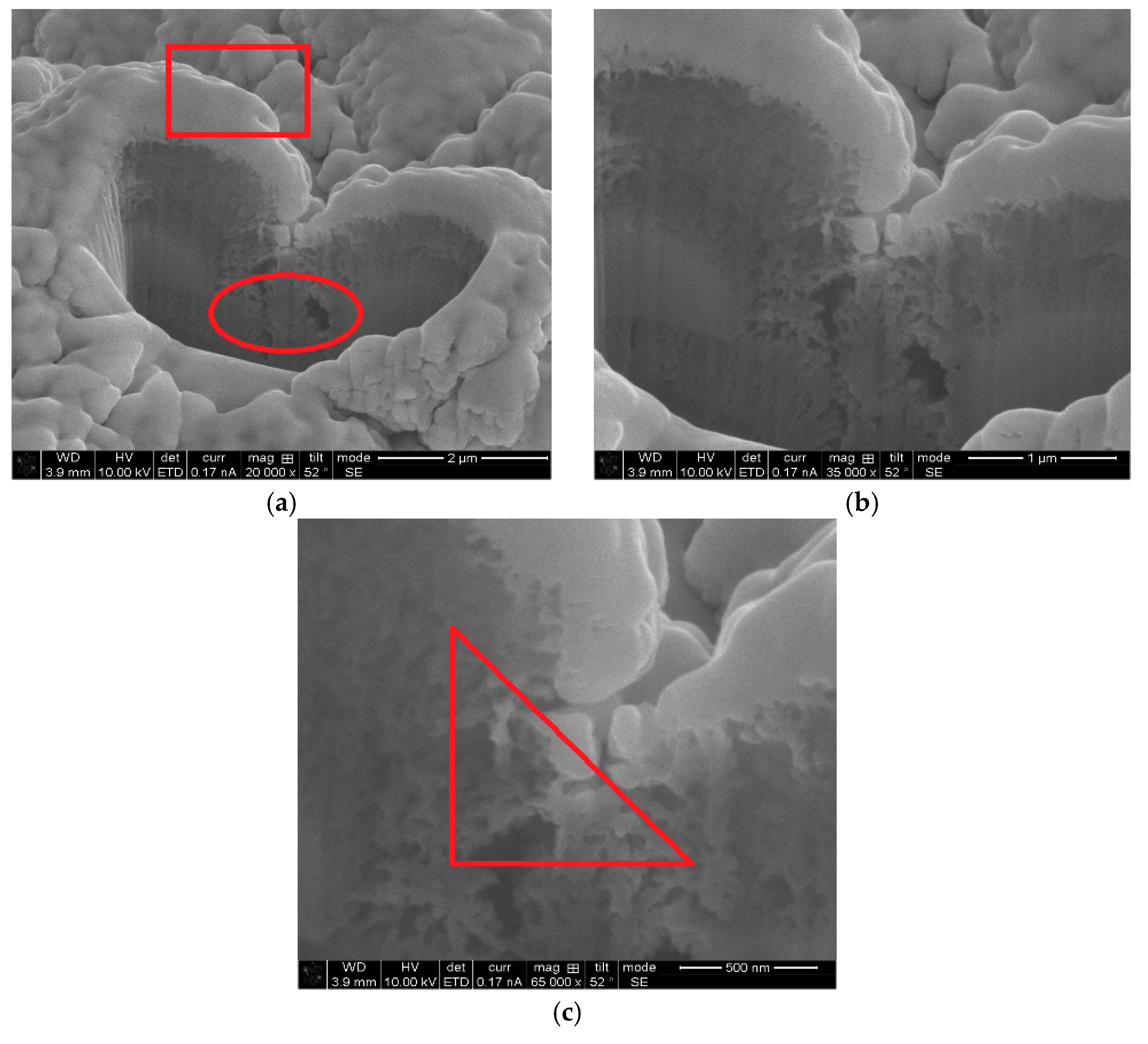
3.1. Surface and Cross-Section Morphology

To assess the thickness of Ti-V-Hf-Zr getter film coatings with laser-treated aluminum alloy substrates, the thickness was measured from the getter film deposited on silicon-substrate taken as a reference. The SEM image of the cross-section of this film is exhibited in Figure 2. It can be seen that the average thickness of the Ti-V-Hf-Zr getter film was about 485 nm.
The surface morphologies of the five laser-treated samples #1–#5 before and after film deposition were investigated by SEM as shown in Figure 3. The grooved surface was obtained after film deposition. The surface morphology of coated laser-treated samples #1–#5 in Figure 3 were much rougher than those of coated untreated aluminum alloy substrate in Figure 4. It can be seen that floccule-like structures were formed on the surface of sphere/columnar-like grains during aluminum surface treatment by laser processing. However, this kind of floccule-like structure was not presented after film deposition. It can be speculated that these nano-size floccule-like structures and profiles with different depth-to-width ratios and angles could influence the SEY properties. Given the surface roughness testing results obtained by LSCM, the influence of surface roughness on the SEY will be discussed in Section 3.3.
FIB-SEM was used to understand the interface between Ti-V-Hf-Zr getter film and the laser-treated substrate surface. The SEM top view images of sample #2 after film deposition are given in Figure 5. The film region is light grey and the aluminum alloy substrate is represented as darker grey. The regions in red rectangle and ellipse of sample #2 in Figure 5a are the Ti-V-Hf-Zr thin film and porous structure after laser engineering, respectively. The aforementioned images clearly show the film and laser-treated aluminum alloy substrates. Figure 5b illustrates that the film thickness of sample #2 on the peak region of the laser-treated surface was higher than that in the valley region. As shown in Figure 5c, the region in the triangle indicates that the Ti-V-Hf-Zr getter film was deposited in the porous surface of the laser-treated substrates where the sputtering metal atoms could reach during the depositing process. By comparing this with the fracture surface morphology of film coatings on silicon substrates in Figure 2, that of the coated laser-treated surface of sample #2 was more rugged in Figure 5. This indicates that the SEY of coated laser-treated sample may be lower than that of coated silicon samples.

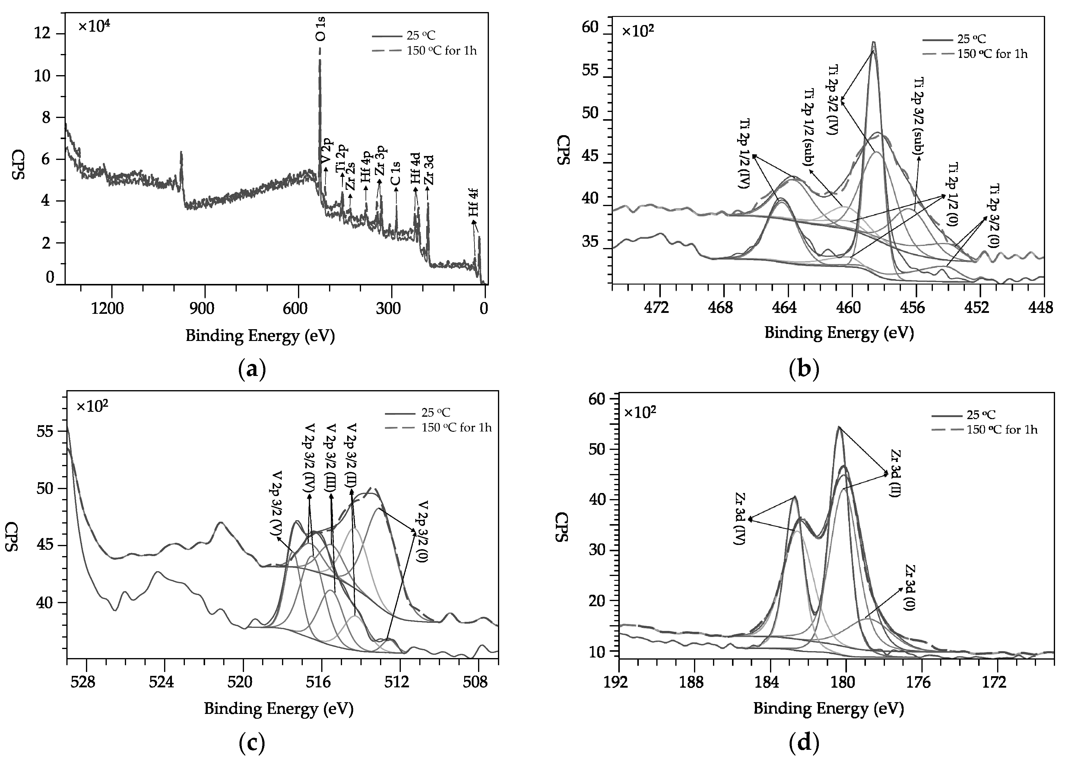
3.2. Surface Composition

Surface chemical state is one of the essential factors affecting the SEYs of films. To realize the surface chemical information, XPS measurements were taken.
The XPS chemistry of the Ti-V-Hf-Zr getter film on laser-treated substrate sample #1 before and after the activation (labelled “150 °C” for 1 h in Figure 6) was studied. Figure 6a shows the survey scan of the activated and unactivated Ti-V-Hf-Zr coated laser-treated sample #1.
As shown in Figure 6b, the Ti 2p3/2 peak of unactivated Ti-V-Hf-Zr coated laser-treated sample #1 exhibits the metallic titanium state at the binding energy (BE) of 454.3 eV (2p3/2) and the oxide structures at the BE of 458.3 eV (2p3/2) [18,19,20]. After the activation, the suboxide titanium appeared at the BE of 456.2 eV (2p3/2). The concentration of titanium oxide decreased about 37.65% after activation.
The V 2p3/2 spectra of Ti-V-Hf-Zr getter film display several elementary peaks which can be seen from the V (V) state at a BE peak of 517.5 eV to metallic vanadium state at a BE of 512.5 eV [21] in Figure 6c. After the activation, the percentage of V 2p(V) decreased dramatically and that of metallic vanadium increased significantly.
In Figure 6d, the Zr 3d spin-orbit doublet peaks for unactivated Ti-V-Hf-Zr getter film were at 182.7 and 180.4 eV for Zr 3d of Zr(IV) state and Zr 3d of Zr(II) state, respectively [22,23]. The fit results of the Zr 3d spectrum after the activation indicate the appearance of metallic Zr. The position of the peak of metallic Zr at 178.8 eV is consistent with the metallic state in reference [24,25].
Figure 6e shows the fit results of the three contributions (Hf metal, Hf suboxide and Hf oxide) for unactivated and activated Ti-V-Hf-Zr getter film on the laser-treated substrate. The spectrum of unactivated Ti-V-Hf-Zr getter film presents three doublets corresponding to various oxidation states: suboxide (4f7/2 at 16.2 eV) and Hf oxide (4f7/2 at 17.0 eV) [26,27]. The ratio of metallic Hafnium (4f7/2 at 14.5 eV) of the activated Ti-V-Hf-Zr getter film was observably higher than that of the unactivated one. The Hf oxide content of Ti-V-Hf-Zr getter film decreased dramatically about 52.5% after the activation.
Therefore, the XPS spectra in Figure 6 demonstrate that the Ti-V-Hf-Zr coated laser-treated aluminum alloy could be partially activated after being heated at 100 and 150 °C, respectively, for 1 h in a vacuum and also used as a pump.
Since it is known that NEG activation temperatures strongly depend on stoichiometry, the average atomic ratios of Ti, V, Hf and Zr elements of the film before and after activation at 100 °C for 1 h and 150 °C for 1 h were around 0.86:1.00:1.13:0.30 and 0.81:1.00:1.12:0.27, respectively, as shown in Figure 6a. On the whole, this variation is basically homogeneous (with element ratio difference of 1%–10%) on the laser-treated sample, probably suggesting that it may imply effective pumping and the NEG activation temperature will be mostly stable for Ti-V-Hf-Zr getter on laser processed aluminum alloy.
In order to investigate the internal stoichiometry of the Ti-V-Hf-Zr getter film, the film surface was bombarded by Ar+ ions. After ion stripping, the internal stoichiometry of the film can be obtained. The average atomic ratios of Ti, V, Hf and Zr elements of the film on sample #1 before and after ion stripping were nearly 1.2:1.0:1.3:1.8 and 1.5:1.0:1.9:1.4, respectively, as shown in Figure 6f. The elements ratios of the Ti and Hf elements of the stripped one increased about 20% and 31%, respectively, and that of Zr element decreases about 29%, compared with that of the unstripped Ti-V-Hf-Zr getter film. It can be speculated that the Ti-V-Hf-Zr getter film grows non-stoichiometrically on deep lying holes in the nanostructure. Moreover, the average element ratio of the target was 1:1:1:1. While the film elements ratios is different with that of the target. The elements ratio difference is caused by different sputtering yields of different metal elements and the interaction between various atoms.

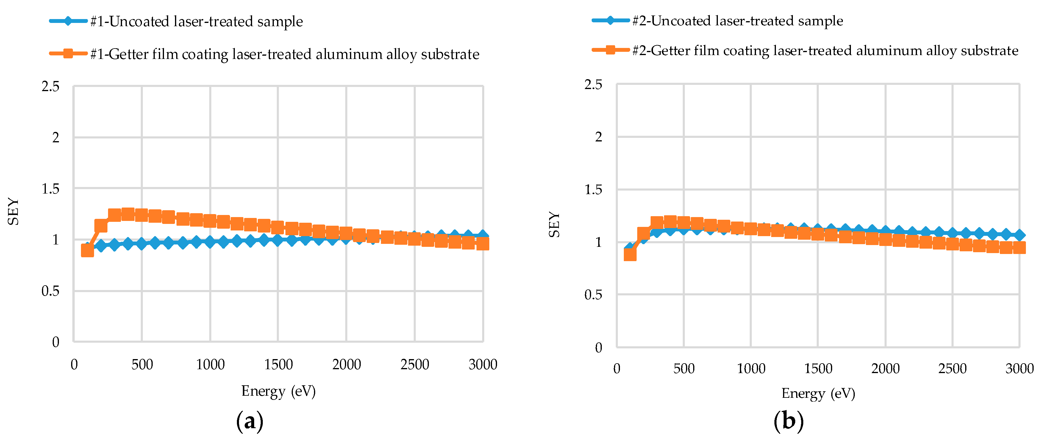
3.3. Secondary Electron Yield (SEY) Results

The SEY results of coated and uncoated laser-treated aluminum alloy substrates are plotted in Figure 7a–e, with the primary energy (Ep) ranging from 100 to 3000 eV. The SEYs of unactivated NEG films on Sample #1–#5 were examined.
The blue SEY curve of laser-treated sample #1 continues to rise at 100 ≤ Ep ≤ 3000 eV, as shown in Figure 7a. In the meantime, the blue SEY curve of laser-treated sample #2 increases linearly at 100 ≤ Ep ≤ 500 eV and then decreases gradually. The δmax of treated sample #1 and of sample #2 after getter film deposition were 1.25 and 1.19, respectively, as depicted in Figure 7a,b. The shapes of orange SEY curves of the NEG coated laser-treated sample #1 and of sample #2 are very similar. Furthermore, the corresponding primary energy (Emax) of δmax were 400 eV for both samples. The surface roughnesses of these two samples were close, up to 8.654 and 8.763 μm, respectively, which may contribute the similar curve shapes.
In Figure 7b,c, at Ep ≤ 500 eV, the maximum SEYs of uncoated laser-treated sample #2 (blue curves) with a scanning speed of 100 mm·s−1 and uncoated laser-treated sample #3 (blue curves) of 150 mm·s−1 were 1.12 and 1.00, respectively. Nevertheless, after getter film deposition, the maximum SEYs of the getter coated samples #2 and #3 (orange curves) were 1.19 and 1.34 at Ep ≤ 500 eV, respectively. As a result, the scanning speed could influence the SEY of laser-treated aluminum alloy samples before and after film deposition, thereby leading to various maximum SEY variation trends. In Figure 7d,e, both with the same non-equidistant laser-processing pattern, the δmax of uncoated laser-treated sample #4 (blue curve) with the scanning speed of 100 mm·s−1 and the uncoated laser-treated sample #5 (blue curve) of 150 mm·s−1 were 1.26 and 1.10, respectively. However, the δmax of getter coated sample #4 and #5 (orange curves) after film deposition were 1.06 and 1.48, respectively.
As presented in Figure 7a–e, the value of the SEY after coating might be higher and lower than that of the respective sample without coating. Several factors, such as surface roughness, topography etc., can influence the SEY results of the samples. The surface roughnesses of the getter film coated laser-treated aluminum alloy samples decreased by about 5.5%–22.0%, compared with that of uncoated ones.
In Figure 7f, the blue curve indicates the SEY of uncoated untreated aluminum alloy and the orange one represents that of the NEG coated untreated aluminum alloy. By comparing with the blue curve of uncoated and untreated aluminum alloy sample in Figure 7f, it can be seen that the maximum SEY of the blue curve in Figure 7a of uncoated laser-treated sample #1 with a pitch spacing of 15 µm and that of the blue curve in Figure 7b of uncoated laser-treated sample #2 with a pitch spacing of 20 µm decreased from 2.30 to 1.04 and 1.13, respectively. The δmax of as-received bare aluminum alloy reported by several other researchers from Science and Technology Facilities Council (STFC) Daresbury Laboratory, National Institute for Nuclear Physics (INFN), German Electron Synchrotron (DESY) and European Organization for Nuclear Research (CERN) varied between 2.55 and 3.50 [10,28,29,30]. The δmax difference of the untreated aluminum alloy might be related to the surface morphology and the oxide thickness of the surface.
As shown in Figure 7, the δmax of uncoated laser-treated aluminum alloy were lower than that of untreated bare aluminum alloy, and such yield value difference is primarily caused by the induced surface geometrical modification. After film deposition, the δmax of coated untreated aluminum alloy was lower than that of uncoated untreated aluminum alloy. The variations of surface morphologies (Figure 4) and chemical components changes both could contribute to the SEY reduction. However, the δmax of the getter coated laser-treated aluminum alloy is sometimes lower or higher than that of the uncoated laser-treated aluminum alloy. The reasons for the SEY change trend difference of coated and uncoated laser-treated aluminum alloy are complicated. Several factors, such as surface morphology, surface chemical states etc., may contribute to this difference.
The Emax of SEY curves of laser-treated aluminum alloy varied between 700 and 3000 eV at 100 ≤ Ep ≤ 3000 eV in this study. After Ti-V-Hf-Zr getter film deposition, the Emax of SEY curves of coated laser-treated aluminum alloy ranged from 300 to 500 eV. It is worth noting that the Emax decreased dramatically after film deposition. This may be ascribed to the surface chemical states (such as the elements and the oxidation states) and the variations of surface morphologies before and after Ti-V-Hf-Zr getter film deposition. Firstly, the surface elements were totally different for Ti-V-Hf-Zr coated and uncoated laser-treated aluminum alloy samples. Secondly, a passivation layer was formed on the Ti-V-Hf-Zr getter surface before the SEY measurements, due to the exposure to the air during sample transfer. Thirdly, the roughnesses of the coated samples were lower than the uncoated laser-treated ones, as shown in Table 1. A rough surface has generally a high Emax, as reported by Isabel Montero et al. [31,32]. Thus, these three aspects may be associated with the Emax decrease of the coated ones.
It can be seen that the SEY curves of the getters manifests in an asymmetric peak shape evolution and those of the uncoated laser-treated aluminum alloy surface manifests in a monotone increase with increasing PE. It is demonstrated that SEY has an asymmetric peak for a smooth metallic surface and in a monotonic increase curve on a rough metallic surface [33,34]. The same SEY trend tendency was verified for the dielectric materials but with a higher amplitude intensity (because of scattering related to the high resistivity effect in dielectrics) [33]. On the whole, the SEY curves mainly depend on material, surface roughness, incident electron parameters, etc. [33,34,35,36]. In this study, these five samples were treated by laser with two different hatched patterns (equidistant and non-equidistant patterns), different scanning speeds and different pitch spacings. These three factors (laser-hatched patterns, scanning speeds and pitch spacings), can contribute to the surface roughness difference. By comparing the measured SEY curves, one can deduce the effect of the roughness on the SEY behavior and, consequently, predict which laser-treated substrate surface characteristics would have a remarkable effect on the getter SEY properties.
Compared with the δmax of Ti-Zr-V getter film which has been widely used in many accelerators, such as Large Hadron Collider (LHC) [37,38], the High Energy Accelerator Research Organization (KEK) B-Factory [39] etc., that of as-received Ti-Zr-V getter film with aluminum alloy substrates was about 2.10 with the δmax at 300 eV [40]. This indicates that the Emax of Ti-V-Hf-Zr getter film is lower than that of Ti-Zr-V film with aluminum alloy substrates. According to reference [41], the δmax of TiN thin films with aluminum alloy substrates were 1.5~2.4. The δmax of amorphous carbon films were 0.9–1.3 [42]. For TiZr binary metal alloy films, the δmax varied between 1.0 and 2.1 under different activation conditions [43]. The δmax of Ti-V-Hf-Zr getter film on laser-treated aluminum alloy substrate was found to be close to that of amorphous carbon films, and lower than that of TiN thin films and as-received TiZr binary metal alloy films.
The application of the Ti-V-Hf-Zr coated and uncoated laser-treated aluminum alloy in future accelerators is mostly questioned not by the SEY but mainly by the potentially detrimental effect on the machine impedance budget. Compared to the pumping capability of uncoated laser-treated aluminum alloy, that of Ti-V-Hf-Zr coated one can be more higher. Moreover, the SEYs of Ti-V-Hf-Zr coated and uncoated laser-treated aluminum alloy can both be close to 1, which can be effective for electron cloud mitigation.

4. Conclusions

For the purpose of improving the vacuum and mitigating the electron clouds in ultra-high vacuum chamber systems, the combination of NEG films and laser structuring patterns on a substrate surface was proposed in this work.
Firstly, the SEM results indicate that floccule-like structures were formed on the surface of sphere/columnar-like grains after the laser-structuring process, and not presented on the NEG film-coated laser-treated substrates. FIB-SEM results manifest that the film thickness on the peak region of the laser-treated surface was higher than that in the valley region.
Secondly, the XPS analysis results show the decreases of titanium oxide, vanadium oxide, zirconium oxide and hafnium oxide concentrations and the increases of metallic titanium, vanadium, zirconium and hafnium concentrations. Thus, the Ti-V-Hf-Zr getter film-coated laser-treated aluminum alloy could be partially activated after heating at 100 and 150 °C, respectively, for 1 h in vacuum and could also act as a pump.
Thirdly, the SEYs of coated Ti-V-Hf-Zr getter film with laser-treated surfaces can be higher or lower than the uncoated laser-treated ones at 100 ≤ Ep ≤ 3000 eV. Several factors, such as surface morphology, surface chemical states etc., may contribute to this SEY difference. The δmax of Ti-V-Hf-Zr getter film coating laser-treated aluminium alloy substrates can be reduced to ~1.1. The δmax of activated Ti-V-Hf-Zr getter films might be lower than 1. It can be speculated that Ti-V-Hf-Zr getter film coating laser-treated aluminium alloy substrates can be considered as a promising candidate for electron mitigation.
Finally, the application of the Ti-V-Hf-Zr coated and uncoated laser-treated aluminum alloy in future accelerators is also questioned by the potentially detrimental effect on the machine impedance budget. Thus, the possibility that such a surface loses particles during operation is a crucial issue for particle accelerators which requires rigorous evaluation in the future.

Author Contributions

Conceptualization, J.W.; Data curation, J.W., Y.G., Z.Y., J.F. and J.Z.; Formal analysis, Z.X.; Funding acquisition, S.W. and Z.X.; Investigation, J.W., Y.G. and Z.Q.; Methodology, Z.Y., J.F., J.Z. and Z.Q.; Supervision, S.W. and Z.X.; Validation, J.W. and Y.G.; Writing—original draft, J.W.; Writing—review and editing, J.W., S.W. and Z.X.

Funding

This work was supported by the key project of Intergovernmental International Scientific and Technological Innovation Cooperation in China under Grant No. 2016YFE0128900, China Postdoctoral Science Foundation Grant No. 2018M643667, the National Natural Science Foundation for the Youth of China No. 11905170, the Fundamental Research Funds for the Central Universities No. XJH012019018, Shaanxi Province Postdoctoral Science Foundation Grant No. 2018104, the Fundamental Research Funds for the Central Universities No. XJH012019011 and the National Natural Science Foundation of China under Grant No. 11775166.

Acknowledgments

We thank Shengli Wu and Jie Li from Institute of Physical Electronics and Devices of Xi’an Jiaotong University for help with SEY tests.

Conflicts of Interest

The authors declare no conflict of interest.

References

  1. Malyshev, O.B.; Valizadeh, R.; Jones, R.M.A.; Hannah, A. Effect of coating morphology on the electron stimulated desorption from Ti-Zr-Hf-V nonevaporable-getter-coated stainless steel. Vacuum 2012, 86, 2035–2039. [Google Scholar] [CrossRef]
  2. Malyshev, O.B.; Valizadeh, R.; Hannah, A. Pumping properties of Ti-Zr-Hf-V non-evaporable getter coating. Vacuum 2014, 100, 26–28. [Google Scholar] [CrossRef]
  3. Malyshev, O.B.; Valizadeh, R.; Hannah, A. Pumping and electron-stimulated desorption properties of a dual-layer nonevaporable getter. J. Vac. Sci. Technol. A 2016, 34, 061602. [Google Scholar] [CrossRef] [Green Version]
  4. Amador, L.L.; Chiggiato, P.; Ferreira, L.M.A.; Nistor, V.; Fontenla, A.T.P.; Taborelli, M.; Vollenberg, W.; Doche, M.L.; Hihn, J.Y. Development of copper electroformed vacuum chambers with integrated nonevaporable getter thin film coatings. J. Vac. Sci. Technol. A 2018, 36, 021601. [Google Scholar] [CrossRef]
  5. Benvenuti, C.; Cazeneuve, J.M.; Chiggiato, P.; Cicoira, F.; Santana, A.E.; Johanek, V.; Ruzinov, V.; Fraxedas, J. A novel route to extreme vacua: The non-evaporable getter thin film coatings. Vacuum 1999, 53, 219–225. [Google Scholar] [CrossRef]
  6. Lozano, M.P.; Fraxedas, J. XPS analysis of the activation process in non-evaporable getter thin films. Surf. Interface Anal. 1999, 30, 623–627. [Google Scholar] [CrossRef]
  7. Porcelli, T.; Puro, M.; Raimondi, S.; Siviero, F.; Maccallini, E.; Manini, P.; Bongiorno, G. NEG coating deposition and characterisation of narrow-gap insertion devices and small-diameter chambers for light sources and particle accelerators. Vacuum 1999, 138, 157–164. [Google Scholar] [CrossRef]
  8. Yusuke, S.; Kyo, S.; Takuya, I.; Hitoshi, F.; Makoto, T.; John, F.; Emy, M.; Mitsuru, S.; Shinji, T.; Ken-ichi, K.; et al. Achievements and problems in the first commissioning of superKEKB vacuum system. J. Vac. Sci. Technol. A 2017, 35, 03E103. [Google Scholar]
  9. Rumolo, G.; Bartosik, H.; Belli, E.; Dijkstal, P.; Iadarola, G.; Li, K.; Mether, L.; Romano, A.; Schenk, M.; Zimmermann, F. Electron cloud effects at the LHC and LHC injectors. In Proceedings of the IPAC 2017, Copenhagen, Denmark, 14–19 May 2017. [Google Scholar]
  10. Valizadeh, R.; Malyshev, O.B.; Wang, S.; Sian, T.; Cropper, M.D.; Sykes, N. Reduction of secondary electron yield for E-cloud mitigation by laser ablation surface engineering. Appl. Surf. Sci. 2017, 404, 370–379. [Google Scholar] [CrossRef] [Green Version]
  11. Wang, J.; Xu, Y.; Zhang, B.; Wei, W.; Fan, L.; Pei, X.; Hong, Y.; Wang, Y. Experimental study on TiN coated racetrack-type ceramic pipe. Chin. Phys. C 2017, 39, 117005. [Google Scholar] [CrossRef]
  12. Lee, K.; Kim, W.G.; Cho, J.Y.; Eun, S.W.; Choe, H.C. Effects of TiN film coating on electrochemical behaviours of nanotube formed Ti-xHf alloys. Trans. Nonferrous Met. Soc. China 2009, 19, 857–861. [Google Scholar] [CrossRef]
  13. Vallgren, Y.; Arduini, G.; Bauche, J.; Calatroni, S.; Chiggiato, P.; Cornelis, K.; Pinto, P.C.; Henrist, B.; Métral, E.; Neupert, H.; et al. Amorphous carbon coatings for the mitigation of electron cloud in the CERN Super Proton Synchrotron. Phys. Rev. Spec. Top. Accel. Beams 2011, 14, 071001. [Google Scholar] [CrossRef]
  14. Vallgren, C.Y.; Chiggiato, P.; Pinto, P.C.; Neupert, H.; Rumolo, G.; Shaposhnikova, E.; Taborelli, M.; Kato, S. Performance of carbon coatings for mitigation of electron cloud in the SPS. In Proceedings of the IPAC 2011, San Sebastián, Spain, 4–9 September 2011. [Google Scholar]
  15. Eldred, J.; Backfish, M.; Tan, C.Y.; Zwaska, R.; Kato, S. Beam tests of diamond-like carbon coating for mitigation of electron cloud. In Proceedings of the IPAC 2017, Copenhagen, Denmark, 14–19 May 2017. [Google Scholar]
  16. Wang, J.; Wang, Y.; Xu, Y.; Zhang, Y.; Zhang, B.; Wei, W. Secondary electron emission characteristics of graphene films with copper substrate. Chin. Phys. C 2016, 40, 117003. [Google Scholar] [CrossRef]
  17. Wang, J.; Gao, Y.; Fan, J.; You, Z.; Wang, S.; Xu, Z. Study on the effect of laser parameters on the SEY of aluminum alloy. IEEE Trans. Nucl. Sci. 2019, 66, 609–615. [Google Scholar] [CrossRef]
  18. Atuchin, V.V.; Kesler, V.G.; Pervukhina, N.V.; Zhang, Z. Ti 2p and O 1s core levels and chemical bonding in titanium-bearing oxides. J. Electron Spectrosc. 2006, 152, 18–24. [Google Scholar] [CrossRef]
  19. Hashimoto, S.; Murata, A.; Sakurada, T.; Tanaka, A. Change of Ti 2p XPS spectrum for titanium oxide by Ar ion bombardment. J. Surf. Anal. 2003, 10, 12–15. [Google Scholar]
  20. Šutara, F.; Tsud, N.; Veltruská, K.; Matolín, V. XPS and ESD study of carbon and oxygen chemistry on TiZrV NEG. Vacuum 2001, 61, 135–139. [Google Scholar] [CrossRef]
  21. Matolin, V.; Masek, K.; Matolinova, I.; Skala, T.; Veltruska, K. XPS and SIMS study of the ageing mechanism of Zr-V non-evaporable getter films. Appl. Surf. Sci. 2004, 235, 202–206. [Google Scholar] [CrossRef]
  22. Barreca, D.; Battiston, G.A.; Gerbasi, R.; Tondello, E.; Zanella, P. Zirconium dioxide thin films characterized by XPS. Surf. Sci. Spectra 2000, 7, 303–309. [Google Scholar] [CrossRef]
  23. Matolin, V.; Drbohlav, J.; Masek, K. Mechanism of non-evaporable getter activation XPS and static SIMS study of Zr44V56 alloy. Vacuum 2003, 71, 317–322. [Google Scholar] [CrossRef]
  24. Sharma, S.K.; Strunskus, T.; Ladebusch, H.; Zaporojtchenko, V.; Faupel, F. XPS study of the initial oxidation of the bulk metallic glass Zr46.75Ti8.25Cu7.5Ni10Be27.5. J. Mater. Sci. 2008, 43, 5495–5503. [Google Scholar] [CrossRef]
  25. Sharma, S.K.; Strunskus, T.; Ladebusch, H.; Faupel, F. Surface oxidation of amorphous Zr65Cu17.5Ni10Al7.5 and Zr46.75Ti8.25Cu7.5Ni10Be27.5. Mater. Sci. Eng. A 2001, 304–306, 747–752. [Google Scholar] [CrossRef]
  26. Engelhard, M.; Herman, J.; Wallace, R.; Baer, D. As-received, ozone cleaned and Ar+ sputtered surfaces of hafnium oxide grown by atomic layer deposition and studied by XPS. Surf. Sci. Spectra 2011, 18, 46–57. [Google Scholar] [CrossRef]
  27. Barreca, D.; Milanov, A.; Fischer, R.A.; Devi, A.; Tondello, E. Hafnium oxide thin film grown by ALD: An XPS study. Surf. Sci. Spectra 2007, 14, 34–40. [Google Scholar] [CrossRef]
  28. Baglin, V.; Bojko, J.; Gröbner, O.; Henrist, B.; Hilleret, N.; Scheuerlein, C.; Taborelli, M. The secondary electron yield of technical materials and its variation with surface treatments. LHC Proj. Rep. 2000, 433, 1–5. [Google Scholar]
  29. Grosso, D.R.; Commisso, M.; Cimino, R.; Flammini, R.; Larciprete, R.; Wanzenberg, R. SEY of Al samples from the dipole chamber of PETRA III at DESY. In Proceedings of the IPAC 2011, San Sebastián, Spain, 4–9 September 2011; pp. 1533–1535. [Google Scholar]
  30. Grosso, D.R.; Commisso, M.; Cimino, R.; Larciprete, R.; Flammini, R.; Wanzenberg, R. Effect of the surface processing on the secondary electron yield of Al alloy samples. Phys. Rev. Spec. Top AC 2013, 16, 051003. [Google Scholar] [CrossRef] [Green Version]
  31. Pinto, P.C.; Calatroni, S.; Neupert, H.; Letant-Delrieux, D.; Edwards, P.; Chiggiato, P.; Taborelli, M.; Vollenberg, W.; Yin-Vallgren, C.; Colaux, J.L.; et al. Carbon coatings with low secondary electron yield. Vacuum 2013, 98, 29–36. [Google Scholar] [CrossRef] [Green Version]
  32. Montero, I.; Aguilera, L.; Dávila, M.E.; Nistor, V.C.; González, L.A.; Galán, L.; Raboso, D.; Ferritto, R. Secondary electron emission under electron bombardment from graphene nanoplatelets. Appl. Surf. Sci. 2014, 291, 74–77. [Google Scholar] [CrossRef]
  33. Balcon, N.; Payan, D.; Belhaj, M.; Tondu, T.; Inguimbert, V. Secondary electron emission on space materials: Evaluation of the total secondary electron yield from surface potential measurements. IEEE Trans. Plasma Sci. 2012, 40, 282–290. [Google Scholar] [CrossRef]
  34. Thomas, S.; Pattinson, E.B. The controlled preparation of low SEE surfaces by evaporation of metal films under high residual gas pressures. J. Phys. D Appl. Phys. 1970, 3, 1469. [Google Scholar] [CrossRef]
  35. Bojko, I.; Hilleret, N.; Scheuerlein, C. Influence of air exposures and thermal treatments on the secondary electron yield of copper. J. Vac. Sci. Technol. A 2000, 18, 972–979. [Google Scholar] [CrossRef] [Green Version]
  36. James, M.S.; Ronald, A.C.; Robert, A.L., Jr.; Tod, L. Engineered surfaces to control secondary electron emission for multipactor suppression. In Proceedings of the 2016 IEEE National Aerospace and Electronics Conference (NAECON) and Ohio Innovation Summit (OIS), Dayton, OH, USA, 25–29 July 2016; pp. 296–302. [Google Scholar]
  37. Kamiya, J.; Baglin, V.; Bregliozzi, G.; Jimenez, J.M. Outgassing measurement of an LHC collimator and estimation for the NEG performances. Vacuum 2011, 85, 1178–1181. [Google Scholar] [CrossRef]
  38. Mahner, E.; Hansen, J.; Küchler, D.; Malabaila, M.; Taborelli, M. Ion-stimulated gas desorption yields of electropolished, chemically etched, and coated (Au, Ag, Pd, TiZrV) stainless steel vacuum chambers and St707 getter strips irradiated with 4.2 MeV/u lead ions. Phys. Rev. Spec. Top AC 2005, 8, 053201. [Google Scholar] [CrossRef] [Green Version]
  39. Suetsugu, Y.; Kanazawa, K.; Shibata, K.; Hisamatsu, H.; Oide, K.; Takasaki, F.; Dostovalov, R.V.; Krasnov, A.A.; Zolotarev, K.V.; Konstantinov, E.S.; et al. First experimental and simulation study on the secondary electron and photoelectron yield of NEG materials (Ti-Zr-V) coating under intense photon irradiation. Nucl. Instrum. Meth. A 2005, 554, 92–113. [Google Scholar] [CrossRef]
  40. Pimpec, L.; King, F.; Kirby, R.E.; Pivi, M.; Rumolo, G. The Continuing Story of Secondary Electron Yield Measurements from TiN Coating and TiZrV Getter Film. SLAC-TN-04-046\LCC-0146; Stanford Linear Accelerator Center: Menlo Park, CA, USA, 2004. [Google Scholar]
  41. Pimpec, L.; Kirby, R.E.; King, F.; Pivi, M. Properties of TiN and TiZrV thin film as a remedy against electron cloud. Nucl. Instrum. Meth. A 2005, 551, 187–199. [Google Scholar] [CrossRef]
  42. Vallgren, C.Y.; Arduini, G.; Bauche, J.; Calatroni, S.; Chiggiato, P.; Cornelis, K.; Pinto, P.C.; M’etral, E.; Rumolo, G.; Shaposhnikova, E.; et al. Amorphous carbon coatings for mitigation of electron cloud in the CERN SPS. In Proceedings of the IPAC’10, Kyoto, Japan, 23–28 May 2010; pp. 2033–2035. [Google Scholar]
  43. Henrist, B.; Hilleret, N.; Scheuerlein, C.; Taborelli, M. The secondary electron yield of TiZr and TiZrV non-evaporable getter thin film coatings. Appl. Surf. Sci. 2001, 172, 95–102. [Google Scholar] [CrossRef] [Green Version]
Figure 1. Laser-hatched patterns for laser-treated aluminum alloy substrates at repetition rate of 20 kHz and scanning speed of 100 mm·s−1. (a) equidistant pattern; (b) non-equidistant pattern.
Coatings 09 00839 g001
Figure 2. The cross-section scanning electron microscope (SEM) images of Ti-V-Hf-Zr getter film deposited on silicon substrate.
Coatings 09 00839 g002
Figure 3. SEM images of Ti-V-Hf-Zr getter film coatings and aluminum alloy substrates which were treated by different laser parameters. Those on the left are the surface morphologies of laser-treated aluminum alloy sample #1–#5: (a1) sample #1; (b1) sample #2; (c1) sample #3; (d1) sample #4; (e1) sample #5, and those on the right are the surface morphologies of Ti-V-Hf-Zr getter film coatings with cleaned laser-treated aluminum alloy substrates: (a2) sample #1; (b2) sample #2; (c2) sample #3; (d2) sample #4; (e2) sample #5.
Coatings 09 00839 g003aCoatings 09 00839 g003b
Figure 4. SEM images of (a) untreated aluminum alloy and (b) Ti-V-Hf-Zr getter film-coated cleaned aluminum alloy substrate.
Coatings 09 00839 g004
Figure 5. Selection of the regions of interest within Ti-V-Hf-Zr getter film coatings sample #2 for serial focused ion beam (FIB)-SEM top view images at different scales (a) 2 μm, (b) 1 μm and (c) 500 nm.
Coatings 09 00839 g005
Figure 6. X-ray photoelectron spectroscopy (XPS) spectra of unactivated and activated Ti-V-Hf-Zr getter film coatings with laser-treated substate sample #1: (a) survey scan; (b) Ti 2p; (c) V 2p; (d) Zr 3d and (e) Hf 4f. (f): survey scan of stripped and unstripped getter film.
Coatings 09 00839 g006aCoatings 09 00839 g006b
Figure 7. Secondary electron yield (SEY) results of Ti-V-Hf-Zr getter film coated and uncoated laser-treated aluminum alloy: (a) sample #1, (b) sample #2, (c) sample #3, (d) sample #4 and (e) sample #5. (f) The SEY results of untreated aluminum alloy and Ti-V-Hf-Zr getter film coated untreated aluminum alloy. Sample #1, #2 and #3 were treated by laser under equidistant pattern and sample #4 and #5 with non-equidistant pattern. The SEY curves of the films on sample #1–#5 are unactivated here.
Coatings 09 00839 g007aCoatings 09 00839 g007b
Table 1. Laser parameters used for processing the aluminum alloy substrates.
SampleHatched PatternsPitch Spacing/μmScanning Speed/mm·s−1Laser-TreatedAfter Film Deposition
δmaxEmax/eVRa/μmδmaxEmax/eVRa/μm
#1Figure 1a151001.04300010.31.254008.7
#2Figure 1a201001.137009.11.194008.8
#3Figure 1a201501.0424007.41.343005.8
#4Figure 1b5–251001.25300010.41.065009.9
#5Figure 1b5–251501.10300014.81.4830013.5

