Abstract
Nano-texturing of polymers offers the possibility to drive important surface properties such as wettability and anti-reflectivity. Interestingly, plasma can lead to the desired characteristic of nanofeatures through a one step process based onto dry plasma etching. In this work, the literature concerning such plasma nano-texturing will be reviewed for different polymers, and in particular, for applications based upon wettability control. Then the mechanism of such processes will be commented upon, with a glance to the different characteristics of the polymers. Finally, some hints onto a feasible approach to plasma nano-texturing of the different polymers will be given.
1. Introduction: Why?
The first question this review wishes to answer is “why could we need plasma nano-texturing?”, and this is mostly related to biomimetics. In biomimetics, technological problems are solved by looking at similar issues in nature (plants or animals), and understanding the biological mechanisms applied by the living organism to overcome such problems. Then the material scientist, inspired by such nature observation, has to shape matter, producing a device with a feasible chemical, physical and morphological structure [1]. Often, living organisms adapt to environment stimuli, playing with texturing in the nanoscale and microscale domain, coupled to a suitable chemical composition [2]. In Table 1, some typical examples of a biological surface with unique characteristics related to wettability properties are reported.

Table 1.
Examples of nano-/micro-textured biological surfaces.
It is well known that nano- and micro-roughness drastically influence the wetting behavior of surfaces. Besides some discussion relative to the appropriateness of the Wenzel and Cassie–Baxter description of the effect of roughness [13,14,15,16], it is commonly believed that: (i) Smooth surfaces cannot exhibit a Water Contact Angle (WCA) higher than 120° (like in the case of Teflon® (Polytetrafluoroethylene (PTFE)) and silicone); (ii) a surface can be considered water repellent for a WCA higher than 150° and a small contact angle hysteresis (typically lower than 10°); (iii) This regime, leading to self cleaning and low water adhesive surfaces, can be obtained only through suitable surface texturing [1]; (iv) last but not least, on a textured surface a critical value of the equilibrium contact angle exists, below which water completely impregnates through the protrusions [17]. In nature, such textured surfaces are often present for a better exploitation of water surface energy-related properties.
The texture of some plant leaves, such as those of lotus, rice and Salvinia have been studied for water repellency and self-cleaning due to the presence of nano- and micro-protuberances, coated with a hydrophobic wax [6,7,12]. Such hydrophobic surface texture is present in some animals for drag reduction. This is the case of shark skin, consisting of micron scales and nano-scale riblet structures [18], or the ability of the water strider to run on water in ponds, thanks to super-hydrophobic-oriented microsetae (microscopic hairs), covered with grooved nanostructures that exist upon the insect legs [11]. On the other hand, the nano-texturing coupled to the superhydrophobic character can be “sticky”, like in rose petals, and in some cases can lead to super-adhesive behavior, as for the Gecko legs [9,10]. The desert beetle, having a nano-textured surface on the body with alternating super-hydrophobic and super-hydrophilic spots, can optimize the condensation of water vapor and collection at the mouth level, and it can overcome the dryness of the environment [8]. Finally, mostly in the animal kingdom, it should be mentioned that insects make an efficient use of texturing to control, not only wettability, but also optical properties, such as light reflection [4] and structural coloration [3].
Hence, mimicking nature, in producing chemically-defined nano- and micro-texturing, can improve the design of smart materials and devices, that can find application in fog collection or resistance, anti-icing, efficient energy conversion, and biological sensors.
This can be achieved by nanofabrication methods. These methods are commonly classified into additive (bottom-up) and subtractive (top-down) manufacturing processes. These processes can sometimes be used in combination to better optimize the final material surface [19,20].
Depending upon the material and the desired feature size, bottom up or top-down methods are used: Typically the former can be less expensive and complex, being that the latter is mostly based upon multi-step photolithography [21].
Bottom-up processes include: Molecular self-assembly [22], vapor deposition (atomic layer, Plasma-enhanced, physical/chemical) [23], the sol-gel method [24], electrospinning [25] and DNA scaffolding [26]. Top-down processes include: E-beam lithography [27], Soft lithography [28], Nanoimprint lithography [29], Block copolymer lithography [30], phase separation [31] and plasma nano-texturing, which itself is the object of this review.
Non-equilibrium plasmas, attracting interest at the early stage of their evolution for producing ultraviolet–visible spectroscopy (UV-Vis) light, found the most outstanding technological application at the beginning of the 1970s for their application in microelectronics. Miniaturized integrated circuits invaded technological commodities, thanks to the introduction of plasma treatment, etching and deposition of material on silicon wafers.
When, in a suitable vacuum reactor, a proper electric field is applied to a gas/vapor mixture at low pressure (typically below 10 Torr) a non-equilibrium cold plasma can be ignited. The electric field accelerates naturally-occurring ions and electrons in the feed, triggering an avalanche of ionization, excitation and bonds breaking reactions, with the formation of active species such as atoms, radicals and molecules in ground and excited levels, Vis-UV photons, as well as new ions and free electrons [32]. Typically, radiofrequency (RF) and microwave (MW) alternating electric fields are used for triggering plasma.
The key of plasma technology is the possibility of tuning the relative abundance of these species in a cold environment (commonly below 60 °C) to drive, basically, three kind of process: Dry etching, plasma deposition and plasma treatment [33].
Dry etching. Dry etching consists in the ablation of substrates by the formation of volatile compounds upon the reaction with active species in the plasma. This is usually carried out with a halogen-containing gas when the substrate is silicon-based (e.g., crystalline Si wafer, or silicone polymers), or with oxygen for carbon-based materials such as polymers. This process has found the magnificent and leading application in designing micro-/nano-features, with a high aspect ratio and tens of nanometers lateral resolution, in the production of the integrated circuit.
Deep plasma etching processes have been optimized for advanced micromachining procedures through drilling holes tens of microns deep into silicon. Finally, etching is the base of the plasma nano-texturing process object of this review, as it will be described later on [33].
Plasma deposition. Commonly known as Plasma-Enhanced Chemical Vapor Deposition (PECVD), and as an alternative, though less appropriate, “Plasma Polymerization”. It allows for the deposition of coatings of tunable chemical composition, cross-linking and properties. A peculiarity of PECVD processes is the possibility to have deposition from compounds unsuitable for conventional polymerization, such as saturated hydrocarbons, fluorocarbons and organosilicons.
PECVD films generally have a thickness in the range 10 nm–1 μm, and are usually smooth and conformal to the substrate (even on three dimensional (3D) samples). The building blocks of such coatings are radicals, in a neutral or ionic state, generated by the plasma fragmentation in the gas feed. Since the species that originate from the fragmentation of the gas/vapor precursor are various and with a broad chemical distribution, the coating stoichiometry can be varied in continuo with the experimental parameters. For this reason, and because of the energy input of the ions impinging on the growing film, the chemistry of PECVD coatings is very different from that of conventional polymers. Numerous are the surface properties that can be achieved by means of plasma deposition: hardness, wettability (even extreme ones), corrosion protection, gas/vapor diffusion barrier, lubricity, wear resistance, resistance to bacterial colonization, and many others. The most common PECVD coatings are:
- Teflon®-like (hydrophobic and super-hydrophobic surfaces) [34];
- Silica-like (gas/vapor barrier layers in food packaging; anti-corrosion coatings, anti-scratch coatings on plastic optics; dielectric layers in microelectronics) [35];
- Diamond-like (anti-wear hard coatings for tools) [36];
- Functionalized organic coatings (carboxylic or amino-groups rich films mostly for biomedical application) [37].
A very versatile technique involves combining PECVD with physical vapor deposition techniques (based on evaporation or target sputtering) to achieve nanocomposite coatings in one step [38].
Plasma Treatments. In plasma treatments, there is neither a massive addition of material to the substrate (deposition), nor an important removal of layers from it. The sample surface is exposed to reactive (O2, H2O, N2, H2, NH3, etc.) or inert (commonly Ar) feeds. In this case, the modification concerns the topmost surface of the sample. The chemical interaction of the plasma species with the surface (more or less assisted by ions and photons) leads to the grafting of chemical groups (such as carboxylic, amino, hydroxyl moieties), oxidation or reduction, and crosslinking. Some scholars used to include “plasma surface cleaning” from organic contamination in this kind of process, plasma treatment. However, since it consists in the ablation of such surface pollution, it should be more correctly included in “plasma etching”.
This kind of treatment finds application for enhancing printability, dyeability, adhesion and to bind biomolecules [39,40]. On the other hand, grafting fluorine atoms can be useful for increasing hydrophobicity, as will be shown later on.
We can define plasma nano-texturing as the mask-less process through which a texture in the submicrometric scale is formed on the surface of a material by a single plasma etching step [41]. Commonly, plasma nano-texturing is carried out without the aid of a mask or any photolithography tool, though in some cases it can be combined to the latter to obtain multiscale or hierarchical structures, nano-features onto microscale ones [42].
Typically in nano-texturing a polymer substrate is placed onto the bottom electrode of a plasma reactor in a Reactive Ion Etching (RIE) configuration (other coupling configurations can be found in literature) [33], or on a sample holder suitably biased to accelerate ions towards it. Then a gas with etchant characteristics for that polymer is added.
As depicted in Figure 1, for the combination of the presence of etching species, the activation of impinging ions and, as will better described later, for the controlled contamination of the surface, valleys are dug in the sample, with depth and width increasing with the process time and input power [43,44]. As a consequence, nano-pillars or nano-cones appear randomly distributed on the surface (complement to the formed valleys) in a few minutes.
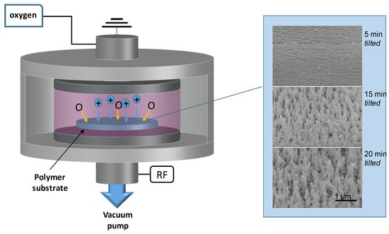
Figure 1.
A sketch illustrating a typical plasma nano-texturing process of a polymer. Scanning Electron Microscopy (SEM) tilted pictures of polycarbonate adapted with permission from [43]. Copyright 2011 John Wiley and Sons.
The strength of this process with respect to the others lies in the:
- Compatibility with the continuous roll to roll processing of polymer web;
- Speed; vacuum time could be an issue, but this is less relevant when a roll-to-roll process is optimized;
- No need for solvents; rather, it is a dry, eco-friendly method.
However, some issues of this approach, that can be overcome with suitable strategies, must be reported: (i) Being based on plasma etching, the process is highly dependent upon the substrate, hence it should be optimized for the specific polymer; e.g., silicone needs fluorocarbon (FC) gases, whereas for hydrocarbon polymers, oxygen plasma is best suited; (ii) The final nano-textured surface is contaminated by inorganic species; in fact, as mentioned before, and it will better described in Section 3, the key factor of this process is the controlled contamination of the surface; (iii) For a given polymer, the geometric dimensions of the engraved features are not independent: For example, each change in the experimental parameters leading to a taller structure will also lead to increasing the lateral dimension and spacing of the same. Solutions to the former two issues will be indicated in Section 3. However, for the latter, a trade-off should be found looking for the parameters (typically process time and power input) leading to the best nano-features aspect ratio for the specific surface property we want to address on the chosen polymer.
2. Plasma Nano-Texturing of Polymers: What?
Having detailed the reasons for the interest in plasma nano-texturing, we could discuss onto “what polymers could be treated and in which experimental conditions”. Plasma nano-texturing has been studied for a wide range of polymers, from hydrocarbons (polyethylene and polypropylene) to fluorocarbons (mostly polytetrafluoroethylene) and silicone ones. Table 2 summarizes some of the studies reported in literature, which are mostly grouped by polymer categories.
Table 2.
Examples of the plasma nano-texturing of different polymers, with indication of the gas feed and reactor configuration used. ICP stands for “inductive coupled plasma”.
One of the pioneer studies onto which the direct nano-texturing of polymers is concerned, was, in 1989, the oxygen plasma treatment of polytetrafluoroethylene (PTFE) to alter its wettability behavior [45]. Morra et al. observed that in a parallel plate, a capacitive coupled plasma (CCP) reactor, a rough surface appeared on PTFE which became more evident with increasing time. Much more, the introduction of a submicrometric scale texture made the polymer surface extremely hydrophobic with an advancing Water Contact Angle (WCA) close to 170° and a low hysteresis.
J.P. Youngblood et al. obtained a similar nano-texturing of a polymer, in this case Polypropylene (PP), using as source of etchant species a PTFE solid target, and feeding the plasma with a noble gas [46]. As a result of the ion sputtering of PTFE, the plasma resulted in becoming enriched in fluorine atoms that successfully etched PP, leading to the formation of nano-wrinkles for a process time higher than 30 min. In particular, they could get, in a one-step process, a water repellent surface with an advancing and receding WCA of 170° and 169°, respectively.
With a different approach, though in one step as well, Di Mundo et al. prepared super-hydrophobic nano-textured polystyrene (PS) pieces, optimizing the CF4/O2 gas flow rate ratio [47,48]. This gas mixture lead to the formation of submicrometric pillars (Figure 2) in a few minutes, but at a 17% content of oxygen in the feed, this allowed for the formation of a water repellent surface.
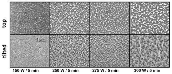
Figure 2.
SEM images of the polystyrene (PS) samples treated with a CF4/(17%)O2-fed discharge as a function of the power input. Adapted with permission from [47]. Copyright 2008 American Chemical Society.
These samples maintained their transparency to visible light, though longer treatment time lead to opaque surfaces because of the formation of larger micrometric features responsible for light scattering. In [48], they also proved the importance of coupling the right texturing size with a suitable chemical composition. Upon texturing, the surface chemistry was tuned in a wide range, depositing film by PECVD of an ethylene/c-C4F8 mixture with variable composition. Best performance in terms of a super-hydrophobic character was obtained with the most fluorinated coating, even if for texturing with taller nanofeatures, the chemical composition effect was less important.
Gogolides et al. deeply investigated the effect of the plasma nano-texturing of polymethyl-methacrylate (PMMA) [63,64,65,66,67]. The study was carried out with a radiofrequency-powered helicon reactor, with an auxiliary bias onto the sample holder. Depending on the final application, they kept the nano-textured surface uncoated, or they coated with an FC film (with a C4F8 PECVD). In this way, they could pass from super-hydrophilic surfaces, where proteins were effectively bonded for biosensing, to super-hydrophobic, textured surfaces, working as on-off valves when embedded in microfluidic devices, as illustrated in Figure 3. Since an issue for the microfluidic device, but also in other applications, can be the mechanical properties of the engraved nano-features, they also investigated the tribological properties of these surfaces [67]. Short plasma treatment time only slightly influenced mechanical and tribological properties of PMMA, whilst long process time had a detrimental effect. On the other hand, the deposition of the FC coating protected the nanopillars, reducing plastic deformation.
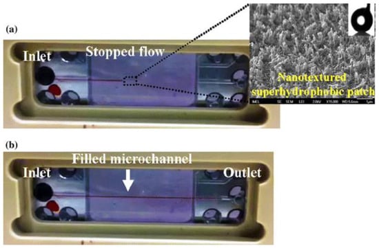
Figure 3.
Passive super-hydrophobic microvalve: The hydrophobic zone is placed in the middle of the microchannel (SEM image in the inset). (a) Stopped fluid flow (red dye) at the nano-textured hydrophobic zone, (b) filled microchannel upon valve opening. Reprinted with permission from [65]. Copyright 2014 Springer-Verlag Berlin Heidelberg.
Palumbo et al. optimized the plasma nano-texturing of polycarbonate (PC) [43,44]. As illustrated in Figure 1, as a consequence of O2 plasma, pillars are formed on the PC surface, with their height increasing with time and power input. Pillars had a lateral dimension in the range 20–80 nm, and a maximum height of about 1 μm. Soon after the treatment, the PC became very hydrophilic because of the introduction of new polar groups and the presence of nano-texturing. However, such behavior was not permanent; in 21 days the WCA of the modified polymer increased, losing the hydrophilic character for the typical hydrophobic recovery phenomenon. Notwithstanding this issue, the plasma deposition of a Teflon®-like or silicone-like coating contributed to produce water repellent surfaces. More interestingly, changing the chemistry of the organosilicon-based film deposited onto the nano-textured samples allowed for modulating the water condensation ability, and in particular, to obtain durable hydrophilic anti-fog surfaces as illustrated in Figure 4.
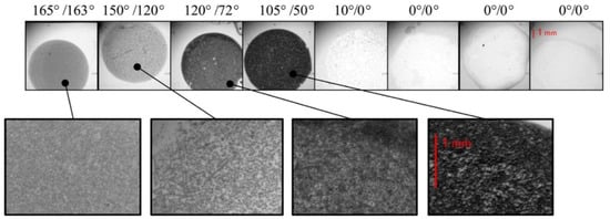
Figure 4.
Images of water condensed onto PC samples nano-textured with plasma etching and Plasma-Enhanced Chemical Vapor Deposition (PECVD), coated with different organosilicon-based films. Higher magnification images of the dropwise condensing (fogged) surfaces are shown below. Values of the advancing/receding Water Contact Angle (WCA) are reported at the top. Reproduced with permission from [44]. Copyright 2014 American Chemical Society.
Polydimetylsiloxane (PDMS) is an inexpensive elastomer often used for the production of protein microarrays in biosensing. Tserepi et al. modified PDMS-coated silicon and glass samples with a helicon plasma reactor under the application of a bias voltage onto the substrate [60,61,62]. Differently from the previous cases, being oxygen plasma inactive in ablating silicone-based polymers, the chosen feed was SF6. As shown in Figure 5, also in this, polymer pillars were engraved, with both height and lateral size linearly increasing with treatment time. The plasma nano-texturing largely affected the surface properties of PDMS with respect to protein immobilization. In particular, the protein microarrays produced onto these samples had a significantly higher spot signal intensity (3-fold) and intra-spot homogeneity (2-fold) with respect to commercially-available slides [62].
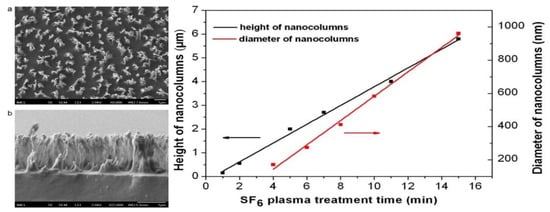
Figure 5.
SF6 plasma nano-textured PDMS. Left, (a) Top-down and (b) cross-section SEM images of a nano-textured polydimetylsiloxane (PDMS) surface obtained after a six min treatment under highly anisotropic conditions; Adapted with permission from [62]. Copyright 2010 Elsevier B.V. Right, evolution of the average height and diameter of nano-columns with process time; adapted with permission from [60]. Rights managed by AIP Publishing.
Plasma nano-texturing has been also optimized on less conventional polymers such as: Paper [54], dodecyl benzenesulfonate-doped polypyrrole (PPy(DBS)) [57], Polyethylenterephtalate (PET) fabric [58] and SU-8 photoresist [42].
Standard copy-grade paper and hand sheet control paper were both plasma etched in an oxygen plasma, and then coated with a 100 nm FC coating by PECVD [54]. As it can be observed in Figure 6I, such process can introduce nano-texturing in cellulose-based materials. Moreover, the paper wettability changed drastically: In particular, following this double step process, the paper resulted in being “roll-off” super-hydrophobic, while depositing the FC coating directly onto untreated cellulose, and due to the native micro-roughness of the material, the surface became “sticky” super-hydrophobic [79].
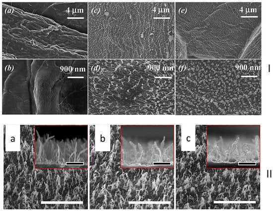
Figure 6.
(I) SEM images of (a,b) untreated, (c,d) oxygen-etched, and (e,f) oxygen-etched and FC-coated hand sheet fiber. Adapted with permission from [54]. Copyright 2008, American Chemical Society. (II) SEM images of oxygen plasma-etched dodecyl benzenesulfonate-doped polypyrrole (PPy(DBS)) surfaces without preheating (a), pre-heat treated at 100 °C (b) and pre-heat treated at 200 °C (c). The scale bars in the main images and the insets are 1 μm and 500 nm, respectively. Adapted with permission from [57]. Copyright 2017 American Chemical Society.
Jiang et al. studied the plasma nano-texturing of a polymer typically used in display, solar cells and similar optoelectronics application, PPy(DBS) [57]. They coated a silicon substrate with a Cr/Au layer, and then a PPy(DBS) layer, which was as thick as 4.7 μm, was electrodeposited on the top. Then the surface was nano-textured in an ICP reactor fed with oxygen. As it can be seen in Figure 6(II), the nano-texturing was successful with the formation of fibrils about 30 nm wide and with their length in the range 50 nm–1 μm (for a process time between 10 and 60 min). Furthermore, they evaluated the effect of heating the sample before the nano-texturing process, and no major changes were found onto the nanofibrils formation.
A super-hydrophobic PET fabric was modified by the addition of a nanotexture to the native micro-roughness of the fibers and combination with a low surface energy layer [58]. The deposition of a silicone-like coating on the innate micro-scale roughness of the woven fabric enhanced the hydrophobic character, but not enough: The maximum static WCA obtained was 144°, increasing with the density of filaments. Instead, a 1 min plasma nano-texturing was enough to form nanopillars on the fabric surface leading to water repellency once it had been coated with a silicone-like coating about 30 nm thick.
Stable super-hydrophobicity is better obtained forming hierarchical or dual scale (micro-/nano-) structures. Jose Marquez-Velasco et al. compared the wettability of flat and micro-patterned (by photolithography) SU-8 after plasma nano-texturing. The latter was achieved by O2 plasma in a helicon reactor and deposition of 15 nm FC coating [42]. They could produce nanopillars 2 μm high on patterned SU-8 in 5 min, as shown in Figure 7. They confirmed that the presence of both micro- and nano-features greatly enhanced the hydrophobic character.
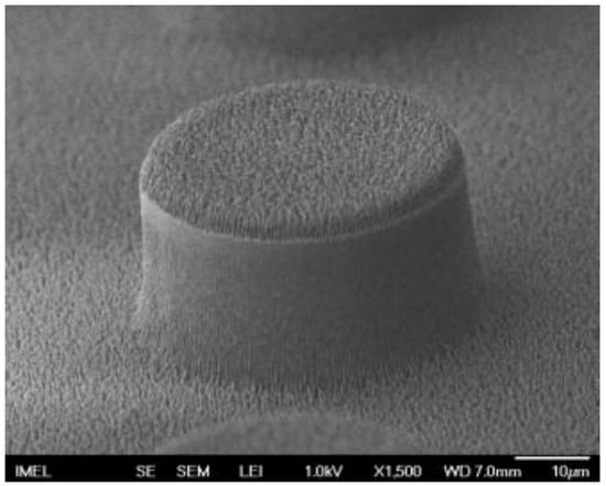
Figure 7.
Dual-scale topography of O2 plasma-treated micro-structured SU-8 surfaces (SEM image). Reproduced with permission from [42]. Copyright 2009 Elsevier B.V.
Many other examples of plasma nano-texturing can be found in Table 2, on other polymers like PEEK, Kapton and polyethylene, however here a last one should be mentioned. Di Mundo et al. extensively studied in the last years the oxygen plasma nano-texturing of PTFE [49,50,51,52]. The idea was to start from a bulky hydrophobic polymer to have a durable super-hydrophobic surface in a single plasma nano-texturing step. As illustrated in Figure 8, changing the RF power and the process time not only had an effect upon the size (as reported in the previously mentioned cases), but also on the shape of the submicrometric features. Namely, increasing time/power, the structures passed from a conic shape surmounted by hairy filaments (FS samples), to cones with spherical beads on the top (S-o-C samples). Here it is important to stress that such materials had a sharp super-hydrophobic behavior. Moreover, in water droplets bouncing experiments, authors showed that the contact time of the falling drop with the surface was very short for both the FS (200 W/10 min) and the S-o-C (300 W/15 min), being around 10.7 ms. However, increasing the impact speed, as expected, the contact time increased for the S-o-C, since the impact pressure increased, whereas for the FS samples it remained low. This was explained with the formation of stable air cavities underneath the filaments, as it has been reported for the Salvinia leaves [12], which are very similar in shape to the submicrometric features reported in this work (compare with the example reported in Table 1).
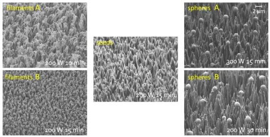
Figure 8.
SEM images of Teflon® surfaces treated by a self-masked, oxygen-fed plasma process. The effect of increasing the process time at constant power (200 W) is visible on the diagonal from the upper-left to the lower-right image. The effect of increasing the power at a constant process time (15 min) is shown on the diagonal from the lower-left to the upper-right image. Reproduced with permission from [50]. Copyright 2016 Elsevier.
3. Plasma Nano-Texturing Mechanism and Suggested Approach: How?
One main question remained open in this review: “how can plasma etching lead to the nano-texturing of polymers?”, or alternatively “what is the mechanism of plasma nano-texturing?”. If the mechanism is understood, likely it would be easier to optimize and control the plasma nano-texturing process on a specific polymer.
The first step to understand the main mechanism leading to direct plasma nano-texturing is the observation that, at the end of the process, the nano-textured polymer surface presented contamination of atoms different from the substrate and from the gas feed. Vourdas et al. found aluminum on nano-textured PMMA [63], while Palumbo et al. reported Cr and Fe contaminating PC upon plasma nano-texturing [43], and on PTFE just on the top of the nanostructures, in this case determined by means of energy-dispersive X-ray spectroscopy (EDX) map analysis, as reported in Figure 9 [52]. A similar metal contamination was identified by Ko et al. onto nano-textured PMMA, PET, Carbon fiber and diamond [69].
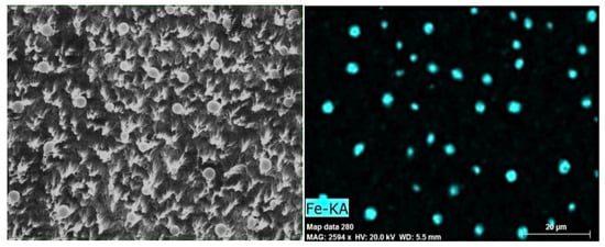
Figure 9.
SEM image (left) and corresponding Scanning Electron Microscopy-Energy-dispersive X-ray spectroscopy (SEM-EDX) map of iron (right) of a polytetrafluoroethylene (PTFE) sample treated by plasma at 300 W for 15 min. Adapted with permission from [52]. Copyright 2019 Elsevier B.V.
In the case of [63], the ICP chamber had an alumina dome, while in the other examples, it was a capacitive coupled reactor in a stainless steel chamber and electrodes, in both cases materials compatible with the found contaminations. Ko et al. in another paper showed that if the electrode sample holder was covered by a PS plate, no pillars could be found using the same experimental conditions, usually leading to the nano-texturing of PET [68]. In an analogous experiment, but on the ICP plasma reactor, by covering the alumina dome with a thick carbon-containing polymer coating, plasma nano-texturing was greatly reduced. These outcomes support the idea that the metal-containing species which sputtered from the electrodes and reactor walls contaminates the sample with unvolatile nanoclusters. On the other hand, when the emitting parts are covered with C-containing polymers, the species contaminating the sample are carbonaceous, hence they can be easily removed from the surface by the same running plasma etching process.
Keeping in mind this observation we can describe the mechanism according to the scheme reported in Figure 10 [63,68,69,74,77]. When a plasma is ignited in presence of a polymer and of a gas feed, producing a suitable etchant species for that sample, conventional plasma etching starts by the formation of volatile species, and the polymer surface is eroded. At the same time, ions from the plasma are accelerated onto the electrodes and walls causing the sputtering of inorganic/metal species that deposit onto the sample surface (a). Such species cannot be ablated and consumed in the experimental conditions used (gas feed being typically oxygen, CF4 and SF6), and they assemble a sort of nano-mask with respect to the arriving etchant species (b). Hence, the etching process of the polymer, assisted by the impinging ions, can proceed only through the apertures between the inorganic clusters (c).
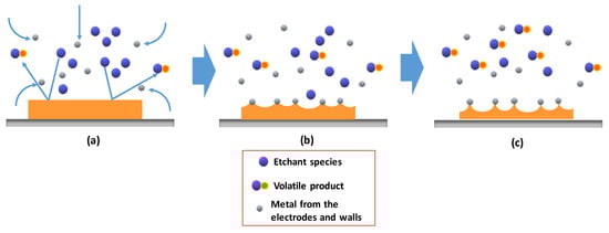
Figure 10.
Schematized mechanism of the plasma nano-texturing of polymers. (a) plasma ignition, etchant species producing volatile species; (b) during plasma etching metal clusters stick on the sample, masking the surface; (c) Etching proceed though the nanomask.
Even if the process leads to high aspect ratio pillar/filaments, the etching process has an important isotropic contribution, as it can be observed from the roundish shape in the inter-feature regions, see Figure 2, Figure 3 and Figure 5. This is also confirmed by the increasing distance between the pillars when the etching time is prolonged (Figure 1). The observation that the nano-features’ height increases with process time and input power is obviously due to the longer exposure to and higher content of etchant species.
A confirmation of the explained mechanism comes from the analogies indicated in the formation of “Black Silicon” during processes of Deep Reactive-ion Etching (RIE) [80]. SF6 gas is used as the main etchant of silicon, and the addition of O2 leads to the production of non-volatile silicon-oxy-halogens (SiOxFy), where such species randomly settle on the silicon sample and only the unmasked areas on the silicon can be etched. The RIE process typically involves alternating “etching” and “deposition” of the silicon substrate. In this specific process a sidewall passivation of the structures develops, leading to high aspect ratio of the nanofeatures, see Figure 11.
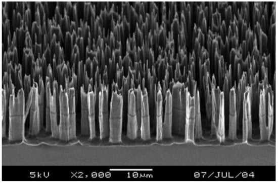
Figure 11.
“Black silicon” formed during a reactive-ion Etching (RIE) process of silicon. Adapted with permission from [80]. Copyright 2009 IOP publishing.
Another point can be considered in the mechanism. If a fluorine-containing gas is used for the plasma nano-texturing of an organic polymer, the engraving process is accompanied by the grafting of F atoms, often leading to a substantial decrease in the water wettability. This has been observed in the nano-texturing of polystyrene by plasma fed with an O2/CF4 gas mixture, [47] or in the case of SU-8 etching in perfluoromethane plasma [59].
The role of the metal sputtering deserves a further comment. Being the sputtering of electrodes and the wall reactor, a crucial step in plasma nano-texturing, the resulting treated surface is contaminated, and this could be an undesired effect for some specific applications. Consider that the main application is often the production of water-repellent surfaces: In this case, as deeply described in Section 2, a hydrophobic coating is commonly added, with the additional effect of covering the contaminating material. In fact, it is quite easy to deposit Teflon®-like coatings by low pressure plasma fed with fluorocarbon, also in the same reactor [48,65] or, as an alternative, silicone-like films from organosilicon-fed plasma, just to keep an all dry process. Less straightforward, instead, is to use texturing to get a stable super-hydrophilic surface. In fact, once a polymer surface is transformed into hydrophilic in a matter of days it recovers the original wettability, or most of that. Such phenomenon is known as hydrophobic recovery, and it is based mostly upon the natural mobility of the polymer chains, whose displacement attempts to reduce energy by burying the polar groups [81,82]. In this case a possible approach is to deposit an inorganic coating, as described in the previous section for [43,44]. On the other hand, it has been proven that long treatment time in O2 plasma, 20 min or higher, leads to stable (20 days or more) super-hydrophilic surfaces, as demonstrated for PMMA and PEEK. This can be due to more extensive grafting of functional groups, and higher amount of hydrophilic contaminating clusters. Furthermore, it should be considered that aging is partly hidden by the nano-texturing, leading always to a lowering of the WCA of hydrophilic surfaces.
In other examples some approaches have being investigated for “controlling” the contamination. This was the case reported by Schulz et al., that turned the direct process in a double step one [83]: The first step consisted in the very short evaporation of the silicon or titanium dioxide non-continuous layer. The role of this step was to deposit a specific random nano-mask, through which the following O2 plasma etching (in electrodes/wall sputtering-free conditions) could engrave the nanopillars. The authors succeeded with this approach to nanotexture PMMA, thus increasing its optical transmittance.
In another elegant work it has been shown that PET can be plasma nano-textured using a specific metal contamination, notwithstanding the nature of reactor electrodes and walls [68]. The reactor was a capacitively coupled one, so the authors completely covered the bottom electrode holder with a well-defined metal (Ag, Cu, Pt and Si). In this way, in one single process, they could obtain nano-textured PET with specific metal nanoparticles on top of the structures, with potential photonic applications.
4. Conclusions
The aim of this review was to illustrate the versatility of plasma nano-texturing. Nano-features with high aspect ratio can be engraved in polymers of different nature, hydrocarbon, fluorocarbon or silicone-based, with a mask-less, one-step process.
To summarize:
- Most of the common hydrocarbon or acrylate/ester polymers (PMMA, PET) and alike, can be efficiently nano-textured in O2 plasma in CCP or ICP reactors.
- Also F-containing feed, such as CF4 or SF6, can be used with such polymers; in this case, since scarcely polarizable C–F bonds are formed, the WCA can increase, and in some cases the surface becomes super-hydrophobic.
- Silicone-based polymers, having an O–Si–O backbone, can be plasma nano-textured only in fluorinated feed (chlorine-based could likely work as well, but it has not been proposed for the disadvantages of handling such a process).
- Plasma nano-texturing brings the advantages of high throughput processing with low environmental impact.
- It is compatible with following procedures to add additional properties to the surface: For example, plasma deposition of low surface energy coatings for a water repellent surface, or stable hydrophilic film, or functionalized for biosensing and alike.
- The mechanism has been illustrated; the process, though very reproducible, depends on the contamination of the polymer surface during the plasma etching. This could be a drawback, if for the intended application, the inorganic contamination represents a problem, but several solutions have been indicated to overcome this issue.
Funding
This research received no external funding
Acknowledgments
Rosa Di Mundo is grateful acknowledged for the fruitful discussion on this subject. Valeria Veronico and Mariagrazia Troia are acknowledged for to their support.
Conflicts of Interest
The authors declare no conflict of interest.
References
- Bhushan, B. Biomimetics: Lessons from Nature—An overview. Philos Trans. R Soc. A Math. Phys. Eng. Sci. 2009, 367, 1445–1486. [Google Scholar] [CrossRef]
- Mukherjee, A. Biomimetics Learning from Nature; IntechOpen: London, UK, 2010. [Google Scholar]
- Huang, J.; Wang, X.; Wang, Z.L. Controlled replication of butterfly wings for achieving tunable photonic properties. Nano Lett. 2006, 6, 2325–2331. [Google Scholar] [CrossRef]
- Baryshnikova, K.V.; Kadochkin, A.S.; Shalin, A.S. Nanostructural antireflecting coatings: Classification analysis (A review). Opt. Spectrosc. 2015, 119, 343–355. [Google Scholar] [CrossRef]
- Chen, H.; Zhang, X.; Ma, L.; Che, D.; Zhang, D.; Sudarshan, T.S. Investigation on large-area fabrication of vivid shark skin with superior surface functions. Appl. Surf. Sci. 2014, 316, 124–131. [Google Scholar] [CrossRef]
- Yamamoto, M.; Nishikawa, N.; Mayama, H.; Nonomura, Y.; Yokojima, S.; Nakamura, S.; Uchida, K. Theoretical Explanation of the Lotus Effect: Superhydrophobic Property Changes by Removal of Nanostructures from the Surface of a Lotus Leaf. Langmuir 2015, 31, 7355–7363. [Google Scholar] [CrossRef]
- Bixler, G.D.; Bhushan, B. Bioinspired rice leaf and butterfly wing surface structures combining shark skin and lotus effects. Soft Matter 2012, 8, 11271–11284. [Google Scholar] [CrossRef]
- Guadarrama-Cetina, J.; Mongruel, A.; Medici, M.G.; Baquero, E.; Parker, A.R.; Milimouk-Melnytchuk, I.; González-Viñas, W.; Beysens, D. Dew condensation on desert beetle skin. Eur. Phys. J. E 2014, 37, 109. [Google Scholar] [CrossRef]
- Feng, L.; Zhang, Y.; Xi, J.; Zhu, Y.; Wang, N.; Xia, F.; Jiang, L. Petal effect: A superhydrophobic state with high adhesive force. Langmuir 2008, 24, 4114–4119. [Google Scholar] [CrossRef]
- Gao, H.; Wang, X.; Yao, H.; Gorb, S.; Arzt, E. Mechanics of hierarchical adhesion structures of geckos. Mech. Mater. 2005, 37, 275–285. [Google Scholar] [CrossRef]
- Jiang, L.; Gao, X. Water-repellent legs of water striders. Nature 2004, 432, 36. [Google Scholar] [CrossRef]
- Barthlott, W.; Schimmel, T.; Wiersch, S.; Koch, K.; Brede, M.; Barczewski, M.; Walheim, S.; Weis, A.; Kaltenmaier, A.; Leder, A.; et al. The salvinia paradox: Superhydrophobic surfaces with hydrophilic pins for air retention under water. Adv. Mater. 2010, 22, 2325–2328. [Google Scholar] [CrossRef] [PubMed]
- Gao, L.; McCarthy, T.J. How Wenzel and Cassie were wrong. Langmuir 2007, 23, 3762–3765. [Google Scholar] [CrossRef] [PubMed]
- Gao, L.; Mccarthy, T.J. Versus Tensile Hydrophobicity and Wettability Characterization. Langmuir 2008, 24, 546–550. [Google Scholar] [CrossRef]
- Marmur, A.; Bittoun, E. When wenzel and cassie are right: Reconciling local and global considerations. Langmuir 2009, 25, 1277–1281. [Google Scholar] [CrossRef]
- Yildirim Erbil, H.; Elif Cansoy, C. Range of applicability of the wenzel and cassie-baxter equations for superhydrophobic surfaces. Langmuir 2009, 25, 14135–14145. [Google Scholar] [CrossRef]
- Quéré, D. Rough ideas on wetting. Phys. Stat. Mech. Appl. 2002, 313, 32–46. [Google Scholar] [CrossRef]
- Wen, L.; Weaver, J.C.; Thornycroft, P.J.M.; Lauder, G.V. Hydrodynamic function of biomimetic shark skin: Effect of denticle pattern and spacing. Bioinspiration Biomim. 2015, 10, 066010. [Google Scholar] [CrossRef]
- Biswas, A.; Bayer, I.S.; Biris, A.S.; Wang, T.; Dervishi, E.; Faupel, F. Advances in top-down and bottom-up surface nanofabrication: Techniques, applications & future prospects. Adv. Colloid. Interface Sci. 2012, 170, 2–27. [Google Scholar] [CrossRef]
- Liddle, J.A.; Gallatin, G.M. Nanomanufacturing: A Perspective. ACS Nano 2016, 10, 2995–3014. [Google Scholar] [CrossRef]
- Persano, L.; Camposeo, A.; Pisignano, D. Active polymer nanofibers for photonics, electronics, energy generation and micromechanics. Prog. Polym. Sci. 2015, 43, 48–95. [Google Scholar] [CrossRef]
- DiBenedetto, S.A.; Facchetti, A.; Ratner, M.A.; Marks, T.J. Molecular self-assembled monolayers and multilayers for organic and unconventional inorganic thin-film transistor applications. Adv. Mater. 2009, 21, 1407–1433. [Google Scholar] [CrossRef]
- King, D.M.; Johnson, S.I.; Li, J.; Du, X.; Liang, X.; Weimer, A.W. Atomic layer deposition of quantum-confined ZnO nanostructures. Nanotechnology 2009, 20, 195401. [Google Scholar] [CrossRef] [PubMed]
- Weatherspoon, M.R.; Cai, Y.; Crne, M.; Srinivasarao, M.; Sandhage, K.H. 3D rutile titania-based structures with Morpho butterfly wing scale morphologies. Angew. Chem. Int. Ed. 2008, 47, 7921–7923. [Google Scholar] [CrossRef] [PubMed]
- Choi, S.W.; Park, J.Y.; Kim, S.S. Synthesis of SnO2-ZnO core-shell nanofibers via a novel two-step process and their gas sensing properties. Nanotechnology 2009, 20, 465603. [Google Scholar] [CrossRef] [PubMed]
- Kuzuya, A.; Komiyama, M. DNA origami: Fold, stick, and beyond. Nanoscale 2010, 2, 310–322. [Google Scholar] [CrossRef] [PubMed]
- Clough, R.L. High-energy radiation and polymers: A review of commercial processes and emerging applications. Nucl. Instrum. Methods Phys. Res. Sect. B Beam. Interact. Mater. Atoms. 2001, 185, 8–33. [Google Scholar] [CrossRef]
- Whitesides, G.M.; Stroock, A.D. Flexible methods for microfluidics. Phys. Today 2001, 54, 42. [Google Scholar] [CrossRef]
- Chou, S.Y.; Krauss, P.R.; Zhang, W.; Guo, L.; Zhuang, L. Imprint Lithography with 25-Nanometer Resolution. J. Vac. Sci. Technol. B. 1997, 15, 2897–2904. [Google Scholar] [CrossRef]
- Park, S.; Lee, D.H.; Xu, J.; Kim, B.; Hong, S.W.; Jeong, U.; Xu, T.; Russell, T.P. Macroscopic 10 Terabit/in2 Arrays from Block Copolymers with Lateral Order. Science 2009, 323, 1030. [Google Scholar] [CrossRef]
- Yıldırım Erbil, H.; Levent Demirel, A.; Yonca Avciı, O.M. Transformation of a Simple Plastic into a Superhydrophobic Surface. Science 2003, 299, 1377–1380. [Google Scholar] [CrossRef]
- Chapman, B. Glow Discharge Processes Sputtering and Plasma Etching; John Wiley & Sons: New York, NY, USA, 1980. [Google Scholar]
- D’agostino, R. (Ed.) Plasma Deposition, Treatment and Etching of Polymers; Academic Press: San Diego, CA, USA, 1990; Available online: http://www.sciencedirect.com/science/article/pii/B9780122004308500130 (accessed on 30 September 2019).
- Balazs, D.J.; Hollenstein, C.; Mathieu, H.J. Fluoropolymer coating of medical grade poly(vinyl chloride) by plasma-enhanced chemical vapor deposition techniques. Plasma Process Polym. 2005, 2, 104–111. [Google Scholar] [CrossRef]
- Coclite, A.M.; Milella, A.; d’Agostino, R.; Palumbo, F. On the relationship between the structure and the barrier performance of plasma deposited silicon dioxide-like films. Surf. Coat. Technol. 2010, 204, 4012–4017. [Google Scholar] [CrossRef]
- Achard, J.; Tallaire, A.; Sussmann, R.; Silva, F.; Gicquel, A. The control of growth parameters in the synthesis of high-quality single crystalline diamond by CVD. J. Cryst. Growth. 2005, 284, 396–405. [Google Scholar] [CrossRef]
- Trizio, I.; Garzia Trulli, M.; Lo Porto, C.; Pignatelli, D.; Camporeale, G.; Palumbo, F.; Sardella, E.; Gristina, R.; Favia, P. Plasma Processes for Life Sciences. In Reference Module in Chemistry, Molecular Sciences and Chemical Engineering; Reedijk, J., Ed.; Elsevier Inc.: Amsterdam, The Netherlands, 2018; pp. 1–24. [Google Scholar] [CrossRef]
- Fracassi, F.; D’Agostino, R.; Palumbo, F.; Bellucci, F.; Monetta, T. Deposition of gold-containing siloxane thin films. Thin Solid Films 1996, 272, 61–63. [Google Scholar] [CrossRef]
- Kurdi, J.; Ardelean, H.; Marcus, P.; Jonnard, P.; Arefi-Khonsari, F. Adhesion properties of aluminium-metallized/ammonia plasma-treated polypropylene—Spectroscopic analysis (XPS, EXES) of the aluminium/polypropylene interface. Appl. Surf. Sci. 2002, 189, 119–128. [Google Scholar] [CrossRef]
- Cicala, G.; Creatore, M.; Favia, P.; Lamendola, R.; D’Agostino, R. Modulated rf discharges as an effective tool for selecting excited species. Appl. Phys. Lett. 1999, 75, 37–39. [Google Scholar] [CrossRef]
- Phan, L.T.; Yoon, S.M.; Moon, M.W. Plasma-based nanostructuring of polymers: A review. Polymers 2017, 9, 417. [Google Scholar] [CrossRef]
- Marquez-Velasco, J.; Vlachopoulou, M.E.; Tserepi, A.; Gogolides, E. Stable superhydrophobic surfaces induced by dual-scale topography on SU-8. Microelectron. Eng. 2010, 87, 782–785. [Google Scholar] [CrossRef]
- Palumbo, F.; Di Mundo, R.; Cappelluti, D.; d’Agostino, R. SuperHydrophobic and SuperHydrophilic polycarbonate by tailoring chemistry and nano-texture with plasma processing. Plasma Process Polym. 2011, 8, 118–126. [Google Scholar] [CrossRef]
- Di Mundo, R.; d’Agostino, R.; Palumbo, F. Long-lasting antifog plasma modification of transparent plastics. ACS Appl. Mater. Interfaces 2014, 6, 17059–17066. [Google Scholar] [CrossRef]
- Morra, M.; Occhiello, E.; Garbassi, F. Contact angle hysteresis in oxygen plasma treated poly(tetrafluoroethylene). Langmuir 1989, 5, 872–876. [Google Scholar] [CrossRef]
- Youngblood, J.P.; McCarthy, T.J. Ultrahydrophobic polymer surfaces prepared by simultaneous ablation of polypropylene and sputtering of poly(tetrafluoroethylene) using radio frequency plasma. Am. Chem. Soc. Polym. Prepr. Div. Polym. Chem. 1999, 40, 563–564. [Google Scholar] [CrossRef]
- Di Mundo, R.; Palumbo, F.; D’Agostino, R. Nanotexturing of polystyrene surface in fluorocarbon plasmas: From sticky to slippery superhydrophobicity. Langmuir 2008, 24, 5044–5051. [Google Scholar] [CrossRef]
- Di Mundo, R.; Palumbo, F.; D’Agostino, R. Influence of chemistry on wetting dynamics of nanotextured hydrophobic surfaces. Langmuir 2010, 26, 5196–5201. [Google Scholar] [CrossRef]
- Di Mundo, R.; Bottiglione, F.; Palumbo, F.; Favia, P.; Carbone, G. Sphere-on-cone microstructures on Teflon surface: Repulsive behavior against impacting water droplets. Mater. Des. 2016, 92, 1052–1061. [Google Scholar] [CrossRef]
- Di Mundo, R.; Bottiglione, F.; Palumbo, F.; Notarnicola, M.; Carbone, G. Filamentary superhydrophobic Teflon surfaces: Moderate apparent contact angle but superior air-retaining properties. J. Colloid Interface Sci. 2016, 482, 175–182. [Google Scholar] [CrossRef]
- Di Mundo, R.; Bottiglione, F.; Notarnicola, M.; Palumbo, F.; Pascazio, G. Plasma-textured teflon: Repulsion in air of water droplets and drag reduction underwater. Biomimetics 2017, 2, 1. [Google Scholar] [CrossRef]
- Lo Porto, C.; Di Mundo, R.; Veronico, V.; Trizio, I.; Barucca, G.; Palumbo, F. Easy plasma nano-texturing of PTFE surface: From pyramid to unusual spherules-on-pyramid features. Appl. Surf. Sci. 2019, 483, 60–68. [Google Scholar] [CrossRef]
- Byun, D.; Lee, Y.; Tran, S.B.Q.; Nugyen, V.D.; Kim, S.; Park, B.; Lee, S.; Inamdar, N.; Bau, H.H. Electrospray on superhydrophobic nozzles treated with argon and oxygen plasma. Appl. Phys. Lett. 2008, 92, 1–4. [Google Scholar] [CrossRef]
- Balu, B.; Breedveld, V.; Hess, D.W. Fabrication of “roll-off” and “sticky” superhydrophobic cellulose surfaces-via plasma processing. Langmuir 2008, 24, 4785–4790. [Google Scholar] [CrossRef]
- Woodward, I.; Schofield, W.C.E.; Roucoules, V.; Badyal, J.P.S. Super-hydrophobic surfaces produced by plasma fluorination of polybutadiene films. Langmuir 2003, 19, 3432–3438. [Google Scholar] [CrossRef]
- Li, Y.P.; Lei, M.K. Nanotexturing and wettability ageing of polypropylene surfaces modified by oxygen capacitively coupled radio frequency plasma. J. Mater. Sci. Technol. 2014, 30, 965–972. [Google Scholar] [CrossRef]
- Jiang, Y.; Xu, J.; Lee, J.; Du, K.; Yang, E.H.; Moon, M.W.; Choi, C.H. Nanotexturing of Conjugated Polymers via One-Step Maskless Oxygen Plasma Etching for Enhanced Tunable Wettability. Langmuir 2017, 33, 6885–6894. [Google Scholar] [CrossRef]
- Park, S.; Kim, J.; Park, C.H. Influence of micro and nano-scale roughness on hydrophobicity of a plasma-treated woven fabric. Text Res. J. 2017, 87, 193–207. [Google Scholar] [CrossRef]
- Park, S.G.; Moon, J.H.; Lee, S.K.; Shim, J.; Yang, S.M. Bioinspired holographically featured superhydrophobic and supersticky nanostructured materials. Langmuir 2010, 26, 1468–1472. [Google Scholar] [CrossRef]
- Vlachopoulou, M.E.; Petrou, P.S.; Kakabakos, S.E.; Tserepi, A.; Gogolides, E. High-aspect-ratio plasma-induced nanotextured poly(dimethylsiloxane) surfaces with enhanced protein adsorption capacity. J. Vac. Sci. Technol. B Microelectron. Nanom. Struct. 2008, 26, 2543–2548. [Google Scholar] [CrossRef]
- Tserepi, A.D.; Vlachopoulou, M.E.; Gogolides, E. Nanotexturing of poly(dimethylsiloxane) in plasmas for creating robust super-hydrophobic surfaces. Nanotechnology 2006, 17, 3977–3983. [Google Scholar] [CrossRef]
- Vlachopoulou, M.E.; Tserepi, A.; Petrou, P.S.; Gogolides, E.; Kakabakos, S.E. Protein arrays on high-surface-area plasma-nanotextured poly(dimethylsiloxane)-coated glass slides. Colloids Surf. B Biointerfaces 2011, 83, 270–276. [Google Scholar] [CrossRef]
- Vourdas, N.; Tserepi, A.; Gogolides, E. Nanotextured super-hydrophobic transparent poly(methyl methacrylate) surfaces using high-density plasma processing. Nanotechnology 2007, 18, 125304–125311. [Google Scholar] [CrossRef]
- Tsougeni, K.; Tserepi, A.; Constantoudis, V.; Gogolides, E.; Petrou, P.S.; Kakabakos, S.E. Plasma nanotextured PMMA surfaces for protein arrays: Increased protein binding and enhanced detection sensitivity. Langmuir 2010, 26, 13883–13891. [Google Scholar] [CrossRef]
- Ellinas, K.; Tserepi, A.; Gogolides, E. Superhydrophobic, passive microvalves with controllable opening threshold: Exploiting plasma nanotextured microfluidics for a programmable flow switchboard. Microfluid. Nanofluidics 2014, 17, 489–498. [Google Scholar] [CrossRef]
- Gnanappa, A.K.; Papageorgiou, D.P.; Gogolides, E.; Tserepi, A.; Papathanasiou, A.G.; Boudouvis, A.G. Hierarchical, plasma nanotextured, robust superamphiphobic polymeric surfaces structurally stabilized through a wetting-drying cycle. Plasma Process Polym. 2012, 9, 304–315. [Google Scholar] [CrossRef]
- Skarmoutsou, A.; Charitidis, C.A.; Gnanappa, A.K.; Tserepi, A.; Gogolides, E. Nanomechanical and nanotribological properties of plasma nanotextured superhydrophilic and superhydrophobic polymeric surfaces. Nanotechnology 2012, 23, 505711–505722. [Google Scholar] [CrossRef] [PubMed]
- Ko, T.J.; Oh, K.H.; Moon, M.W. Plasma-Induced Hetero-Nanostructures on a Polymer with Selective Metal Co-Deposition. Adv. Mater. Interfaces 2015, 2, 1–8. [Google Scholar] [CrossRef]
- Ko, T.J.; Jo, W.; Lee, H.J.; Oh, K.H.; Moon, M.W. Nanostructures formed on carbon-based materials with different levels of crystallinity using oxygen plasma treatment. Thin Solid Films 2015, 590, 324–329. [Google Scholar] [CrossRef]
- Teshima, K.; Sugimura, H.; Inoue, Y.; Takai, O.; Takano, A. Transparent ultra water-repellent poly(ethylene terephthalate) substrates fabricated by oxygen plasma treatment and subsequent hydrophobic coating. Appl. Surf. Sci. 2005, 244, 619–622. [Google Scholar] [CrossRef]
- Fresnais, J.; Chapel, J.P.; Poncin-Epaillard, F. Synthesis of transparent superhydrophobic polyethylene surfaces. Surf. Coat. Technol. 2006, 200, 5296–5305. [Google Scholar] [CrossRef]
- Li, Y.P.; Li, S.Y.; Shi, W.; Lei, M.K. Hydrophobic over-recovery during aging of polyethylene modified by oxygen capacitively coupled radio frequency plasma: A new approach for stable superhydrophobic surface with high water adhesion. Surf. Coat. Technol. 2012, 206, 4952–4958. [Google Scholar] [CrossRef]
- Tsougeni, K.; Papageorgiou, D.; Tserepi, A.; Gogolides, E. “Smart” polymeric microfluidics fabricated by plasma processing: Controlled wetting, capillary filling and hydrophobic valving. Lab Chip 2010, 10, 462–469. [Google Scholar] [CrossRef]
- Tsougeni, K.; Vourdas, N.; Tserepi, A.; Gogolides, E.; Cardinaud, C. Mechanisms of oxygen plasma nanotexturing of organic polymer surfaces: From stable super hydrophilic to super hydrophobic surfaces. Langmuir 2009, 25, 11748–11759. [Google Scholar] [CrossRef]
- Morber, J.R.; Wang, X.; Liu, J.; Snyder, R.L.; Wang, Z.L. Wafer-level patterned and aligned polymer nanowire/micro- and nanotube arrays on any substrate. Adv. Mater. 2009, 21, 2072–2076. [Google Scholar] [CrossRef]
- Du, K.; Wathuthanthri, I.; Liu, Y.; Kang, Y.T.; Choi, C.H. Fabrication of polymer nanowires via maskless O2 plasma etching. Nanotechnology 2014, 25, 165301–165311. [Google Scholar] [CrossRef] [PubMed]
- Chen, M.H.; Chuang, Y.J.; Tseng, F.G. Self-masked high-aspect-ratio polymer nanopillars. Nanotechnology 2008, 19, 505301–505308. [Google Scholar] [CrossRef] [PubMed]
- Gogolides, E.; Constantoudis, V.; Kokkoris, G.; Kontziampasis, D.; Tsougeni, K.; Boulousis, G.; Vlachopoulou, M.; Tserepi, A. Controlling roughness: From etching to nanotexturing and plasma-directed organization on organic and inorganic materials. J. Phys. D Appl. Phys. 2011, 44, 174021–174034. [Google Scholar] [CrossRef]
- Palumbo, F.; Di Mundo, R. Wettability: Significance and measurement. In Polymer Surface Characterization; Sabbatini, L., Ed.; Walter de Gruyter Gmbh: Berlin, Germany; Boston, MA, USA, 2014; pp. 207–245. [Google Scholar]
- Jansen, H.V.; De Boer, M.J.; Unnikrishnan, S.; Louwerse, M.C.; Elwenspoek, M.C. Black silicon method X: A review on high speed and selective plasma etching of silicon with profile control: An in-depth comparison between Bosch and cryostat DRIE processes as a roadmap to next generation equipment. J. Micromech. Microeng. 2009, 19, 033001–033042. [Google Scholar] [CrossRef]
- Occhiello, E.; Morra, M.; Cinquina, P.; Garbassi, F. Hydrophobic recovery of oxygen-plasma-treated polystyrene. Polymer (Guildf) 1992, 33, 3007–3015. [Google Scholar] [CrossRef]
- Fritz, J.L.; Owen, M.J. Hydrophobic recovery of plasma-treated polydimethylsiloxane. J. Adhes. 1995, 54, 33–45. [Google Scholar] [CrossRef]
- Schulz, U.; Munzert, P.; Leitel, R.; Wendling, I.; Kaiser, N.; Tünnermann, A. Antireflection of transparent polymers by advanced plasma etching procedures. Opt. Express 2007, 15, 13108–13113. [Google Scholar] [CrossRef]


© 2019 by the authors. Licensee MDPI, Basel, Switzerland. This article is an open access article distributed under the terms and conditions of the Creative Commons Attribution (CC BY) license (http://creativecommons.org/licenses/by/4.0/).