Article

Comparison of the Optical and Electrical Properties of Al-Doped ZnO Films Using a Lorentz Model

1
Department of Physics, Fu Jen Catholic University, No.510 Zhongzheng Rd., Xinzhuang Dist., New Taipei City 24205, Taiwan
2
Graduate Institute of Applied Science and Engineering, Fu Jen Catholic University, No. 510 Zhongzheng Rd., Xinzhuang Dist., New Taipei City 24205, Taiwan
*
Author to whom correspondence should be addressed.
Coatings 2019, 9(1), 4; https://doi.org/10.3390/coatings9010004
Submission received: 29 October 2018 / Revised: 9 December 2018 / Accepted: 17 December 2018 / Published: 21 December 2018
(This article belongs to the Special Issue Design, Manufacturing and Measurement of Optical Film Coatings)

Abstract

:
In this research, zinc oxide (ZnO) films are doped with various amounts of Al dopants, from 0 to 13 at.%, using ion-beam co-sputtering for Zn and Al metallic targets at room temperature. The Al-doped ZnO (AZO) films appear to have lower transmittances in the UV and near-IR ranges. The electrical and optical properties of each film are successfully analyzed by using the spectroscopic ellipsometry of two Lorentz oscillators for the two lower transmittances. The optimal AZO film is deposited with an Al-dopant of 1.5 at.% at an oxygen partial pressure of 0.12 mTorr; it has the smallest resistivity of 7.8 × 10⁻⁴ Ω cm and high transmittance of > 80% in the visible regions. The free carrier concentration and mobility evaluated using ellipsometry are different from those measured using the Hall effect. This phenomenon was the result of the grain boundary scattering due to the small ~20-nm grain size of the AZO film used in this study.

1. Introduction

Conductive transparent oxide (CTO) films have high transmittance in the visible light region and high reflectance in the IR region in combination with a high conductivity; therefore, they are widely used in electronic and optical devices. Zinc oxide (ZnO) film, a CTO film, has a hexagonal wurtzite structure [1]. It is an n-type semiconductor and has a direct wide bandgap of approximately 3.4 eV. The existence of electron carriers is due to oxygen vacancies and intrinsic defects [2,3]. ZnO films exhibit high visible transparency and low resistivity, which, however, is still greater than that of indium tin oxide (ITO). The Al dopant, a group-III element, has become the most promising n-type semiconductor candidate because of its high thermal stability [4,5,6,7]. Al-doped ZnO (AZO) film has played a significant role in the development of optoelectronic devices [8,9,10,11]. It is not only highly visible transparent but also has metal-like electrical conductivity [1]. Many researchers have evaluated its optical and electrical properties. Spectroscopic ellipsometry is one of the methods used to determine the thickness, surface roughness, and optical constants using various dispersion models [12,13,14].
This study includes reviewed data from our previous studies [15,16,17,18,19], wherein AZO films were investigated using spectroscopic ellipsometry with a parametric model containing two Lorentz oscillators. The model assumes that the response of the electron carrier driven by the electric field in the film is similar to that of a mass harmonically driven by a spring combined with a dissipative force. In this comparison, the spring represents the electrostatic force on the electron caused by all the other electrons and nuclei in the solid, and the dissipative force represents the energy loss due to the emission of a photon. This model treats the electron as a particle that has mass orbits with a given trajectory and a certain amount of kinetic energy. Although this model violates the allowed quantum energy level, the Lorentz model still accurately depicts the optical constants of many optical materials and resonant absorptive processes.
The optical spectrum exhibits two lower transmittances in the near-IR range due to the conductive property of the electron carriers in the AZO film, and in the UV range due to the dielectric property of the optical absorption. The Lorentz oscillator for the zero-energy-centered free electron absorption in the near-IR range is usually reduced to the Drude model, which is very useful for transparent conductive oxides [20]. Thus, in this study, we used a parametric model with two Lorentz oscillators for the optical dispersion, instead of using Cauchy and Drude models [12], to methodically investigate AZO films doped with various amounts of Al. A comparison of the conductive properties, obtained from Hall effect measurements and from spectroscopic ellipsometry measurements in the near-IR range, reveals that the motions of the free carriers driven by the constant electric Lorentz force and by the alternate electromagnetic wave scatters differently on the AZO film [21,22].

2. Materials and Methods

2.1. Sample Preparation

In our previously published articles, the apparatus for the ion-beam sputtering system included an ion source, as shown in Figure 1. Both high-purity zinc and aluminum metal targets were mounted side by side on a water-cooled copper block. By adjusting the distance H between the Zn target and the center of the ion beam, the ratio of the Al sputtering area to the total sputtering area (marked with a red ellipse, as shown in Figure 1) could be changed to control the amount of Al dopant in the deposited AZO film on the B270 glass and Si wafer substrates. The transmittance in the UV/visible/near-IR regions, crystalline structures, surface roughness, surface morphology and cross-section structure, atomic percentages (at.%), electrical resistivity (ρHall), free electron carrier concentration (NHall), and mobility (μHall) of the films were reviewed from our previous studies [15,16,17,18,19].

2.2. Optical Models

In this study, the AZO films were characterized via spectroscopic ellipsometry with amplitude ratios Ψ and phase differences Δ at three incident angles, 55°, 60°, and 65°, in the wavelength region of 350–1000 nm using a VASE ellipsometer M-2000U (J. A. Woollam Co., Inc., Lincoln, NE, USA). We used the ellipsometer’s computer program to fit the measured data with a three-layer optical model comprised of an effective medium approximation (EMA) layer consisting of voids and AZO bulk, an AZO layer on the silicon wafer substrate, and a top layer with surface roughness determined by a Dimension 3100 atomic force microscope (AFM; Veeco Instruments Inc., Plainview, NY, USA), as shown in Figure 2 [18,23].
The transition layer had a complex dielectric function ε ˜ ( ω ) expressed using two Lorentz oscillator models in a frequency (ω) form as follows [24,25]:
ε ˜ ( ω ) = ε + j = 1 2 f j ω j 2 ω 0 j 2 ω 2 + i γ j ω
The ε was the background permittivity for a high frequency near infinity. The ω0j, ƒj, and γj were the resonance frequency, strength factor, and damping constant for the jth oscillator, respectively. The model was expressed in an energy form as shown below [20,24]:
ε ˜ ( E ) = ε + j = 1 2 A j E 0 j 2 E 2 i B j E
where Aj, Bj, and E0j were the amplitude, the broadening, and the center energy of the jth oscillator, respectively. The AZO films showed the optical absorption in the UV range due to the electron interband transition, and also the optical reflection caused by the free-carrier vibration in the near-IR range. Equations (1) and (2) were then rewritten to a Lorentz model and a Drude model whose E0j in the near-IR range approached zero, as follows:
ε ˜ ( E ) = ε ω p 2 ω 2 + i ω τ ω + ω L 2 ω L 2 ω 2 i γ L ω
and,
ε ˜ ( E ) = ε A D E 2 + i B D E + A L E L 2 E 2 i B L E
Comparing Equation (3) and Equation (4), the Drude-model amplitude AD and broadening parameter BD were, respectively, related to the plasma frequency ωp and the damping frequency ωτ using:
AD = ħ2ωp2, BD = ħωτ
where ħ is the Planck constant h divided by 2π (i.e., h/2π = 6.585450 × 10⁻¹⁶ eV s). Moreover, the optical carrier concentration (Nopt) and optical carrier mobility (μopt) were functions of ωp and ωτ. Equation (5) can be rewritten as:
Nopt = (ε0εm*/e2p2 = (ε0εm*/ħ2e2)AD
and,
μopt = (e/m*)/ωτ = (ħe/m*)/BD
where e is the electron charge 1.602 × 10⁻¹⁹ C, ε0 is the permittivity 8.85 × 10⁻¹² F/M in free space, and m* = 0.28me is the effective mass (me: electron mass 9.10 × 10⁻³¹ kg) [25,26]. Meanwhile, for the Lorentz oscillators, the ωL and γL of Equation (3) are the resonance frequency and damping constant, respectively; AL and BL are the amplitude and broadening, respectively; and EL is the center energy. The electrical resistivity ρopt is proportional to the ratio of the damping frequency to the square of the plasma frequency (i.e., ρopt ≈ ωτp2). Thus, ρopt is expressed and rewritten based on Equations (5)–(7) as [27,28]:
ρopt = (ħ0ε)BD/AD = 1/(eNoptμopt)
which is proportional to the reciprocals of Nopt and μopt [27,29]. We compared the ρopt, Nopt, and μopt values with the electrical resistivity ρHall, carrier concentration NHall, and mobility μHall of the Hall-effect measurements.

3. Results and Discussion

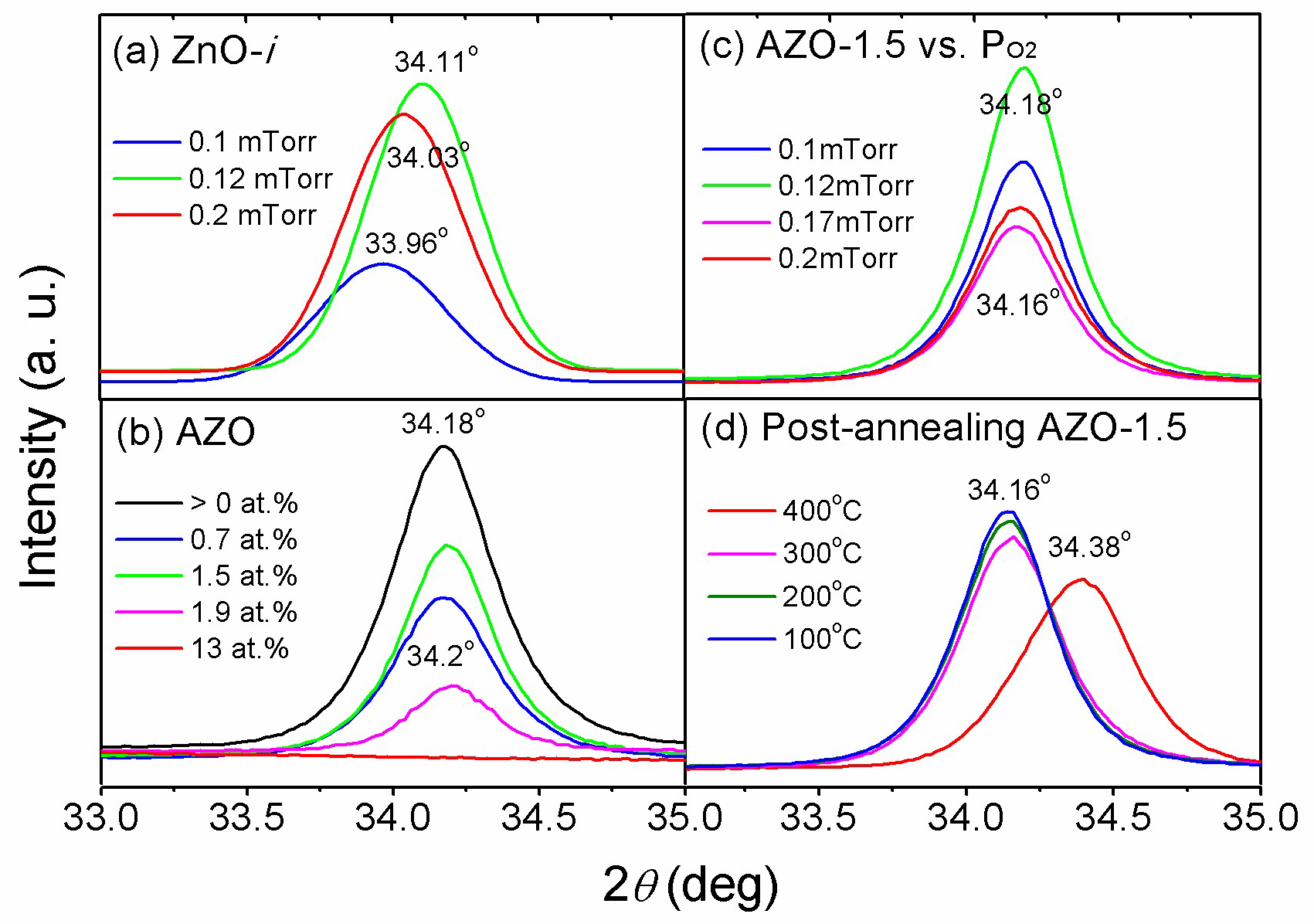
3.1. Deposition of Intrinsic ZnO Film

In our previous studies, we deposited intrinsic ZnO (ZnO-i) films with thicknesses of 92.6 ± 28.1 nm using ion-beam sputter deposition (IBSD) at room temperature under different oxygen partial pressure (PO₂). The deposition rate reduced with increasing PO₂ as a result of ZnO oxide formation on the surface of the metallic Zn target; the optimal PO₂ was found when the deposition rate no longer showed a clear decrease [30]. An optimal oxygen-deficient state was exhibited in the film deposited at PO₂ = 0.12 mTorr [15]. Moreover, the ZnO-i films deposited at PO₂ > 0.1 had an average transmittance superior to 80% in the visible and near-IR regions, with a transmittance close to zero in the UV range, as shown in Figure 3.
The average energy band gap (Eg) of the ZnO-i films, determined by applying the Tauc model in our previous study, is only 3.35 ± 0.045 eV [16]. The small 0.045-eV value appeared to be due to the insignificant blueshift in the optical band gap.
The ZnO-i film’s structures changed from the amorphous to the crystalline state, illustrating only the fitted X-ray diffraction (XRD) peak (002). In Figure 4a, the 2θ value (where θ is the Bragg diffraction angle) changes from 33.96° to 34.11° with increasing PO₂ when PO₂ > 0.1 mTorr, owing to the self-assembly property of the ZnO-i film [15,31]. The grain size mostly decreased with increasing PO₂ > 0.1 mTorr. The small variation of the ZnO-i grains is denoted by the gray triangles () in Figure 5. The film was optimally deposited at PO₂ = 0.12 mTorr and had the highest peak intensity and θ value. This film had a larger grain size of 17.9 nm, as evaluated by Scherrer’s formula s = 0.9λ/Bcosθ, where λ is the X-ray wavelength of 0.154 nm, s is the grain size, and B is the full width at half maximum (FWHM) of the XRD peak.
Otherwise, the average resistivity of the ZnO-i films was 6.3 ± 4.7 mΩ cm. The ZnO-i films deposited at PO₂ = 0.12 mTorr had a minimum resistivity of 2.40 ± 0.12 mΩ cm [15]. However, the resistivity of ZnO-i was still too large to apply to a CTO film for commercial use. The above-mentioned insignificant blueshift in the UV region and the high transmittance in the near-IR region were due to the low number of free carriers in the film.

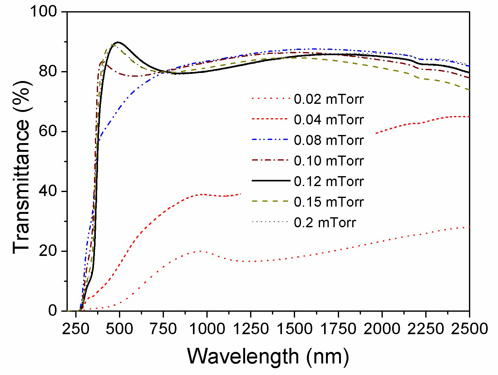
3.2. Deposition of AZO Films

The ZnO-i films exhibited n-type conductivity due to the intrinsic donors, oxygen vacancies, and/or Zn interstitials. They lacked thermal stability and had larger resistivity, although their crystallinities were improved and their resistivities were degraded by the post-annealing at high temperatures [32]. A method of extrinsically doping group III elements, such as Al, Ga, and In, which substitute the Zn sites, was introduced for the growth of n-type ZnO films to reduce the resistivity and improve the thermal stability of CTO films [33].
The Al dopants reacted more efficiently with oxygen compared to the Zn atoms during the growth or post-growth annealing, because the Gibbs free energy of −350.5 kJ/mol of the ZnO formation was larger than the −1582.3 kJ/mol of the Al2O3 formation [34]. The Al atoms substituted the Zn sites and became donors. The oxide, AlOx/Al2O3, inhibited the defects to affect the electrical and optical properties. Therefore, we deposited ZnO with different Al dopant concentrations (Al%) by using well-controlled ion-beam co-sputtering at different PO₂ and post-annealed the samples at different ambient temperatures for two hours.
Table 1 lists different Al% values for different H values for the sputtered areas of the Al target. AZO-0 had little Al content because the ion beam essentially individually sputtered the zinc target at H = 16.5 mm. The AZO film was prepared with an approximately 220 nm thickness at different H values. Although the ion beam equally co-sputtered the Al and Zn targets at H = 50 mm, the AZO-13 film was only doped with ~13 at.% Al concentration, since the sputtering rate of the Al metal was smaller than that of the Zn metal. The deposited film belongs to an amorphous film rather than a CTO film when the atomic percentage is greater than 13 at.%. We discuss successive alterations of the structural, electrical, and optical properties of the AZO films in the following section.

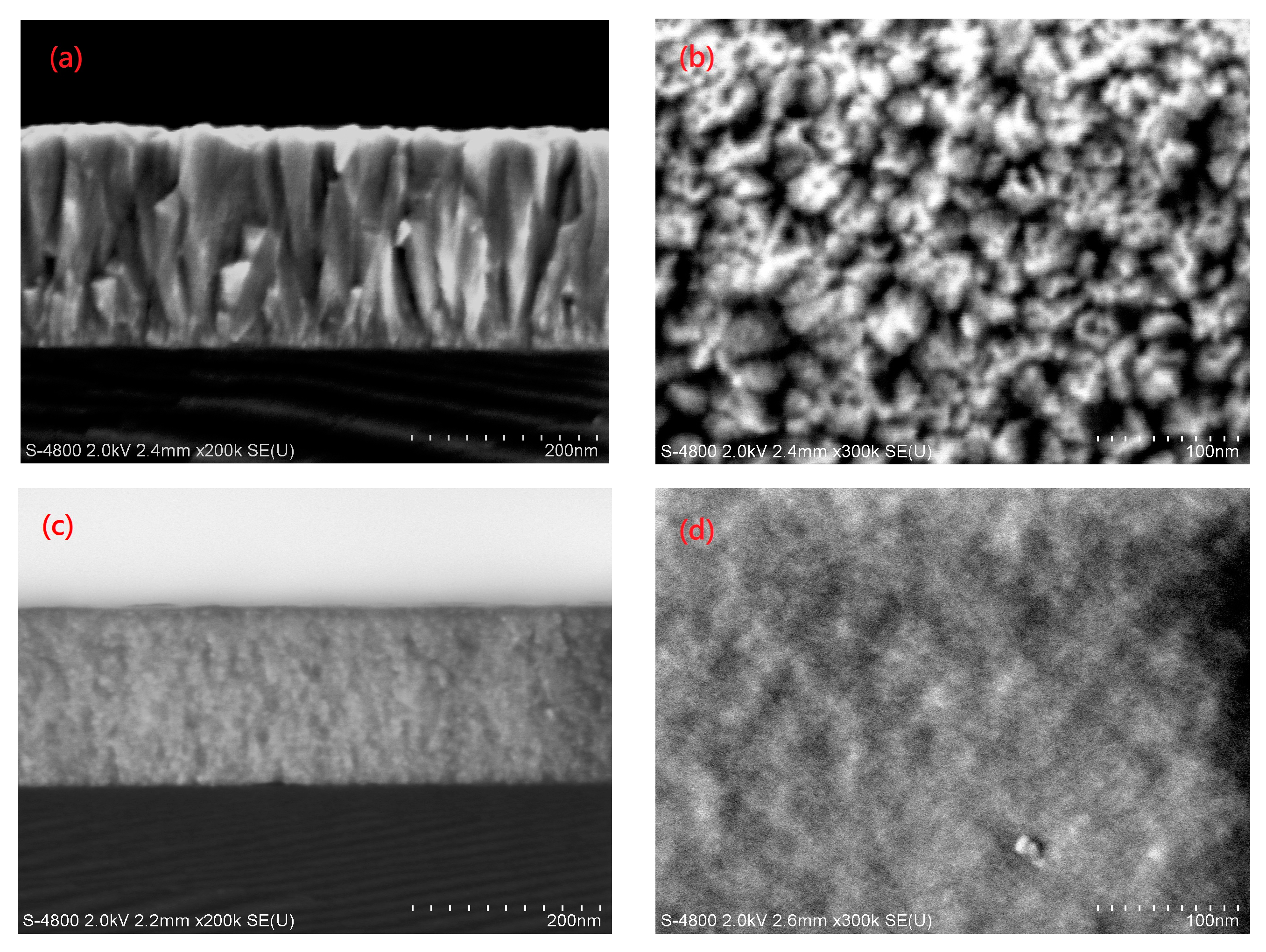
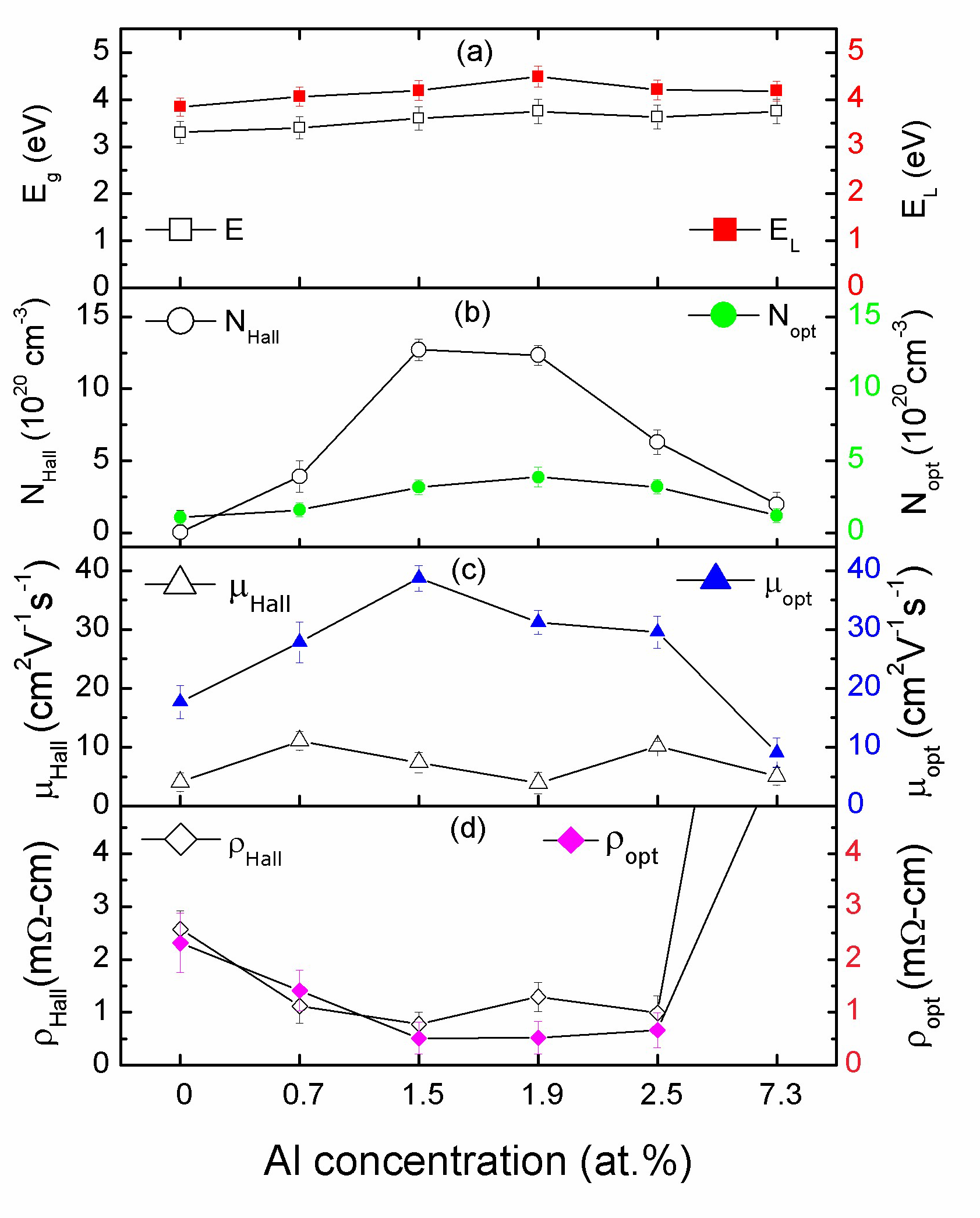
3.3. Structural Properties of the AZO Film

When Al3+ ion with a radius in the region of 53–67.5 pm replaced Zn2+ ion with a larger radius in the region of 74–104 pm, the diffraction angle θ became larger and the d-spacing between (002) atomic planes became shorter, owing to Bragg’s diffraction condition, d = λ/2sinθ. A suitable Al% was effective for releasing residual compressive stress in the plane of the AZO film, which is considered to be an effective way to improve film stability and increase grain size [19].
The AZO-0 XRD intensity was larger than that of the other AZO films, although the Al dopant inhibited the XRD intensity, as shown in Figure 4b. The crystal quality of the AZO films was degraded but they still exhibited a single-phase wurtzite ZnO structure. With increasing Al%, from >0 at.% to ~13 at.%, the value of 2θ shifting from 34.18° for the AZO-0 film to 34.2° for the AZO-13 film demonstrates that the Al–O bonds replaced the partial Zn–O bonds. As shown in Figure 5 with green circles () and in Table 1, the grain size apparently increased from 18.3, 18.7 to 22.9 nm, but the root-mean-square (RMS) value for the surface roughness reduced from 2.68, 2.54 to 2.48 nm with increasing Al%. When Al% increased to 2.5 at.%, the grain size decreased to 17.6 nm. Furthermore, the excess Al% eliminated the poly-crystalline XRD signal, resulting in a reduction in the RMS value to 1.02 nm for the AZO-13 film, as shown in Table 1. The pillar-like cross-section and the surface morphologies of the AZO samples, such as for AZO-0 to AZO-1.9, in the SEM images in Figure 6a,b illustrate the forms of the polycrystalline structure. The destruction of the amorphous structure of AZO-13 can be seen in Figure 6c,d.
The XRD peaks of the AZO-1.5 films deposited at different PO₂ values from 0.1 to 0.2 mTorr showed little change at approximately 34.18°, as shown in Figure 4c. The films deposited at 0.12 mTorr had the best poly-crystalline structure, owing to the high peak and the large grain of 20.9 nm, denoted with blue squares () in Figure 5. Moreover, the grain sizes, denoted with red diamonds () in Figure 5, were further reduced with increasing post-annealing ambient temperature, owing to the enhanced oxidation process.
The grain size affected the conductivity of the AZO film, as a result of the free-carrier scattering in the film. The larger the grain size, the smaller the resistivity. By controlling the deposition parameters, larger grain sizes could be grown in the AZO film. Although the grain size of the AZO-1.5 film was smaller than that of the AZO-1.9 film, the AZO-1.5 film had the optimal Al% by producing more free-carrier mobility to decrease the resistivity as discussed following section.

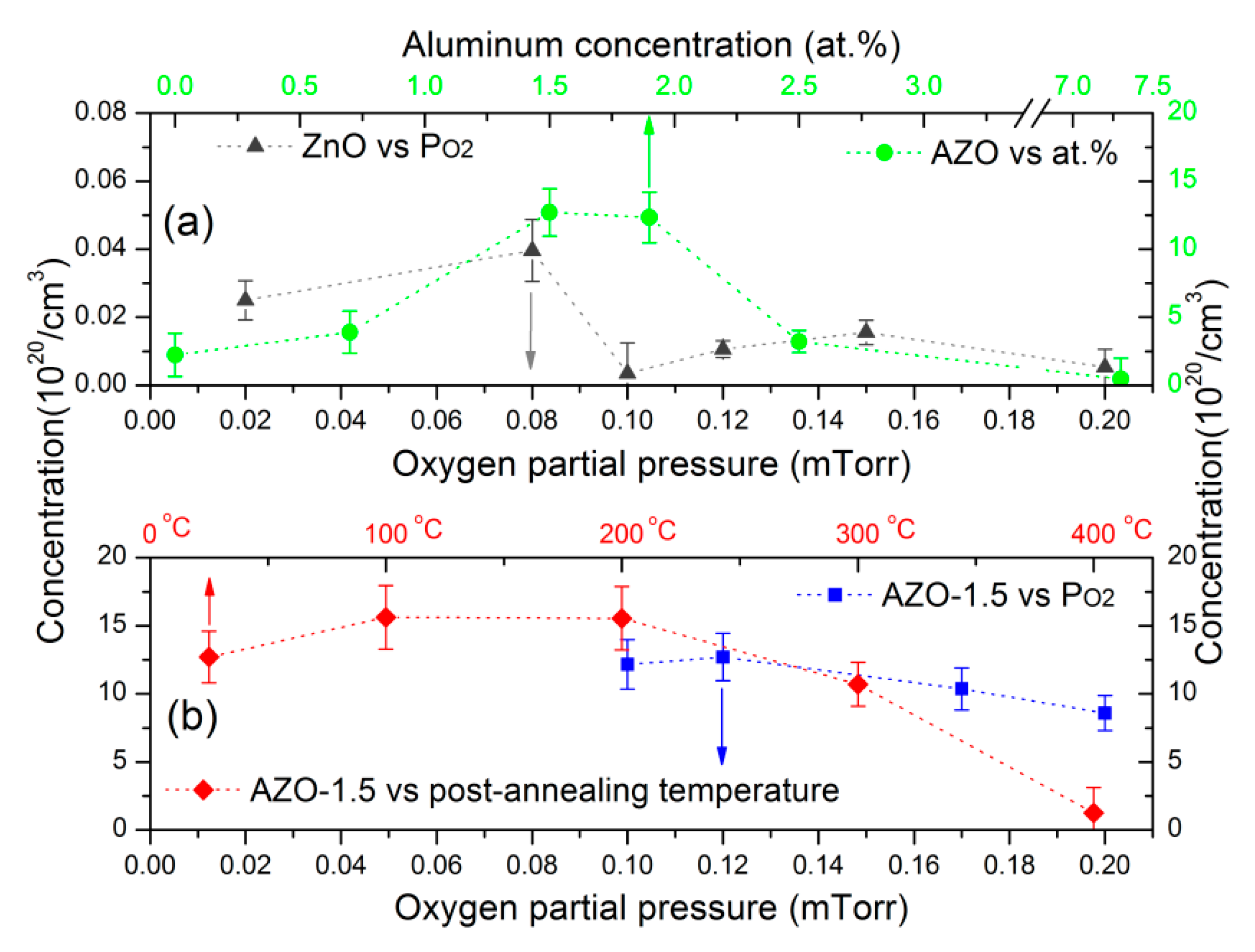
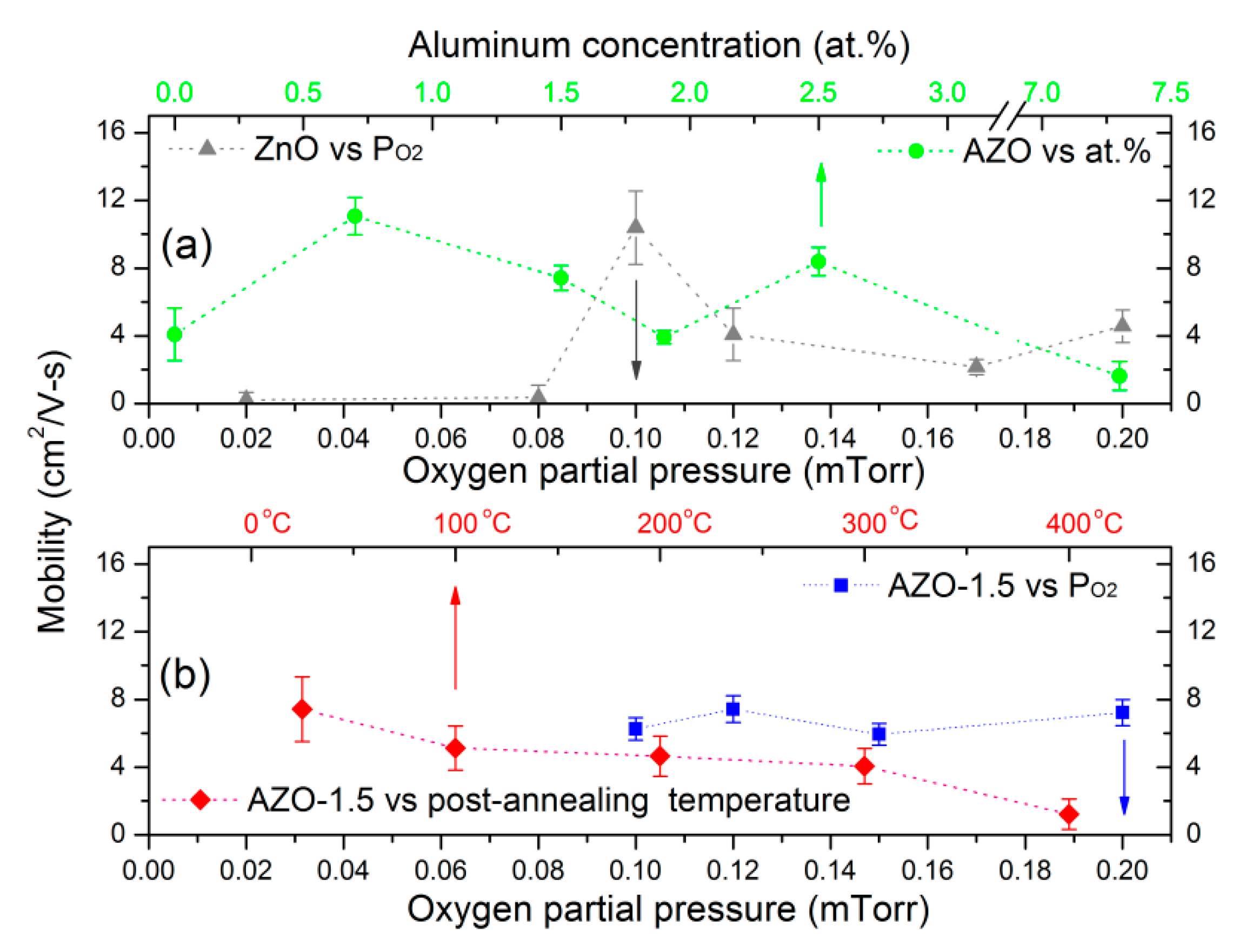
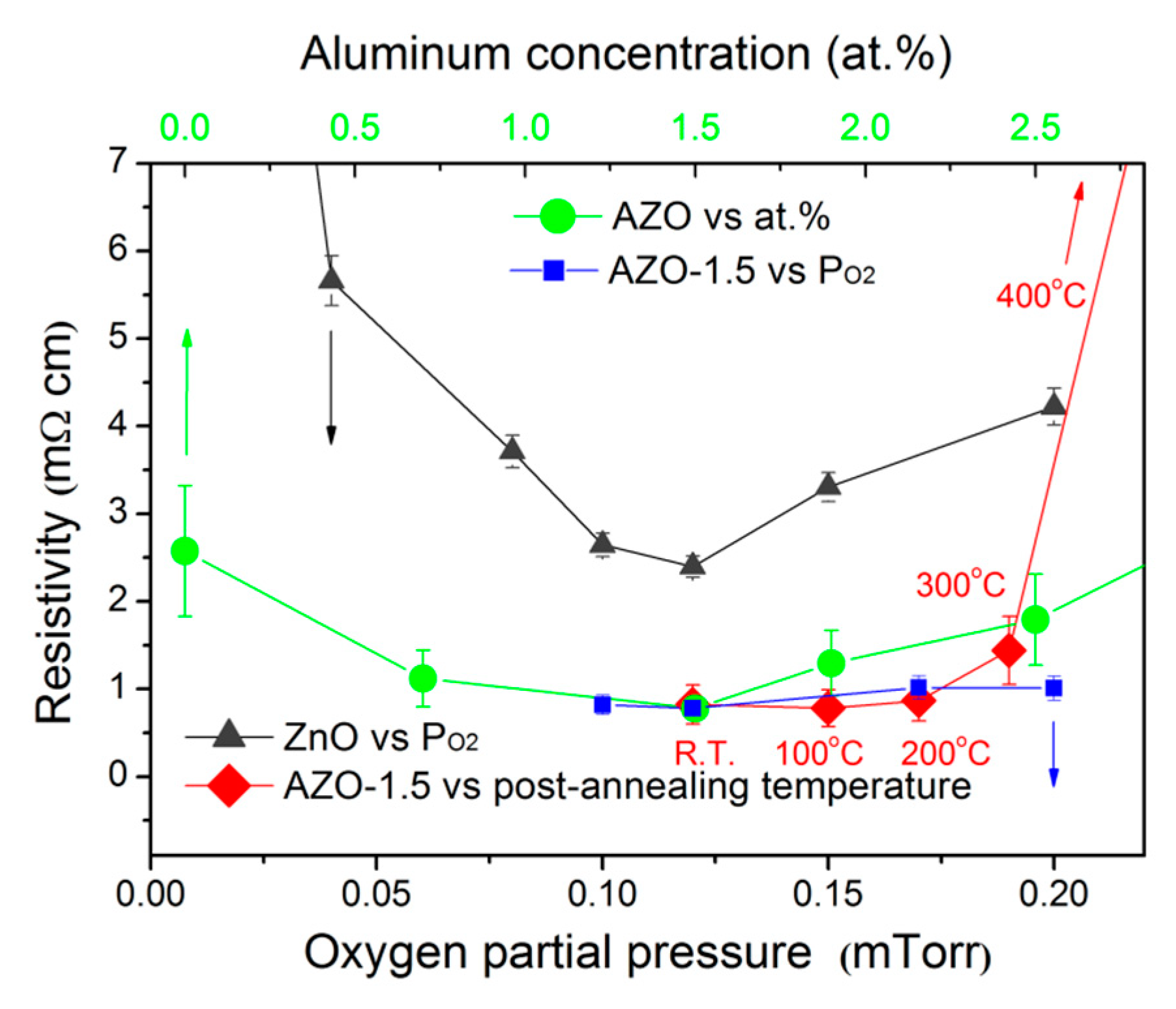
3.4. Electrical Properties

The conductive mechanism of the ZnO-i and AZO films was dominated by electrons produced from donor sites associated with oxygen vacancies, zinc interstitial sites, and antisite oxide in the film. In our studies, the n-type electron particles, obtained from the Hall-effect measurements, were the principal free carriers scattered in the polycrystalline films [19]. The relative concentration was influenced by the PO₂, Al%, and post-annealing temperatures in air, as shown in Figure 7.
However, the ZnO-i films deposited at various PO₂ had small n-type carrier concentrations, NHall < 0.05 × 1020 cm−3, as shown by the gray triangles () in Figure 7a. Although the NHall value decreased at PO₂ = 0.12 mTorr, the grain size and mobility values became significantly larger, as shown by the gray triangles () in Figure 8a. This improvement resulted from the formation of the ZnO crystalline structures deposited at this PO₂. Thus, the AZO-1.5 film’s NHall sharply increased to 14.36 × 1020 cm−3 and decreased in overall Al% to approximately 7.3 at.%, as shown by the green circles () in Figure 7a. The NHall values of the post-annealed films at 100 or 200 °C somewhat increased to 15.6 × 1020 cm−3, as shown by the red diamonds () in Figure 7b illustrating the AZO-1.5 film’s thermal stability. The AZO film became fully oxidized at post-annealing temperatures larger than 300 °C. In addition, the NHall value of the film deposited at PO₂ = 0.12 mTorr was somewhat larger than that of those deposited at other PO₂ values from 0.1 to 0.2 mTorr, as shown by the blue squares () in Figure 7b.
The free-carrier mobility was another important electrical issue for the CTO films. The ZnO-i mobility value increased at PO₂ = 0.1 mTorr, then decreased with increasing PO₂, as shown by the gray triangles () in Figure 8a, because the sub-oxide ZnO had more deficiencies than the full-oxide ZnO in the film. However, the selected PO₂ of 0.12 mTorr resulted in AZO film depositions that had larger grains as shown by the blue squares () in Figure 5, thus improving the mobility by reducing grain boundary scattering and increasing intra-grain scattering. Otherwise, increasing the PO₂ or the post-annealing temperature did not significantly improve the mobility, as shown by the blue squares () and red diamonds () in Figure 8b, respectively. The Al%, shown by the green circles () in Figure 8a, further altered the mobility of the free carriers, whose modification during the Hall measurements was relative to the mean free path L calculated using the formula [35]:
L = (3π2)1/3(he−2Hall−1NHall−2/3
The average L value of our AZO samples was 8.6 ± 2.1 nm [16]. However, the L values under the near-IR irradiation of a rapidly oscillating electric field in a small nanometer range were much smaller than the typical grain size [36]. Steinhauser et al. [28] studied the continuous transformation of grain boundary scattering to intra-grain scattering of boron-doped ZnO thin films, whose L values reduced from 3 × 10¹⁹ to 2 × 1020 cm−3 with increasing NHall. The intra-grain scattering mechanism occurred mainly when the L value was relatively shorter than the grain size of 600 nm, regardless of the grain boundary scattering, because the free carriers were transported easily inside the crystalline film [28]. However, in our research, an average grain size of only ~20 nm, much smaller than 600 nm, was a crucial factor for determining the scattering mechanism at NHall > 2 × 1020 cm−3. This disparity will be discussed again in Section 3.6.
The ZnO-i film’s resistivity varied with PO₂, as shown by the gray triangles () in Figure 9. The ZnO-i film deposited at PO₂ = 0.12 mTorr had the optimal smallest resistivity. Doping Al in the ZnO film was a good method to decrease the resistivity, ρHall, which initially decreased but then increased with increasing Al%. The AZO-1.5 film resistivity was the smallest, although its NHall was not the highest value, owing to the resistivity, in accordance with ρHall = 1/(NHallμHalle) [27], which changed very little at various PO₂ or at post-annealing temperatures of 100 °C and 200 °C in air. The poor thermal stability of the resistivity for the pure ZnO-i was improved but also reduced by the optimal extrinsic Al% of 1.5 at.% [33]. However, the NHall and μHall decreased and the ρHall increased with temperatures of up to 300 °C, as shown by Kuprenaite et al. [37].

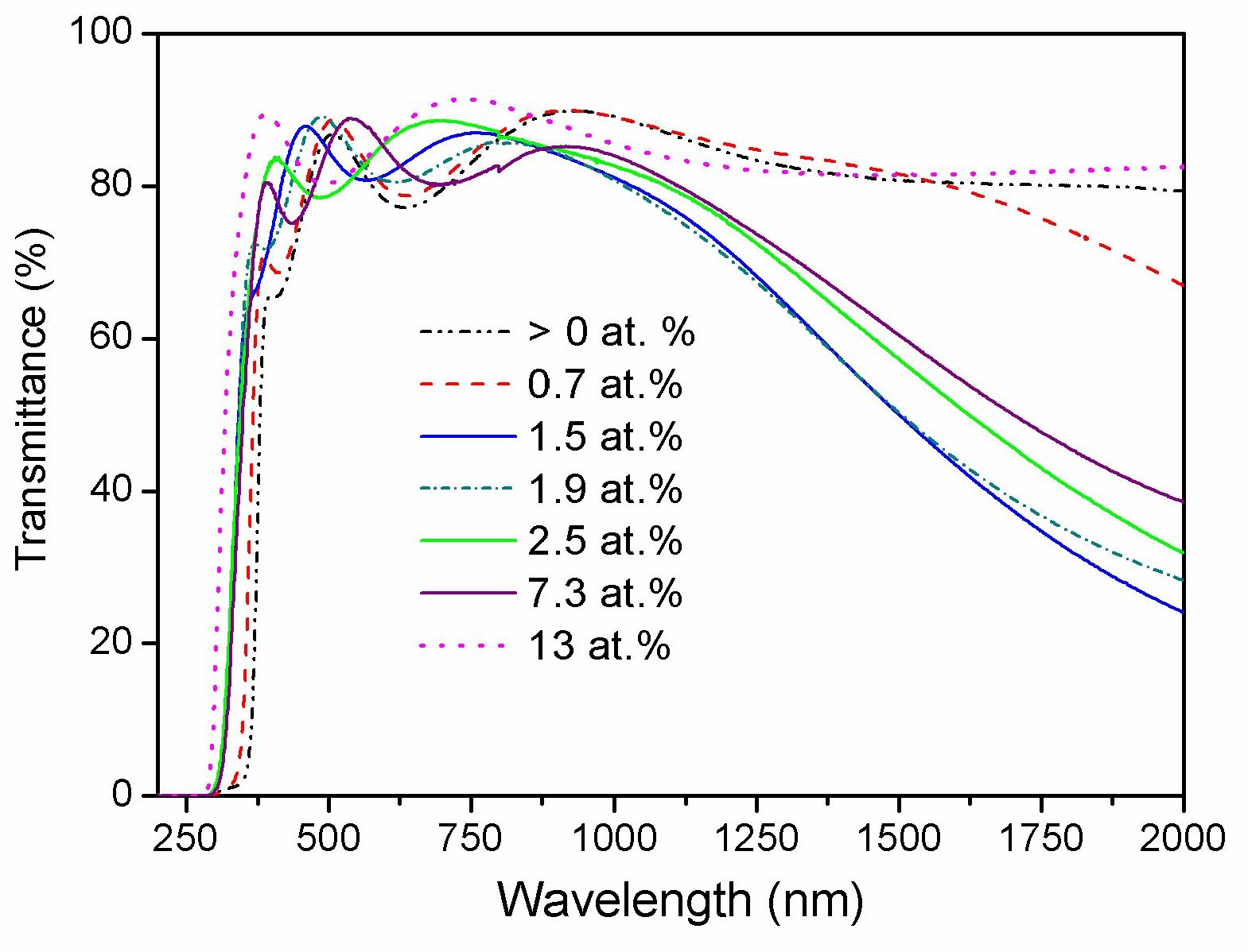
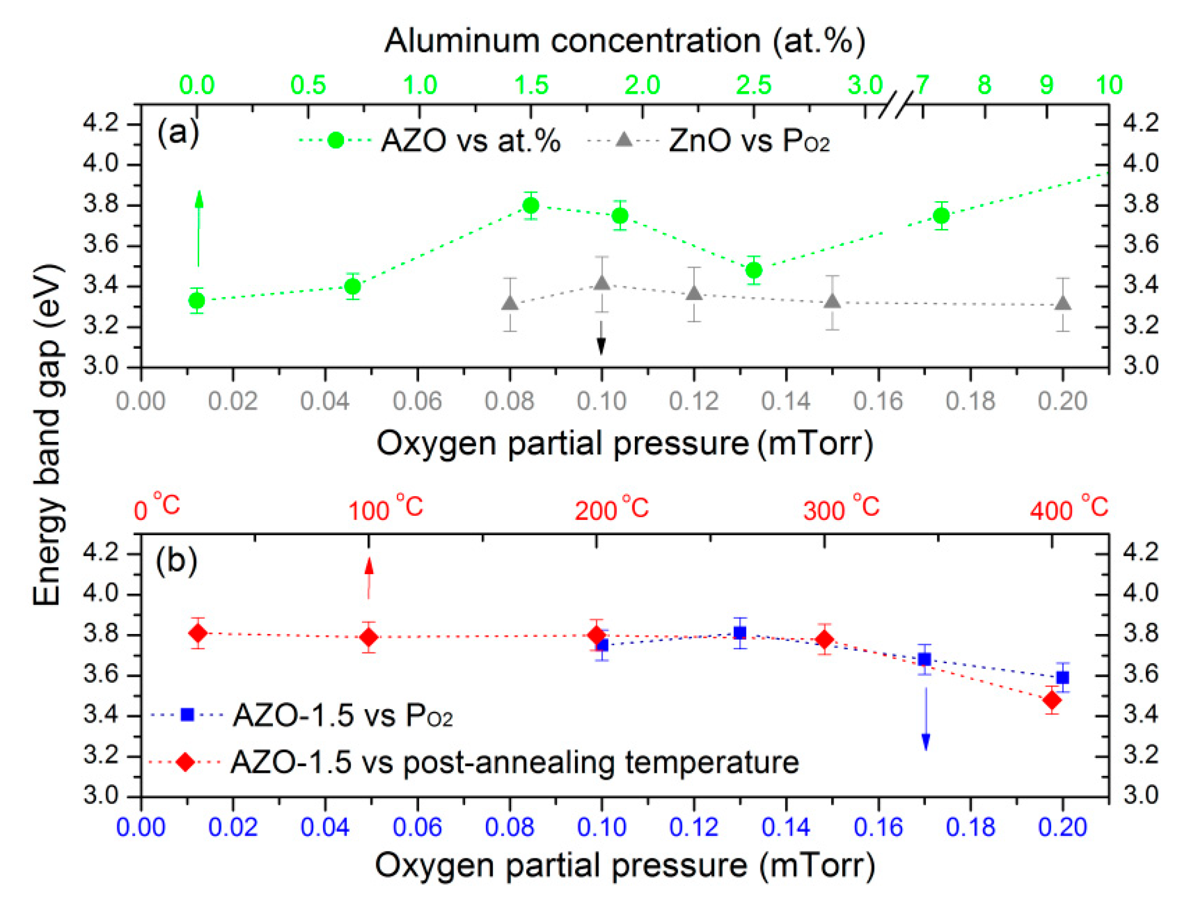
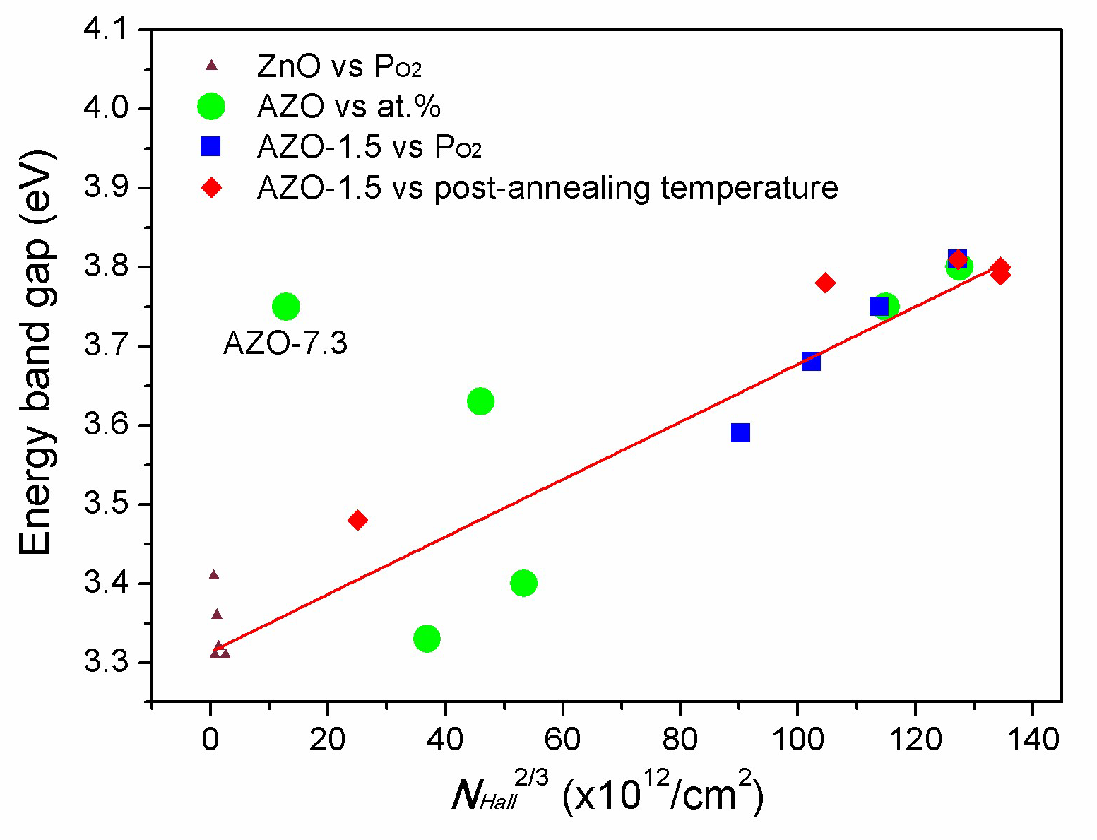
3.5. Optical Properties

The AZO film’s transmittance in the 250–2000 nm range is shown in Figure 10. The transmittance increases and decreases in the visible region as a result of optical interference. The average transmittance is superior to 80% in the visible range 400–700 nm and then decreases from 875 to 2000 nm, where the reflectance abruptly increases after the plasma wavelength; this phenomenon is related to the optical carrier concentration [12,28,38]. The dopant Al atoms that lost their valence electrons tended to form Al3+ cations more readily than the substituted Zn atoms, which tended to form Zn2+ cations. The valence electrons increased at the substituted Zn sites, resulting in the increase of the carrier concentration. The AZO-1.5 film at the lowest near-IR transmittance, shown in Figure 7a, had the greater number of free carriers. In contrast, for the AZO-13 film, there was no evident wurtzite ZnO in the film’s matrix, which contains hexagonal ZnO and rhombohedral Al2O3 structures in the heavy dopant, as found by Lu et al. [39]. It had a high near-IR transmittance due to the few free carriers. The AZO-7.3 film was partially composed of polycrystalline ZnO and AlOx/Al2O3 materials. We attribute the medium transmittance to the lower carrier concentration than that of ZnO-1.5 in the film. Thus, the near-IR transmittance, shown in Figure 10, decreased to the lowest value for the AZO-1.5 film then increased back to the highest value for the AZO-13 film with increasing Al%.
The optical absorption of the AZO films was close to zero at ~375 nm in the UV region. The Eg value, determined using the Tauc plot method, somewhat increased with increasing Al%. A small Eg redshift of the polycrystalline ZnO-i films deposited at PO₂ > 0.08 mTorr ranged from 3.41 to 3.31 eV, shown by the gray triangles () in Figure 11a. The redshift phenomenon was due to the ZnO-i structures changing from amorphous to polycrystalline structures [15,40]. In contrast, the Eg values of the AZO films for Al% 0, 0.7, and 1.5 at.%, with increasing NHall from 2.34 × 10²⁰, 3.9 × 10²⁰, and 12.7 × 1020 cm−3, as shown by the green circles () in Figure 7a, blueshifted from 3.3, 3.4, and 3.8 eV, as shown the green circles () in Figure 11a, respectively, due to the Burstein-Moss (B-M) effect [18,41] They redshifted again for Al% > 2.5 at.% for smaller values of NHall. The result agrees well with the observations from the optical and electrical measurements. Otherwise, the AZO-13 film, where the B-M effect was insignificant at NHall ≈ 0, still had a high Eg value of 4.2 eV because the film’s material consisted of Al2O3 with Eg of 6.2 eV and the amorphous ZnO with Eg of 3.4 eV [40].
In this study, the optical absorption in the UV region and the higher reflectance in the near-IR region are generally described as an extended Lorentz oscillator, including a Drude model, which will be discussed in Section 3.6.
Figure 11b shows that the AZO-1.5 film deposited at PO₂ = 0.12 mTorr had the largest Eg with the largest NHall due to the B-M effect, as shown by the blue squares () in Figure 7a. The Eg did not significantly change at post-annealing temperatures in air lower than 300 °C; however, it reduced significantly at 400 °C, due to an almost-full-oxidation of the film, as shown by the red diamonds () in Figure 7b.
Figure 12 shows the NHall2/3 values of the all ZnO-i and AZO films against Eg with a linear fitting. The B-M model describes the Eg of the AZO films with a variation of ΔEBM according to the formula:
E = E 0 + Δ E BM = 2 2 m * ( 3 π 2 N Hall ) 2 / 3
The ΔEBM value is the widening energy between the Eg of the AZO film and that of the AZO-0 film. The blueshift Eg resulted from the increasing NHall using Al-dopants. The ΔEBM was directly proportional to NHall2/3. The E0 value, obtained by extending the fitting line to the vertical axis in Figure 12, was approximately 3.3 eV, which agreed with the AZO-0 film value estimated from the transmittance in Figure 10. However, the AZO-7.3 film (green circles, ) did not lie on the fitting red line in Figure 10; we attribute this to the too low NHall in the film.

3.6. Spectroscopic Ellipsometry Study

We also illustrated the optical properties using an ellipsometry method for the low average mean square error (MSE) of 2.8 ± 0.5, which allowed for good simulations for the measured ellipsometry data and the fitting results of the films [24]. The average thickness was approximately 220 nm, as listed in Table 1. We assumed the EMA layer shown in Figure 2 to contain a mixture of voids and AZO material [18]. The average rough surface measured by an AFM was approximately 2.5 ± 0.7 nm. The six fitted coefficients of the AZO films are listed in Table 2.
The Eg, estimated using transmittance and shown by the white squares (□), and the gap energy EL, obtained using ellipsometry measurements and shown by the red squares (), were plotted against the Al% in Figure 13a. The Tauc plot is a common method for finding the Eg of crystalline semiconductors using Equation (10) for an indirect allowed transition:
αhν = A (hν − Eg)2
where α is the absorption coefficient calculated using α = 4πkw, hν is the photon energy, A is a constant, k is the extinction coefficient, and λw is the optical wavelength [42].
However, the average EL of the polycrystalline AZO film might be located at the center of the absorption band composed of the plural absorption bands. It was larger than the Eg from the Tauc plots, as determined by D’Elia et al. [26]. The absorption edge of the crystalline semiconductor abruptly terminated in this Eg region; however, due to the multiple absorption bands, the AZO polycrystalline structure extended beyond this region to EL.
The Nopt values, which was calculated using Equation (6) and the data in Table 2, and the NHall values both increased then decreased with increasing Al%, as shown in Figure 13b. The AZO-0.7 to AZO-2.5 films had the NHall > 2 × 1020 cm−3. The AZO-1.5 and AZO-1.9 films, which were approximately at the optimal doping level, had a larger difference between the NHall ~ 1.27 × 1021 cm−3 and Nopt ~3.1 × 1020 cm−3. Chinta et al. have also found the NHall value from 4.86 × 10¹⁹ to 2.99 × 1020 cm−3 and the Nopt value from 5.85 × 10¹⁹ to 2.29 × 1020 cm−3 for constant m* when the ZnO films were doped by Al from 0 to 10 at.% [43].
Figure 13c shows that the two μopt values calculated using Equation (7) and Table 2 were slightly lower because the free carriers scattered the charged donor impurity atoms more frequently under the electrostatic field. While the free carriers cross several grain boundaries, the scattering frequency ωGB is influenced by the grain boundary density [44]. By considering all scattering mechanisms, the total scattering frequency ωHall is the sum of the individual frequencies, which can be expressed by applying Matthiessen’s rule:
ωHall = ωGB + ωig
where ωig is the sum of the individual scattering frequencies for the ionized impurity scattering, neutral impurity scattering, and lattice vibration scattering mechanisms [45]. Since the mobility was inversely related to the scattering frequency, as shown in Equation (7), the reciprocal addition of the mobilities represents the Hall mobility μHall as:
μHall−1 = μig−1 + μGB−1
Although the intra-grain mobility μig was also limited by the grain size of approximately 20 nm in this study, the traveling distance of approximately a few nanometers, where the electron interacted with photons due to the application of a rapidly oscillating electromagnetic field, was much smaller than the grain size. The depleted scattering region at the boundaries occupied only a small volume compared with the grain size. Hence, the mobility μopt was equal to the intra-grain mobility μig, neglecting the grain boundary scattering [45]. To observe the discrepancy between μopt and μHall, Equation (13) is rewritten as:
μoptGB = (μopt − μHall)/μHall = μoptHall − 1
In this study, for light doping (e.g., the AZO-0 film) or over doping (e.g., the AZO-7.3 film) the NHall < 2 × 1020 cm−3 and the difference between Nopt and NHall were smaller. The greatest difference in terms of the two free carrier densities occurred for the AZO-1.5 film, as shown in Figure 13b. The discrepancy between μopt and μHall was simultaneously larger than that for the others, as shown in Figure 13c. The μopt value of ~38 cm2 V−1 s−1 was much larger than the μHall value of ~8 cm2 V−1 s−1. Knoops et al. also studied the μopt and μHall values of the deposited 150-nm-thickness AZO film were approximately 17 and 12 cm2 V−1 s−1, respectively [46]. Such inequality has also been reported for boron-doped ZnO film, owing to its microstructure with a poorly conducting grain boundary [28]. In this work, the grain boundary was caused by the small grain size of ~20 nm in the AZO film. From Equation (14), the grain boundary scattering effect was predominant for the larger μoptGB values that had the highest μopt and the lower μHall, as shown in Figure 13c.
The AZO-1.5 film also showed the lowest ρopt. The ρopt values, which were calculated with Equation (8) and the data in Table 2, and the measured ρHall values simultaneously decreased then increased with Al% increasing from 0, 1.5, to 7.3 at.%, as shown by the pink diamonds () in Figure 13d. The AZO-7.3 film had the larger resistivity, owing to the Al2O3 formation, as shown by the XPS spectra shown in Figure 14 for selected samples. The spectral areas for AlOx, for the AlߝOߝZn bonding, and Al2O3, for the amorphous structure, increased with increasing Al%. The excess of Al atoms containing oxygen vacancies in the film may separate into grain boundaries and easily form a neutral Al2O3-based defect complex, which did not contribute to free electrons and acted as scattering centers, thereby deteriorating the electrical properties [47]. That is, the larger Al2O3 area for the AZO-7.3 film was observed in the Al 2p XPS spectra.
The ρopt and ρHall were almost identical in Figure 13b,c at each Al%, despite the above-mentioned observations that NHall > Nopt and μHall < μopt, because the resistivity was mainly proportional to the reciprocal products of the mobilities and the free carrier densities. Moreover, the AZO-1.5 film had the smallest resistivities of ρopt = 0.51 mΩ cm and ρHall = 0.78 mΩ cm.
The optical properties of the AZO films were affected by many factors, such as the polycrystalline structure, surface morphology, optical absorption, and Al%. The Al dopant in the AZO film destroyed the ZnO wurtzite structure because the Al-O bonds replaced the Zn-O bonds and shrank the bond length. The higher the Al%, the greater the grain size for Al% < 1.9 at.%, as shown by the green circles () in Figure 5. Volintiru et al. also investigated the optical properties affected by the two film’s pyramid- and pillar-like growth structures. The optical interference reduced the pyramid-like structure, owing to the optical scattering on the rough surface and the large grain boundary of the film [12]. In our study, the AZO films were between pyramid- and pillar-like grains, as shown in Figure 6a,b. Grain sizes of approximately 20 nm were greater than those of the pillar-like structure. Moreover, ion-beam-sputtering films have a small surface roughness, low extinction coefficient, and high packing density [30,48]. Therefore, these films have less multi-reflection of light scattering between the polycrystalline boundaries. The transmittance of the apparent interference phenomenon varied with different wavelengths in the visible range, as shown in Figure 10. Moreover, the near-IR transmittance reduction resulted from the increase in the higher k-value due to the transmittance T in the air, which can be expressed as [49]:
T = 4 n ( 1 + n ) 2 + k 2
The k values in the visible range were smaller than those in the UV range due to the optical absorption and in the near-IR range due to the high free-carrier density. Such as, the optimal doping AZO-1.5 film had the smallest transmittance in the near-IR region due to the great k value. For another limitation, the heavily doping AZO-13 film had a steady high transmittance because it is almost fully oxidized. Its k value was smaller in the near-IR region.

4. Conclusions

The ZnO film deposited at oxygen partial pressure PO₂ = 0.12 mTorr had the smallest resistivity, of approximately 2.5 mΩ. The film’s resistivity was reduced and its thermal stability was improved, at post-annealing temperatures of 100 or 200 °C in air, by using ion-beam co-sputtering for two Al and Zn targets. The optimal extrinsic Al dopant concentration (Al%) of 1.5 at.% allows the Al-doped ZnO (AZO) film to have a high transmittance of >80% in the visible regions, a grain size of approximately 20 nm with high crystalline orientation (002), and the smallest and thermally stable resistivity of 7.8 × 10⁻⁴ Ω cm.
Moreover, AZO thin films deposited with various Al% values from 0 to 13 at.% were prepared. We used an ellipsometry model with two Lorentz oscillators to successfully analyze each film’s electrical and optical properties. The various Nopt, μopt, and ρopt electrical properties were compared to the NHall, μHall, and ρHall values measured using the Hall effect. For the optimal AZO-1.5% film sample, Nopt = 3.1 × 1020 cm−3 < NHall = 1.27 × 1021 cm−3 and μopt = 38 cm2 V−1 s−1 > μHall = 7.5 cm2 V−1 s−1, due to the mechanism limiting the electron mobility. This mechanism is determined by the grain boundary scattering for the smaller grain size in our study. Each film’s optical properties were evaluated to obtain the optical absorption in the UV region and the low transmittance in the near-IR region.

Author Contributions

Conceptualization, J.-C.H.; Data Curation, Y.-Y.C.; Formal Analysis, J.-C.H.; Funding Acquisition, J.-C.H.; Investigation, Y.-Y.C.; Methodology, J.-C.H.; Project Administration, J.-C.H.; Resources, J.-C.H.; Software, J.-C.H. and Y.-Y.C.; Supervision, J.-C.H.; Validation, J.-C.H. and Y.-Y.C.; Visualization, J.-C.H.; Writing–Original Draft Preparation, J.-C.H.; Writing–Review & Editing, J.-C.H.

Funding

This research was funded by the Ministry of Science and Technology of Taiwan (No. MOST 105-2221-E-030-007-MY3 and MOST 106-2112-M-030-001-MY2).

Conflicts of Interest

The authors declare no conflict of interest.

References

  1. Jiang, X.; Jia, C.L.; Szyszka, B. Manufacture of specific structure of aluminum-doped zinc oxide films by patterning the substrate surface. Appl. Phys. Lett. 2002, 80, 3090. [Google Scholar] [CrossRef]
  2. Kohan, A.F.; Ceder, G.; Morgan, D.; Van De Walle, C.G. First-principles study of native point defects in ZnO. Phys. Rev. B 2000, 61, 15019. [Google Scholar] [CrossRef]
  3. Kayaci, F.; Vempati, S.; Donmez, I.; Biyikli, N.; Uyar, T. Role of zinc interstitials and oxygen vacancies of ZnO in photocatalysis: A bottom-up approach to control defect density. Nanoscale 2014, 6, 10224–10234. [Google Scholar] [CrossRef] [PubMed]
  4. Takata, S.; Minami, T.; Nanto, H. The stability of aluminium-doped ZnO transparent electrodes fabricated by sputtering. Thin Solid Films 1986, 135, 183–187. [Google Scholar] [CrossRef]
  5. Minami, T. New n-type transparent conducting oxides. MRS Bull. 2000, 25, 38–44. [Google Scholar] [CrossRef]
  6. T-Thienprasert, J.; Rujirawat, S.; Klysubun, W.; Duenow, J.N.; Coutts, T.J.; Zhang, S.B.; Look, D.C.; Limpijumnong, S. Compensation in Al-doped ZnO by Al-related acceptor complexes: Synchrotron X-ray absorption spectroscopy and theory. Phys. Rev. Lett. 2013, 110, 055502. [Google Scholar] [CrossRef]
  7. Verma, A.; Khan, F.; Kumar, D.; Kar, M.; Chakravarty, B.C.; Singh, S.N.; Husain, M. Sol-gel derived aluminum doped zinc oxide for application as anti-reflection coating in terrestrial silicon solar cells. Thin Solid Films 2010, 518, 2649–2653. [Google Scholar] [CrossRef]
  8. Budianu, E.; Purica, M.; Iacomi, F.; Baban, C.; Prepelita, P.; Manea, E. Silicon metal-semiconductor-metal photodetector with zinc oxide transparent conducting electrodes. Thin Solid Films 2008, 516, 1629–1633. [Google Scholar] [CrossRef]
  9. Chiang, Y.-F.; Sung, C.-C.; Ro, R. Effects of metal buffer layer on characteristics of surface acoustic waves in ZnO/metal/diamond structures. Appl. Phys. Lett. 2010, 96, 154104. [Google Scholar] [CrossRef]
  10. Jeong, S.S.; Mittiga, A.; Salza, E.; Masci, A.; Passerini, S. Electrodeposited ZnO/Cu2O heterojunction solar cells. Electrochim. Acta 2008, 53, 2226–2231. [Google Scholar] [CrossRef]
  11. Yu, K.M.; Mayer, M.A.; Speaks, D.T.; He, H.; Zhao, R.; Hsu, L.; Mao, S.S.; Haller, E.E.; Walukiewicz, W. Ideal transparent conductors for full spectrum photovoltaics. J. Appl. Phys. 2012, 111, 123505. [Google Scholar] [CrossRef]
  12. Volintiru, I.; Creatore, M.; Van De Sanden, M.C.M. In situ spectroscopic ellipsometry growth studies on the Al-doped ZnO films deposited by remote plasma-enhanced metalorganic chemical vapor deposition. J. Appl. Phys. 2008, 103, 033704. [Google Scholar] [CrossRef] [Green Version]
  13. Lin, K.M.; Lee, Y.H.; Huang, W.Y.; Hsieh, C.T.; Hsu, C.K. Spectroscopic ellipsometry study on strain evolution of transparent conductive thin films prepared by RF sputtering method. Adv. Mater. Res. 2015, 1110, 222–225. [Google Scholar] [CrossRef]
  14. Kinsey, N.; Devault, C.; Kim, J.; Ferrera, M.; Shalaev, V.M.; Boltasseva, A. Epsilon-near-zero Al-doped ZnO for ultrafast switching at telecom wavelengths. Optica 2015, 2, 616–622. [Google Scholar] [CrossRef]
  15. Hsu, J.-C.; Chiang, Y.-S. Influence of oxygen on zinc oxide films fabricated by ion-beam sputter deposition. ISRN Mater. Sci. 2013, 2013, 710798. [Google Scholar] [CrossRef]
  16. Chen, Y.-Y.; Hsu, J.-C.; Wang, P.W.; Pai, Y.-W.; Wu, C.-Y.; Lin, Y.-H. Dependence of resistivity on structure and composition of AZO films fabricated by ion beam co-sputtering deposition. Appl. Surf. Sci. 2011, 257, 3446–3450. [Google Scholar] [CrossRef]
  17. Chen, Y.-Y.; Hsu, J.-C.; Lee, C.-Y.; Wang, P.W. Influence of oxygen partial pressure on structural, electrical, and optical properties of Al-doped ZnO film prepared by the ion beam co-sputtering method. J. Mater. Sci. 2013, 48, 1225–1230. [Google Scholar] [CrossRef]
  18. Hsu, J.-C.; Lin, Y.-H.; Wang, P.W.; Chen, Y.-Y. Spectroscopic ellipsometry studies on various zinc oxide films deposited by ion beam sputtering at room temperature. Appl. Opt. 2012, 51, 1209–1215. [Google Scholar] [CrossRef]
  19. Chen, Y.-Y.; Wang, P.W.; Hsu, J.-C.; Lee, C.-Y. Post-annealing properties of aluminum-doped zinc oxide films fabricated by ion beam co-sputtering. Vacuum 2013, 87, 227–231. [Google Scholar] [CrossRef]
  20. Woollam, J.A.; Bungay, C.L.; Tiwald, T.E.; Liphardt, M.M.; Synowicki, R.A.; Pribil, G.K.; Herzinger, C.M.; Johs, B.D.; Hilfiker, J.N. Sample Analysis Methodology Utilizing Electromagnetic Radiation. U.S. Patent No. 7,385,697, 10 June 2008. [Google Scholar]
  21. Gong, L.; Ye, Z.; Lu, J.; Zhu, L.; Huang, J.; Gu, X.; Zhao, B. Highly transparent conductive and near-infrared reflective ZnO:Al thin films. Vacuum 2010, 84, 947–952. [Google Scholar] [CrossRef]
  22. Kim, H.; Gilmore, C.M.; Pique, A.; Horwitz, J.S.; Mattoussi, H.; Murata, H.; Kafafi, Z.H.; Chrisey, D.B. Electrical, optical, and structural properties of indium–tin–oxide thin films for organic light-emitting devices. J. Appl. Phys. 1999, 86, 6451. [Google Scholar] [CrossRef]
  23. Aspnes, D.E.; Theeten, J.B.; Hottier, F. Investigation of effective-medium models of microscopic surface roughness by spectroscopic ellipsometry. Phys. Rev. B 1979, 20, 3292. [Google Scholar] [CrossRef]
  24. Fujiwara, H. Spectroscopic Ellipsometry: Principles and Applications; John Wiley & Sons: Hoboken, NJ, USA, 2007. [Google Scholar]
  25. Tseng, K.-S.; Lo, Y.-L. Investigation into inhomogeneous electrical and optical properties of indium tin oxide film using spectroscopic ellipsometry with multi-layer optical models. Opt. Mater. Express 2014, 4, 43–56. [Google Scholar] [CrossRef]
  26. D’Elia, S.; Scaramuzza, N.; Ciuchi, F.; Versace, C.; Strangi, G.; Bartolino, R. Ellipsometry investigation of the effects of annealing temperature on the optical properties of indium tin oxide thin films studied by Drude–Lorentz model. Appl. Surf. Sci. 2009, 255, 7203–7211. [Google Scholar] [CrossRef]
  27. Hamberg, I.; Granqvist, C.G. Evaporated Sn-doped In2O3 films: Basic optical properties and applications to energy-efficient windows. J. Appl. Phys. 1986, 60, R123. [Google Scholar] [CrossRef]
  28. Steinhauser, J.; Faÿ, S.; Oliveira, N.; Vallat-Sauvain, E.; Ballif, C. Transition between grain boundary and intragrain scattering transport mechanisms in boron-doped zinc oxide thin films. Appl. Phys. Lett. 2007, 90, 142107. [Google Scholar] [CrossRef] [Green Version]
  29. Tahar, R.B.H.; Ban, T.; Ohya, Y.; Takahashi, Y. Tin doped indium oxide thin films: Electrical properties. J. Appl. Phys. 1998, 83, 2631. [Google Scholar] [CrossRef]
  30. Hsu, J.-C.; Lee, C.-C. Single- and dual-ion-beam sputter deposition of titanium oxide films. Appl. Opt. 1998, 37, 1171–1176. [Google Scholar] [CrossRef]
  31. Jiang, Y.; Bahlawane, N. Effect of nucleation and growth kinetics on the electrical and optical properties of undoped ZnO films. J. Phys. Chem. C 2010, 114, 5121–5125. [Google Scholar] [CrossRef]
  32. Minami, T.; Hanato, H.; Shooji, S.; Takata, S. The stability of zinc oxide transparent electrodes fabricated by RF magnetron sputtering. Thin Solid Films 1984, 111, 167–174. [Google Scholar] [CrossRef]
  33. Haug, F.-J.; Geller, Z.; Zogg, H.; Tiwari, A.N.; Vignali, C. Influence of deposition conditions on the thermal stability of ZnO:Al films grown by RF magnetron sputtering. J. Vac. Sci. Technol. A 2001, 19, 171. [Google Scholar] [CrossRef]
  34. Kim, K.-K.; Tampo, H.; Song, J.-O.; Seong, T.-Y.; Park, S.-J.; Lee, J.-M.; Kim, S.-W.; Fujita, S.; Niki, S. Effect of rapid thermal annealing on Al doped n-ZnO films grown by RF-magnetron sputtering. Jpn. J. Appl. Phys. 2005, 44, 4776–4779. [Google Scholar] [CrossRef]
  35. Kittel, C. Introduction to Solid State Physics, 5th ed.; Wiley: Hoboken, NJ, USA, 1976. [Google Scholar]
  36. Guglielmi, M.; Menegazzo, E.; Paolizzi, M.; Gasparro, G.; Ganz, D.; Pütz, J.; Aegerter, M.A.; Hubert-Pfalzgraf, L.; Pascual, C.; Durán, A.; et al. Sol-gel deposited Sb-doped tin oxide films. J. Sol-Gel Sci. Technol. 1998, 13, 679–683. [Google Scholar] [CrossRef]
  37. Kuprenaite, S.; Abrutis, A.; Kubilius, V.; Murauskas, T.; Saltyte, Z.; Plausinaitiene, V. Effects of annealing conditions and film thickness on electrical and optical properties of epitaxial Al-doped ZnO films. Thin Solid Films 2016, 599, 19–26. [Google Scholar] [CrossRef]
  38. Singh, A.V.; Mehra, R.M.; Buthrath, N.; Wakahara, A.; Yoshida, A. Highly conductive and transparent aluminum-doped zinc oxide thin films prepared by pulsed laser deposition in oxygen ambient. J. Appl. Phys. 2001, 90, 5661. [Google Scholar] [CrossRef]
  39. Lu, J.; Ye, Z.; Zeng, Y.; Zhu, L.; Wang, L.; Yuan, J.; Zhao, B.; Liang, Q. Structural, optical, and electrical properties of (Zn,Al)O films over a wide range of compositions. J. Appl. Phys. 2006, 100, 073714. [Google Scholar] [CrossRef]
  40. Tan, S.T.; Chen, B.J.; Sun, X.W.; Fan, W.J.; Kwok, H.S.; Zhang, X.H.; Chua, S.J. Blueshift of optical band gap in ZnO thin films grown by metal-organic chemical-vapor deposition. J. Appl. Phys. 2005, 98, 013505. [Google Scholar] [CrossRef]
  41. Sernelins, B.E.; Berggren, K.-F.; Jin, Z.-C.; Hamberg, I.; Granqvist, C.G. Band-gap tailoring of ZnO by means of heavy Al doping. Phys. Rev. B 1988, 37, 10244. [Google Scholar] [CrossRef]
  42. Tauc, J.; Grigorovici, R.; Vancu, A. Optical properties and electronic structure of amorphous germanium. Phys. Status Solidi B 1966, 15, 627–637. [Google Scholar] [CrossRef]
  43. Chinta, P.V.; Lozano, O.; Wadekar, P.V.; Hsieh, W.C.; Seo, H.W.; Yeh, S.W.; Liao, C.H.; Tu, L.W.; Ho, N.J.; Zhang, Y.S.; et al. Evolution of metallic conductivity in epitaxial ZnO thin films on systematic Al doping. J. Electron. Mater. 2017, 46, 2030–2039. [Google Scholar] [CrossRef]
  44. Yamada, T.; Makino, H.; Yamamoto, N.; Yamamoto, T. Ingrain and grain boundary scattering effects on electron mobility of transparent conducting polycrystalline Ga-doped ZnO films. J. Appl. Phys. 2010, 107, 123534. [Google Scholar] [CrossRef]
  45. Nomoto, J.; Makino, H.; Yamamoto, T. Carrier mobility of highly transparent conductive Al-doped ZnO polycrystalline films deposited by radio-frequency, direct-current, and radio-frequency-superimposed direct-current magnetron sputtering: Grain boundary effect and scattering in the grain bulk. J Appl. Phys. 2015, 117, 045304. [Google Scholar] [CrossRef]
  46. Knoops, H.C.M.; Van De Loo, B.W.H.; Smit, S.; Ponomarev, M.V.; Weber, J.-W.; Sharma, K.; Kessels, W.M.M.; Creatore, M. Optical modeling of plasma-deposited ZnO films: Electron scattering at different length scales. J. Vac. Sci. Technol. A 2015, 33, 021509. [Google Scholar] [CrossRef] [Green Version]
  47. Pei, Z.; Zhang, X.; Zhang, G.; Gong, J.; Sun, C.; Huang, R.; Wen, L. Transparent conductive ZnO:Al thin films deposited on flexible substrates prepared by direct current magnetron sputtering. Thin Solid Films 2006, 497, 20–23. [Google Scholar] [CrossRef]
  48. Lee, C.-C.; Hsu, J.-C.; Wong, D.-H. The characteristics of some metallic oxides prepared in high vacuum by ion beam sputtering. Appl. Surf. Sci. 2001, 171, 151–156. [Google Scholar] [CrossRef]
  49. Macleod, H.A. Thin-Film Optical Filter, 4th ed.; CRC Press: Boca Raton, FL, USA, 2010. [Google Scholar]
Figure 1. Schematic of the ion-beam co-sputtering system used in this study.
Coatings 09 00004 g001
Figure 2. Al-doped ZnO (AZO) layer ellipsometry model using two Lorentz oscillators. The surface roughness is simulated using an effective medium approximation (EMA) layer consisting of the transition layer and voids.
Coatings 09 00004 g002
Figure 3. Transmittances of pure ZnO films deposited using ion-beam sputter deposition (IBSD) at various oxygen partial pressures (PO₂).
Coatings 09 00004 g003
Figure 4. XRD patterns obtained for (a) ZnO-i films deposited at various PO₂, (b) AZO films doped at various Al%, (c) AZO-1.5 films deposited at various PO₂, and (d) AZO-1.5 films at various post-annealing temperatures in air.
Coatings 09 00004 g004
Figure 5. XRD grain sizes of ZnO-i films deposited at various PO₂ (gray triangles ), AZO films at various PO₂ (blue squares ), AZO films doped at various Al concentrations (green circles ), and AZO films at various post-annealing temperatures in air (red diamonds ).
Coatings 09 00004 g005
Figure 6. SEM morphologies of the (a) surface and (b) cross-section of the AZO-1.5 film; SEM morphologies of the (c) surface and (d) cross-section of the AZO-13 film.
Coatings 09 00004 g006
Figure 7. (a) Free-carrier concentrations of ZnO films prepared at different oxygen pressures and doped Al concentrations; (b) Free-carrier concentrations of AZO-1.5 films prepared at different oxygen pressures and post-annealing at different temperatures in air.
Coatings 09 00004 g007
Figure 8. (a) Free-carrier mobilities of ZnO films prepared at different oxygen pressures and doped Al concentrations; (b) Free-carrier mobilities of AZO-1.5 films prepared at different oxygen pressures and post-annealing at different temperatures in air.
Coatings 09 00004 g008
Figure 9. The resistivity of ZnO films deposited at various oxygen partial pressures.
Coatings 09 00004 g009
Figure 10. Transmittance spectra of AZO films doped with different concentrations of aluminum (at.%).
Coatings 09 00004 g010
Figure 11. (a) Energy band gaps of ZnO films prepared at different oxygen pressures and doped Al concentrations; (b) Energy band gaps of AZO-1.5 films prepared at different oxygen pressures and post-annealing at different temperatures in air.
Coatings 09 00004 g011
Figure 12. NHall2/3 values of all ZnO-i and AZO films vs energy band gap.
Coatings 09 00004 g012
Figure 13. Comparisons of the (a) energy bandgaps, (b) free carrier densities, (c) mobilities, and (d) resistivities of the as-deposited AZO films using the data of the Hall-effect measurements and the fitted Lorentz oscillator model.
Coatings 09 00004 g013
Figure 14. Al 2p XPS spectra of the selected AZO samples roughly described in terms of spectral areas according to their Al concentrations.
Coatings 09 00004 g014
Table 1. The as-deposited AZO films deposited at PO₂ = 0.12 mTorr and their respective values for H, Al concentration, thickness, and surface roughness.
SampleH * (mm)Al Dopant (at.%)Thickness (nm)Surface Roughness (nm)
AZO-013.5 ± 3.10 + 0.1238 ± 112.68 ± 0.21
AZO-0.722.0 ± 2.90.69 ± 0.1218 ± 102.54 ± 0.18
AZO-1.528.5 ± 2.51.5 ± 0.1221 ± 92.48 ± 0.15
AZO-1.935.0 ± 2.51.9 ± 0.2245 ± 111.73 ± 0.14
AZO-2.538.0 ± 2.32.5 ± 0.2220 ± 151.70 ± 0.15
AZO-7.348.0 ± 3.17.3 ± 0.2231 ± 141.12 ± 0.16
AZO-1350.0 ± 3.513.0 ± 0.2216 ± 111.02 ± 0.15
*: H denotes the distance between the centers of the Zn target and of the ion beam, as shown in Figure 1. The position error mainly comes from the maintenance process of the ion source.
Table 2. Fitted coefficients of the two Lorentz oscillator model for the as-deposited AZO films.
AZO (at.%)εAL (eV)2BL (eV)EL (eV)AD (eV)2BD (eV)
03.425.410.2033.880.520.400
0.73.305.840.1853.870.780.149
1.52.9610.30.2364.271.560.107
1.92.9710.90.1914.491.900.133
2.52.811.60.2104.181.330.110
7.32.849.860.3304.410.590.460
133.112.570.0014.120.210.002

